


AD9002TE-883B
Analog Devices AD9002TE-883B, AD9002TD-883B, AD9002SE-883B, AD9002SD-883B, AD9002BJ Datasheet
...
REV. F
Information furnished by Analog Devices is believed to be accurate and
reliable. However, no responsibility is assumed by Analog Devices for its
use, nor for any infringements of patents or other rights of third parties that
may result from its use. No license is granted by implication or otherwise
under any patent or patent rights of Analog Devices.
a
AD9002
One Technology Way, P.O. Box 9106, Norwood, MA 02062-9106, U.S.A.
Tel: 781/329-4700 www.analog.com
Fax: 781/326-8703 © Analog Devices, Inc., 2001
High-Speed 8-Bit
Monolithic A/D Converter
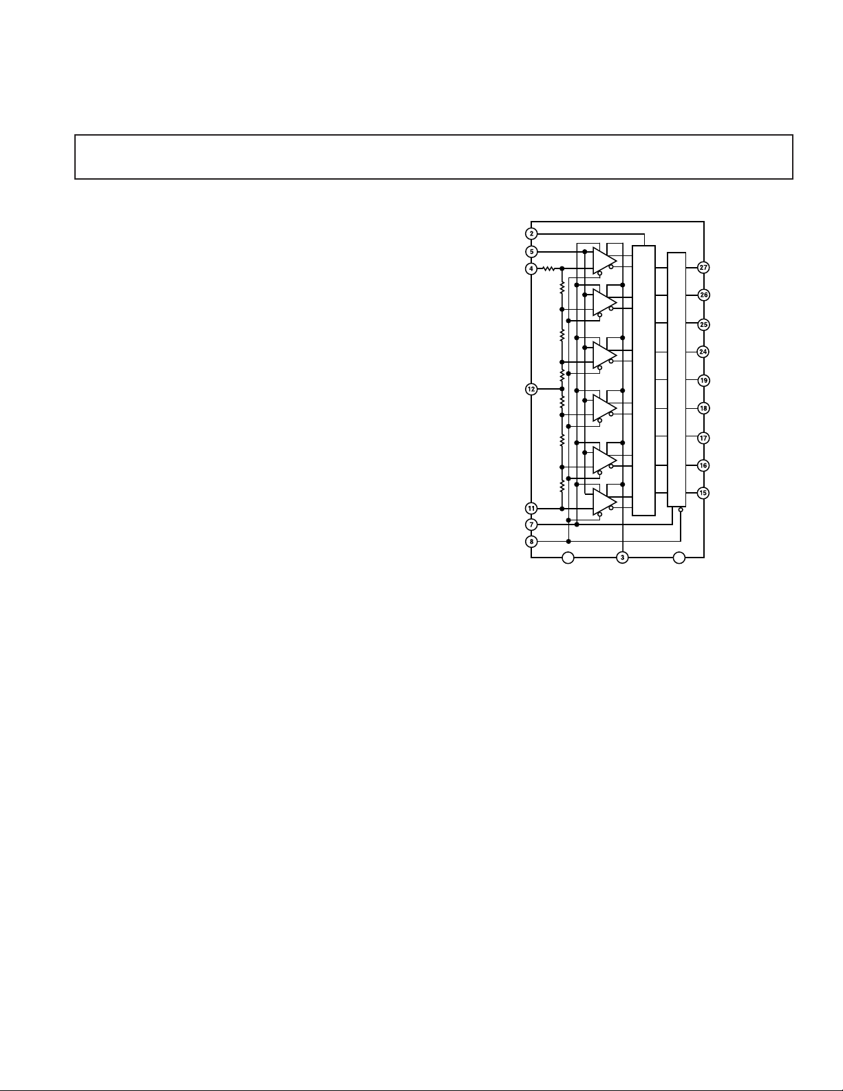
FUNCTIONAL BLOCK DIAGRAM
256
255
128
127
2
1
D
E
C
O
D
I
N
G
L
O
G
I
C
L
A
T
C
H
R
R
R
R/2
R/2
R
R
OVERFLOW
INHIBIT
ANALOG IN
+V
REF
REF
MID
–V
REF
ENCODE
ENCODE
GND HYSTERESIS
–V
S
BIT 2
BIT 3
BIT 4
BIT 5
BIT 6
BIT 7
BIT 8 (MSB)
OVERFLOW
AD9002
BIT 1 (LSB)
FEATURES
150 MSPS Encode Rate
Low Input Capacitance: 17 pF
Low Power: 750 mW
–5.2 V Single Supply
MIL-STD-883 Compliant Versions Available
APPLICATIONS
Radar Systems
Digital Oscilloscopes/ATE Equipment
Laser/Radar Warning Receivers
Digital Radio
Electronic Warfare (ECM, ECCM, ESM)
Communication/Signal Intelligence
GENERAL DESCRIPTION
The AD9002 is an 8-bit, high-speed, analog-to-digital converter.
The AD9002 is fabricated in an advanced bipolar process that
allows operation at sampling rates in excess of 150 megasamples/
second. Functionally, the AD9002 is comprised of 256 parallel
comparator stages whose outputs are decoded to drive the ECL
compatible output latches.
An exceptionally wide large signal analog input bandwidth of
160 MHz is due to an innovative comparator design and very
close attention to device layout considerations. The wide input
bandwidth of the AD9002 allows very accurate acquisition of
high speed pulse inputs, without an external track-and-hold.
The comparator output decoding scheme minimizes false codes,
which is critical to high speed linearity.
The AD9002 provides an external hysteresis control pin that
can be used to optimize comparator sensitivity to further improve
performance. Additionally, the AD9002’s low power dissipation
of 750 mW makes it usable over the full extended temperature
range. The AD9002 also incorporates an overflow bit to indicate
overrange inputs. This overflow output can be disabled with the
overflow inhibit pin.
The AD9002 is available in two grades, one with 0.5 LSB linearity
and one with 0.75 LSB linearity. Both versions are offered in an
industrial grade, –25°C to +85°C, packaged in a 28-lead DIP
and a 28-leaded JLCC. The military temperature range devices,
–55°C to +125°C, are available in ceramic DIP and LCC pack-
ages and comply with MIL-STD-883 Class B.

REV. 0
–2–
AD9002–SPECIFICATIONS
ELECTRICAL CHARACTERISTICS
AD9002AD/AJ AD9002BD/BJ AD9002SD/SE AD9002TD/TE
Parameter Temp Min Typ Max Min Typ Max Min Typ Max Min Typ Max Unit
RESOLUTION 8 8 8 8 Bits
DC ACCURACY
Differential Linearity 25°C 0.6 0.75 0.4 0.5 0.6 0.75 0.4 0.5 LSB
Full 1.0 0.75 1.0 0.75 LSB
Integral Linearity 25°C 0.6 1.0 0.4 0.5 0.6 1.0 0.4 0.5 LSB
Full 1.2 1.2 1.2 1.2 LSB
No Missing Codes Full GUARANTEED GUARANTEED GUARANTEED GUARANTEED
INITIAL OFFSET ERROR
Top of Reference Ladder 25°C 8 14 8 14 8 14 8 14 mV
Full 17 17 17 17 mV
Bottom of Reference Ladder 25°C 4 10 4 10 4 10 4 10 mV
Full 12 12 12 12 mV
Offset Drift Coefficient Full 20 20 20 20 µV/°C
ANALOG INPUT
Input Bias Current
1
25°C 60 200 60 200 60 200 60 200 µA
Full 200 200 200 200 µA
Input Resistance 25°C 25 200 25 200 25 200 25 200 kΩ
Input Capacitance 25°C 1722 1722 1722 1722 pF
Large Signal Bandwidth
2
25°C 160 160 160 160 MHz
Input Slew Rate
3
25°C 440 440 440 440 V/µs
REFERENCE INPUT
Reference Ladder Resistance 25°C 40 80 110 40 80 110 40 80 110 40 80 110 Ω
Ladder Temperature Coefficient 0.25 0.25 0.25 0.25 Ω/°C
Reference Input Bandwidth 25°C10101010MHz
DYNAMIC PERFORMANCE
Conversion Rate 25°C 125 150 125 150 125 150 125 150 MSPS
Aperture Delay 25°C 1.3 1.3 1.3 1.3 ns
Aperture Uncertainty (Jitter) 25°C15151515ps
Output Delay (t
PD
)
4, 5
25°C 2.5 3.7 5.5 2.5 3.7 5.5 2.5 3.7 5.5 2.5 3.7 5.5 ns
Transient Response
6
25°C6666ns
Overvoltage Recovery Time
7
25°C6666ns
Output Rise Time
4
25°C 3.0 3.0 3.0 3.0 ns
Output Fall Time
4
25°C 2.5 2.5 2.5 2.5 ns
Output Time Skew
4, 8
25°C 0.6 0.6 0.6 0.6 ns
ENCODE INPUT
Logic “1” Voltage
4
Full –1.1 –1.1 –1.1 –1.1 V
Logic “0” Voltage
4
Full –1.5 –1.5 –1.5 –1.5 V
Logic “1” Current Full 150 150 150 150 µA
Logic “0” Current Full 120 120 120 120 µA
Input Capacitance 25°C3333pF
Encode Pulsewidth (Low)
9
25°C 1.5 1.5 1.5 1.5 ns
Encode Pulsewidth (High)
9
25°C 1.5 1.5 1.5 1.5 ns
OVERFLOW INHIBIT INPUT
0 V Input Current Full 144 300 144 300 144 300 144 300 µA
AC LINEARITY
10
Effective Bits
11
25°C 7.6 7.6 7.6 7.6 Bits
In-Band Harmonics
dc to 1.23 MHz 25°C4855 4855 4855 4855 dB
dc to 9.3 MHz 25°C50505050dB
dc to 19.3 MHz 25°C44444444dB
Signal-to-Noise Ratio
12
25°C 46 47.6 46 47.6 46 47.6 46 47.6 dB
Two Tone Intermod Rejection
13
25°C60606060dB
DIGITAL OUTPUTS
4
Logic “1” Voltage Full –1.1 –1.1 –1.1 –1.1 V
Logic “0” Voltage Full –1.5 –1.5 –1.5 –1.5 V
POWER SUPPLY
14
Supply Current (–5.2 V) 25°C 145 175 145 175 145 175 145 175 mA
Full 200 200 200 200 mA
Nominal Power Dissipation 25°C 750 750 750 750 mW
Reference Ladder Dissipation 25°C50505050mW
Power Supply Rejection Ratio
15
25°C 0.8 1.5 0.8 1.5 0.8 1.5 0.8 1.5 mV/V
NOTES
1
Measured with AIN = 0 V.
2
Measured by FFT analysis where fundamental is –3 dBc.
3
Input slew rate derived from rise time (10 to 90%) of full scale input.
4
0utputs terminated through 100 Ω to –2 V.
5
Measured from ENCODE in to data out for LSB only.
6
For full-scale step input, 8-bit accuracy is attained in specified time.
7
Recovers to 8-bit accuracy in specified time after 150% full-scale input overvoltage.
8
Output time skew includes high-to-low and low-to-high transitions as well as
bit-to-bit time skew differences.
9
ENCODE signal rise/fall times should be less than 10 ns for normal operation.
10
Measured at 125 MSPS encode rate.
11
Analog input frequency = 1.23 MHz.
12
RMS signal to rms noise, with 1.23 MHz analog input signal.
13
Input signals 1 V p-p @ 1.23 MHz and 1 V p-p @ 2.30 MHz.
14
Supplies should remain stable within ± 5% for normal operation.
15
Measured at –5.2 V ± 5%.
Specifications subject to change without notice.
(–V
S
= –5.2 V; Differential Reference Voltage = 2.0 V; unless otherwise noted)

REV. F
AD9002
–3–
ABSOLUTE MAXIMUM RATINGS
1
Supply Voltage (–V
S
) . . . . . . . . . . . . . . . . . . . . . . . . . . . –6 V
Analog-to-Digital Supply Voltage Differential . . . . . . . . 0.5 V
Analog Input Voltage . . . . . . . . . . . . . . . . . . . . –V
S
to +0.5 V
Digital Input Voltage . . . . . . . . . . . . . . . . . . . . . . . –V
S
to 0 V
Reference Input Voltage (+V
REF
– V
REF
)
2
. . . –3.5 V to +0.1 V
Differential Reference Voltage . . . . . . . . . . . . . . . . . . . . 2.1 V
Reference Midpoint Current . . . . . . . . . . . . . . . . . . . . ±4 mA
ENCODE to ENCODE Differential Voltage . . . . . . . . . . . 4 V
Digital Output Current . . . . . . . . . . . . . . . . . . . . . . . . 20 mA
Operating Temperature Range
AD9002AD/BD/AJ/BJ . . . . . . . . . . . . . . . –25°C to +85°C
AD9002SE/SD/TD/TE . . . . . . . . . . . . . . –55°C to +125°C
Storage Temperature Range . . . . . . . . . . . . –65°C to +150°C
Junction Temperature
3
. . . . . . . . . . . . . . . . . . . . . . . . 150°C
Lead Soldering Temperature (10 sec) . . . . . . . . . . . . . 300°C
NOTES
1
Absolute maximum ratings are limiting values, to be applied individually, and
beyond which the serviceability of the circuit may be impaired. Functional
operability under any of these conditions is not necessarily implied. Exposure to
absolute maximum rating conditions for extended periods of time may affect device
reliability.
2
+V
REF
≥ –V
REF
under all circumstances.
3
Maximum junction temperature (t
J
max) should not exceed 175°C for ceramic
packages, and 150°C for plastic packages:
t
J
= PD (θ
JA
) + t
A
PD (θ
JC
) + t
C
where
PD = power dissipation
θ
JA
= thermal impedance from junction to ambient (°C/W)
θ
JC
= thermal impedance from junction to case (°C/W)
t
A
= ambient temperature (°C)
t
C
= case temperature (°C)
Typical thermal impedances are:
Ceramic DIP θ
JA
= 56°C/W; θ
JC
= 20°C/W
Ceramic LCC θ
JA
= 69°C/W; θ
JC
= 23°C/W
PLCC θ
JA
= 60°C/W; θ
JC
= 19°C/W.
Recommended Operating Conditions
Input Voltage
Parameter Min Nominal Max
–V
S
–5.46 –5.20 –4.94
+V
REF
–V
REF
0.0 V +0.1
–V
REF
–2.1 –2.0 +V
REF
Analog Input –V
REF
+V
REF
EXPLANATION OF TEST LEVELS
Test Level I – 100% production tested.
Test Level II – 100% production tested at 25°C, and sample
tested at specified temperatures.
Test Level III – Sample tested only.
Test Level IV – Parameter is guaranteed by design and
characterization testing.
Test Level V – Parameter is a typical value only.
Test Level VI –
All devices are 100% production tested at
25°C. 100% production tested at temperature
extremes for extended temperature devices;
sample tested at temperature extremes for
commercial/industrial devices.
ORDERING GUIDE
Package
Model Linearity Temperature Range Option*
AD9002AD 0.75 LSB –25°C to +85°C D-28
AD9002BD 0.50 LSB –25°C to +85°C D-28
AD9002AJ 0.75 LSB –25°C to +85°C J-28
AD9002BJ 0.50 LSB –25°C to +85°C J-28
AD9002SD/883B 0.75 LSB –55°C to +125°C D-28
AD9002SE/883B 0.75 LSB –55°C to +125°C E-28A
AD9002TD/883B 0.50 LSB –55°C to +125°C D-28
AD9002TE/883B 0.50 LSB –55°C to +125°C E-28A
*D = Ceramic DIP; E = Leadless Ceramic Chip Carrier; J = Ceramic Chip
Carrier, J-Formed Leads.
CAUTION
ESD (electrostatic discharge) sensitive device. Electrostatic charges as high as 4000 V readily
accumulate on the human body and test equipment and can discharge without detection.
Although the AD9002 features proprietary ESD protection circuitry, permanent damage may
occur on devices subjected to high-energy electrostatic discharges. Therefore, proper ESD
precautions are recommended to avoid performance degradation or loss of functionality.
WARNING!
ESD SENSITIVE DEVICE
 Loading...