


Analog Devices AD7804BN, AD7805CR, AD7805BST, AD7805BRS, AD7805BR Datasheet
...
a+3.3 V to +5 V Quad/Octal 10-Bit DACs
AD7804/AD7805/AD7808/AD7809*
FEATURES
Four 10-Bit DACs in One Package
Serial and Parallel Loading Facilities Available AD7804 Quad 10-Bit Serial Loading
AD7805 Quad 10-Bit Parallel Loading AD7808 Octal 10-Bit Serial Loading AD7809 Octal 10-Bit Parallel Loading
+3.3 V to +5 V Operation Power-Down Mode Power-On Reset
Standby Mode (All DACs/Individual DACs) Low Power All CMOS Construction
10-Bit Resolution
Double Buffered DAC Registers Dual External Reference Capability
APPLICATIONS
Optical Disk Drives
Instrumentation and Communication Systems
Process Control and Voltage Setpoint Control
Trim Potentiometer Replacement
Automatic Calibration
GENERAL DESCRIPTION
The AD7804/AD7808 are quad/octal 10-bit digital-to-analog converters, with serial load capabilities, while the AD7805/AD7809 are quad/octal 10-bit digital-to-analog converters with parallel load capabilities. These parts operate from a +3.3 V to +5 V
(±10%) power supply and incorporates an on-chip reference.
These DACs provide output signals in the form of VBIAS ± VSWING. VSWING is derived internally from VBIAS. On-chip control registers include a system control register and channel control registers.
The system control register has control over all DACs in the package. The channel control registers allow individual control of DACs. The complete transfer function of each individual
DAC can be shifted around the VBIAS point using an on-chip Sub DAC. All DACs contain double buffered data inputs,
which allow all analog outputs to be simultaneously updated using the asynchronous LDAC input.
Control Features |
Channels Controlled |
Main DAC |
Sub DAC |
Hardware Clear |
All |
Ï |
Ï |
System Control |
|
|
|
Power Down1 |
All |
Ï |
Ï |
System Standby2 |
All |
Ï |
Ï |
System Clear |
All |
Ï |
|
Input Coding |
All |
Ï |
Ï |
Channel Control |
|
|
|
Channel Standby2 |
Selective |
Ï |
Ï |
Channel Clear |
Selective |
Ï |
|
VBIAS |
Selective |
Ï |
Ï |
NOTES
1Power-down function powers down all internal circuitry including the reference. 2Standby functions power down all circuitry except for the reference.
REV. A
Information furnished by Analog Devices is believed to be accurate and reliable. However, no responsibility is assumed by Analog Devices for its use, nor for any infringements of patents or other rights of third parties which may result from its use. No license is granted by implication or otherwise under any patent or patent rights of Analog Devices.
FUNCTIONAL BLOCK DIAGRAMS
|
|
AVDD |
DVDD AGND DGND |
|
|
REFOUT |
1.23V REF |
POWER ON |
AD7804/ |
VOUTF* |
|
|
RESET |
|
|||
|
|
|
VOUTE* |
||
REFIN |
|
|
|
AD7808 |
|
|
|
|
|
|
|
|
AVDD |
|
VBIAS |
|
|
|
DIVIDER |
|
VOUTD |
||
COMP |
|
|
MUX |
DAC D |
|
|
CHANNEL D |
|
DATA |
DAC |
|
|
CONTROL REG |
|
REGISTER |
REGISTER |
|
|
|
|
VBIAS |
VOUTC |
|
|
|
|
MUX |
DAC C |
|
|
CHANNEL C |
|
DATA |
DAC |
|
|
CONTROL REG |
|
REGISTER |
REGISTER |
|
|
|
|
VBIAS |
VOUTB |
|
|
|
|
MUX |
DAC B |
|
|
CHANNEL B |
|
DATA |
DAC |
|
|
CONTROL REG |
|
REGISTER |
REGISTER |
|
|
|
|
VBIAS |
VOUTA |
|
|
|
|
MUX |
DAC A |
|
PD** |
CHANNEL A |
|
DATA |
DAC |
|
|
CONTROL REG |
|
REGISTER |
REGISTER |
|
|
SYSTEM |
|
|
|
VOUTH* |
|
CONTROL REG |
|
|
|
|
FSIN |
INPUT SHIFT |
|
VOUTG* |
||
CLKIN |
REGISTER & |
|
|
||
SDIN |
CONTROL LOGIC |
|
|
||
|
|
|
|
|
|
|
ONLY AD7804 SHOWN FOR CLARITY |
CLR LDAC |
|
||
*SHOWS ADDITIONAL CHANNELS ON THE AD7808 **PIN ON THE AD7808 ONLY
|
|
|
AVDD DVDD |
AGND DGND |
|
||
REFOUT |
|
1.23V REF |
POWER ON |
AD7805/ |
VOUTF* |
||
|
|
|
RESET |
|
VOUTE* |
||
REFIN |
|
|
|
|
|
AD7809 |
|
|
|
|
|
|
|
||
|
|
|
|
|
|
|
|
|
|
AVDD |
|
|
VBIAS |
|
|
|
|
DIVIDER |
|
|
VOUTD |
||
COMP |
|
|
|
MUX |
DAC D |
||
|
|
CHANNEL D |
|
DATA |
DAC |
|
|
|
CONTROL REG |
|
REGISTER |
REGISTER |
|
||
|
|
|
|
|
VBIAS |
VOUTC |
|
|
|
|
|
MUX |
DAC C |
||
|
|
CHANNEL C |
|
DATA |
DAC |
|
|
|
CONTROL REG |
|
REGISTER |
REGISTER |
|
||
|
|
|
|
|
VBIAS |
VOUTB |
|
|
|
|
|
MUX |
DAC B |
||
|
|
CHANNEL B |
|
DATA |
DAC |
|
|
|
CONTROL REG |
|
REGISTER |
REGISTER |
|
||
|
|
|
|
|
VBIAS |
VOUTA |
|
|
|
|
|
MUX |
DAC A |
||
|
|
CHANNEL A |
|
DATA |
DAC |
|
|
PD** |
CONTROL REG |
|
REGISTER |
REGISTER |
|
||
|
|
|
|
|
|
|
|
|
SYSTEM |
|
|
|
|
|
|
|
CONTROL REG |
|
|
|
|
VOUTH* |
|
CS |
CONTROL |
INPUT |
|
|
|
VOUTG* |
|
WR |
LOGIC |
REGISTER |
|
|
|||
|
MODE A0 |
A1 A2** |
DB9 DB2 |
DB1 DB0 |
CLR LDAC |
|
|
ONLY AD7805 SHOWN FOR CLARITY
*SHOWS ADDITIONAL CHANNELS ON THE AD7809 **PIN ON THE AD7809 ONLY
*Patent pending. Index on Page 26.
One Technology Way, P.O. Box 9106, Norwood, MA 02062-9106, U.S.A.
Tel: 781/329-4700 |
World Wide Web Site: http://www.analog.com |
Fax: 781/326-8703 |
© Analog Devices, Inc., 1998 |
AD7804/AD7805/AD7808/AD7809
AD7804/AD7805–SPECIFICATIONS (AVDD and DVDD = 3.3 V 6 10% to 5 V 6 10%; AGND = DGND = 0 V; Reference = Internal Reference; CL = 100 pF; RL = 2 kV to GND. Sub DAC at Midscale. All specifications TMIN to TMAX unless otherwise noted.)
Parameter |
|
B Grade1 |
|
C Grade1 |
Units |
Comments |
||
STATIC PERFORMANCE |
|
|
|
|
|
|
|
|
MAIN DAC |
|
|
|
|
|
|
|
|
Resolution |
10 |
|
10 |
|
Bits |
|
||
Relative Accuracy |
±3 |
|
±3 |
|
LSB max |
|
||
Gain Error |
±3 |
|
±3 |
|
% FSR max |
|
||
Bias Offset Error2 |
|
–80/+40 |
|
|
–80/+40 |
|
mV max |
DAC Code = 0.5 Full Scale |
Zero-Scale Error3 |
|
–VBIAS |
/ +40 |
|
–VBIAS |
/ +40 |
mV max |
DAC Code = 000H for Offset Binary |
|
16 |
16 |
|
|
||||
|
|
|
|
|
||||
Monotonicity |
9 |
|
10 |
|
Bits |
and 200H for Twos Complement Coding |
||
Minimum Load Resistance |
2 |
|
2 |
|
kΩ min |
|
||
SUB DAC |
|
|
|
|
|
|
|
|
Resolution |
8 |
|
8 |
|
Bits |
|
||
Differential Nonlinearity |
±0.125 |
|
±0.125 |
|
LSB typ |
Refers to an LSB of the Main DAC |
||
|
±0.5 |
|
±0.5 |
|
LSB max |
|
||
|
|
|
|
|
|
|
|
|
OUTPUT CHARACTERISTICS |
|
VBIAS ± 15/16 × VBIAS |
|
VBIAS ± 15/16 × VBIAS |
|
|
||
Output Voltage Range3 |
|
|
V |
Twos Complement Coding |
||||
|
|
VBIAS/16 to 31/16 × VBIAS |
|
VBIAS/16 to 31/16 × VBIAS |
V |
Offset Binary Coding |
||
Voltage Output Settling Time to 10 Bits |
4 |
|
4 |
|
µs max |
Typically 1.5 µs |
||
Slew Rate |
2.5 |
|
2.5 |
|
V/µs typ |
|
||
Digital-to-Analog Glitch Impulse |
1 |
|
1 |
|
nV-s typ |
1 LSB Change Around the Major Carry |
||
Digital Feedthrough |
0.5 |
|
0.5 |
|
nV-s typ |
|
||
Digital Crosstalk |
0.5 |
|
0.5 |
|
nV-s typ |
|
||
Analog Crosstalk |
±0.2 |
|
±0.2 |
|
LSB typ |
|
||
DC Output Impedance |
2 |
|
2 |
|
Ω typ |
VDD ± 10% |
||
Power Supply Rejection Ratio |
0.002 |
|
0.002 |
|
%/% typ |
|||
DAC REFERENCE INPUTS |
|
|
|
|
|
|
|
|
REF IN Range |
|
1.0 to VDD/2 |
|
1.0 to VDD/2 |
V min to V max |
|
||
REF IN Input Leakage |
±1 |
|
±1 |
|
µA max |
Typically ±1 nA |
||
DIGITAL INPUTS |
|
|
|
|
|
|
|
|
Input High Voltage, VIH @ VDD = 5 V |
2.4 |
|
2.4 |
|
V min |
|
||
Input High Voltage, VIH @ VDD = 3.3 V |
2.1 |
|
2.1 |
|
V min |
|
||
Input Low Voltage, VIL @ VDD = 5 V |
0.8 |
|
0.8 |
|
V max |
|
||
Input Low Voltage, VIL @ VDD = 3.3 V |
0.6 |
|
0.6 |
|
V max |
|
||
Input Leakage Current |
±10 |
|
|
µA max |
|
|
|
|
Input Capacitance |
10 |
|
10 |
|
pF max |
|
||
Input Coding |
|
Twos Comp/Binary |
|
Twos Comp/Binary |
|
|
||
REFERENCE OUTPUT |
|
|
|
|
|
|
|
|
REF OUT Output Voltage |
1.23 |
|
1.23 |
|
V nom |
|
||
REF OUT Error |
±8 |
|
±8 |
|
% max |
|
||
REF OUT Temperature Coefficient |
|
–100 |
|
|
–100 |
|
ppm/°C typ |
|
REF OUT Output Impedance |
5 |
|
5 |
|
kΩ nom |
|
||
POWER REQUIREMENTS |
|
|
|
|
|
|
|
|
VDD (AVDD and DVDD) |
3/5.5 |
|
3/5.5 |
|
V min to V max |
|
||
IDD (AIDD Plus DIDD) |
|
|
|
|
|
|
|
Excluding Load Currents |
Normal Mode |
12 |
|
12 |
|
mA max |
VIH = VDD, VIL = DGND |
||
System Standby (SSTBY) Mode |
250 |
|
250 |
|
µA |
VIH = VDD, VIL = DGND |
||
Power-Down (PD) Mode |
|
|
|
|
|
|
|
|
@ +25°C |
0.8 |
|
0.8 |
|
µA max |
VIH = VDD, VIL = DGND |
||
TMIN–TMAX |
1.5 |
|
1.5 |
|
µA max |
|
||
Power Dissipation |
|
|
|
|
|
|
|
Excluding Power Dissipated in Load |
Normal Mode |
66 |
|
66 |
|
mW max |
|
||
System Standby (SSTBY) Mode |
1.38 |
|
1.38 |
|
mW max |
|
||
Power-Down (PD) Mode |
|
|
|
|
|
|
|
|
@ +25°C |
4.4 |
|
4.4 |
|
µW max |
|
||
TMIN–TMAX |
8.25 |
|
8.25 |
|
µW max |
|
||
NOTES
1Temperature range is – 40°C to +85°C. 2Can be minimized using the Sub DAC.
3VBIAS is the center of the output voltage swing and can be VDD/2, Internal Reference or REFIN as determined by MX1 and MX0 in the channel control register. Specifications subject to change without notice.
–2– |
REV. A |
AD7804/AD7805/AD7808/AD7809
AD7808/AD7809–SPECIFICATIONS (AVDD and DVDD = 3.3 V 6 10% to 5 V 6 10%; AGND = DGND = 0 V; Reference = Internal Reference; CL = 100 pF; RL = 2 kV to GND. Sub DAC at Midscale. All specifications TMIN to TMAX unless otherwise noted.)
Parameter |
B Grade1 |
Units |
Comments |
STATIC PERFORMANCE |
|
|
|
MAIN DAC |
|
|
|
Resolution |
10 |
Bits |
|
Relative Accuracy |
±4 |
LSB max |
|
Gain Error |
±3 |
% FSR max |
|
Bias Offset Error2 |
±60 |
mV max |
DAC Code = 0.5 Full Scale |
Zero-Scale Error |
±35 |
mV max |
DAC Code = 000H for Offset Binary |
Monotonicity |
9 |
Bits |
and 200H for Twos Complement |
Minimum Load Resistance |
2 |
kΩ min |
Coding |
SUB DAC |
|
|
|
Resolution |
8 |
Bits |
|
Differential Nonlinearity |
±0.125 |
LSB typ |
Refers to an LSB of the Main DAC |
|
±0.5 |
LSB max |
|
OUTPUT CHARACTERISTICS |
VBIAS ± 15/16 × VBIAS |
|
|
Output Voltage Range3 |
V |
Twos Complement Coding |
|
|
VBIAS/16 to 31/16 × VBIAS |
V |
Offset Binary Coding |
Voltage Output Settling Time to 10 Bits |
4 |
µs max |
Typically 1.5 µs |
Slew Rate |
2.5 |
V/µs typ |
|
Digital-to-Analog Glitch Impulse |
1 |
nV-s typ |
1 LSB Change Around the Major Carry |
Digital Feedthrough |
0.5 |
nV-s typ |
|
Digital Crosstalk |
0.5 |
nV-s typ |
|
Analog Crosstalk |
±0.2 |
LSB typ |
|
DC Output Impedance |
2 |
Ω typ |
VDD ± 10% |
Power Supply Rejection Ratio |
0.002 |
%/% typ |
|
DAC REFERENCE INPUTS |
|
|
|
REF IN Range |
1.0 to VDD/2 |
V min to V max |
|
REF IN Input Leakage |
±1 |
µA max |
Typically ±1 nA |
DIGITAL INPUTS |
|
|
|
Input High Voltage, VIH @ VDD = 5 V |
2.4 |
V min |
|
Input High Voltage, VIH @ VDD = 3.3 V |
2.1 |
V min |
|
Input Low Voltage, VIL @ VDD = 5 V |
0.8 |
V max |
|
Input Low Voltage, VIL @ VDD = 3.3 V |
0.6 |
V max |
|
Input Leakage Current |
±10 |
µA max |
|
Input Capacitance |
8 |
pF max |
|
Input Coding |
Twos Comp/Binary |
|
|
REFERENCE OUTPUT |
|
|
|
REF OUT Output Voltage |
1.23 |
V nom |
|
REF OUT Error |
±8 |
% max |
|
REF OUT Temperature Coefficient |
–100 |
ppm/°C typ |
|
REF OUT Output Impedance |
5 |
kΩ nom |
|
POWER REQUIREMENTS |
|
|
|
VDD (AVDD and DVDD) |
3/5.5 |
V min to V max |
|
IDD (AIDD Plus DIDD) |
|
|
Excluding Load Currents |
Normal Mode |
18 |
mA max |
VIH = VDD, VIL = DGND |
System Standby (SSTBY) Mode |
250 |
µA max |
VIH = VDD, VIL = DGND |
Power-Down (PD) Mode |
|
|
|
@ +25°C |
1 |
µA max |
VIH = VDD, VIL = DGND |
TMIN–TMAX |
3 |
µA max |
|
Power Dissipation |
|
|
Excluding Power Dissipated in Load |
Normal Mode |
99 |
mW max |
|
System Standby (SSTBY) Mode |
1.38 |
mW max |
|
Power-Down (PD) Mode |
|
|
|
@ +25°C |
5.5 |
µW max |
|
TMIN–TMAX |
16.5 |
µW max |
|
NOTES
1Temperature range is – 40°C to +85°C. 2Can be minimized using the Sub DAC.
3VBIAS is the center of the output voltage swing and can be VDD/2, Internal Reference or REFIN as determined by MX1 and MX0 in the channel control register. Specifications subject to change without notice.
REV. A |
–3– |
AD7804/AD7805/AD7808/AD7809
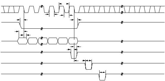
AD7804/AD7808 TIMING CHARACTERISTICS1(VDD = 3.3 V 6 10% to 5 V 6 10%; AGND = DGND = 0 V; Reference =
Internal Reference. All specifications TMIN to TMAX unless otherwise noted.)
|
Limit at TMIN, TMAX |
|
|
Parameter |
All Versions |
Units |
Description |
|
|
|
|
t1 |
100 |
ns min |
CLKIN Cycle Time |
t2 |
40 |
ns min |
CLKIN High Time |
t3 |
40 |
ns min |
CLKIN Low Time |
t4 |
30 |
ns min |
FSIN Setup Time |
t5 |
30 |
ns min |
Data Setup Time |
t6 |
5 |
ns min |
Data Hold Time |
t6A |
6 |
ns min |
LDAC Hold Time |
t7 |
90 |
ns max |
FSIN Hold Time |
|
20 |
ns min |
LDAC, CLR Pulsewidth |
t8 |
40 |
ns min |
|
t9 |
100 |
ns min |
LDAC Setup Time |
NOTES
1Sample tested during initial release and after any redesign or process change that may affect this parameter. All input signals are specified with tr = tf = 5 ns and timed from a voltage of (VIL + VIH)/2.
Specifications subject to change without notice.
|
|
|
t1 |
CLKIN(I) |
|
|
|
|
|
t2 |
t3 |
|
|
|
|
|
t4 |
|
t7 |
FSIN(I) |
|
|
|
|
t5 |
t6 |
|
|
|
|
|
SDIN(I) |
DB15 |
|
DB0 |
|
|
|
t6A |
|
|
|
t5 |
LDAC1 |
|
|
|
LDAC2 |
|
|
t9 |
|
|
t8 |
|
CLR |
|
|
t8 |
1TIMING REQUIREMENTS FOR SYNCHRONOUS LDAC UPDATE OR LDAC MAY BE TIED PERMANENTLY LOW IF REQUIRED.
2TIMING REQUIREMENTS FOR ASYNCHRONOUS LDAC UPDATE.
Figure 1. Timing Diagram for AD7804 and AD7808
–4– |
REV. A |
AD7804/AD7805/AD7808/AD7809
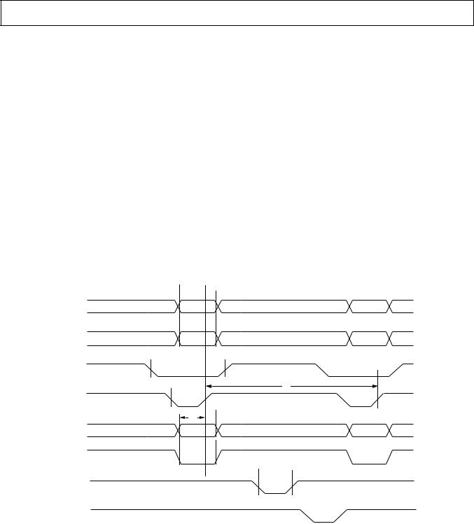
AD7805/AD7809 TIMING CHARACTERISTICS1 (VDD = 3.3 V 6 10% to 5 V 6 10%; AGND = DGND = 0 V; Reference
= Internal Reference. All specifications TMIN to TMAX unless otherwise noted.)
|
Limit at TMIN, TMAX |
|
|
Parameter |
All Versions |
Unit |
Description |
|
|
|
|
t1 |
25 |
ns min |
Mode Valid to Write Setup Time |
t2 |
4.5 |
ns min |
Mode Valid to Write Hold Time |
t3 |
25 |
ns min |
Address Valid to Write Setup Time |
t4 |
4.5 |
ns min |
Address Valid to Write Hold Time |
t5 |
25 |
ns min |
Data Setup Time |
t6 |
4.5 |
ns min |
Data Hold Time |
t6A |
6 |
ns min |
LDAC Valid to Write Hold Time |
t7 |
40 |
ns min |
Chip Select to Write Setup Time |
t8 |
0 |
ns min |
Chip Select to Write Hold Time |
t9 |
40 |
ns min |
Write Pulsewidth |
t10 |
100 |
ns min |
Time Between Successive Writes |
t11 |
40 |
ns min |
LDAC, CLR Pulsewidth |
t12 |
100 |
ns min |
Write to LDAC Setup Time |
NOTE
1Sample tested during initial release and after any redesign or process change that may affect this parameter. All input signals are specified with tr = tf = 5 ns and timed from a voltage of (VIL + VIH)/2.
Specifications subject to change without notice.
 t1
t1 
 t2
t2 
MODE
 t4
t4 
 t3
t3 
A0, A1, A2
t8  t7
t7 


CS
t10
 t9
t9 
WR
 t6
t6 
t5
DATA
 t6A
t6A
LDAC 1
 t12
t12
 t11
t11
LDAC 2
 t11
t11

CLR
1TIMING REQUIREMENTS FOR SYNCHRONOUS LDAC UPDATE OR LDAC MAY BE TIED PERMANENTLY LOW IF REQUIRED.
2TIMING REQUIREMENTS FOR ASYNCHRONOUS LDAC UPDATE.
Figure 2. Timing Diagram for AD7805/AD7809 Parallel Write
REV. A |
–5– |

AD7804/AD7805/AD7808/AD7809
ABSOLUTE MAXIMUM RATINGS1
(TA = +25°C unless otherwise noted)
DVDD to DGND . . . . . . . . . . . . |
. . . . . . . . . . |
. . –0.3 V to +7 V |
AVDD to AGND . . . . . . . . . . . . |
. . . . . . . . . . |
. . –0.3 V to +7 V |
AGND to DGND . . . . . . . . . . . |
. . . . . . . . . . |
. . –0.3 V + 0.3 V |
Digital Input Voltage to DGND |
. . . . . –0.3 V to DVDD + 0.3 V |
|
Analog Input Voltage to AGND |
. . . . . –0.3 V to AVDD + 0.3 V |
|
COMP to AGND . . . . . . . . . . . |
. . . . –0.3 V to AVDD + 0.3 V |
|
REF OUT to AGND . . . . . . . . . . |
. . . . . . . . |
–0.3 V to + AVDD |
REF IN to AGND . . . . . . . . . . . . |
. . . –0.3 V to AVDD + 0.3 V |
|
VOUT to AGND2 . . . . . . . . . . . . . |
. . . –0.3 V to AVDD + 0.3 V |
|
Input Current to Any Pin Except Supplies3 . |
. . . . . . . ± 10 mA |
|
Operating Temperature Range |
|
|
AD7804/AD7805 Commercial Plastic |
–40°C to +85°C |
|
(B, C Versions) . . . . . . . . . . . |
. . . . . . . . . |
|
AD7808/AD7809 Commercial Plastic |
–40°C to +85°C |
|
(B, C Versions) . . . . . . . . . . . |
. . . . . . . . . |
|
Storage Temperature Range . . . . |
. . . . . . . . |
–65°C to +150°C |
Junction Temperature . . . . . . . . . |
. . . . . . . . . |
. . . . . . . +150°C |
SOIC (R-16) Package, Power Dissipation . . . |
. . . . . . 450 mW |
|
θJA Thermal Impedance . . . . . . |
. . . . . . . . . |
. . . . . . . 75°C/W |
Lead Temperature, Soldering |
|
+215°C |
Vapor Phase (60 sec) . . . . . . |
. . . . . . . . . |
|
Infrared (15 sec) . . . . . . . . . . |
. . . . . . . . . |
. . . . . . . +220°C |
PDIP (N-16) Package, Power Dissipation . . . |
. . . . . . 670 mW |
|
θJA Thermal Impedance . . . . . . |
. . . . . . . . . |
. . . . . . 116°C/W |
Lead Temperature, Soldering (10 sec) . . . . |
. . . . . . . +260°C |
|
SOIC (R-24) Package, Power Dissipation . . . |
. . . . . . 450 mW |
|
θJA Thermal Impedance . . . . . . |
. . . . . . . . . |
. . . . . . . 75°C/W |
Lead Temperature, Soldering |
|
+215°C |
Vapor Phase (60 sec) . . . . . . |
. . . . . . . . . |
|
Infrared (15 sec) . . . . . . . . . . |
. . . . . . . . . |
. . . . . . . +220°C |
PDIP (N-24) Package, Power Dissipation . . . . . . . . . 670 mW
θJA Thermal Impedance . . . . . . . . . . . . . . . . . . . . . 105°C/W Lead Temperature, Soldering (10 sec) . . . . . . . . . . . +260°C
SOIC (R-28) Package, Power Dissipation . . . . . . . . . 875 mW
θJA Thermal Impedance . . . . . . . . . . . . . . . . . . . . . . 70°C/W Lead Temperature, Soldering
Vapor Phase (60 sec) . . . . . . . . . . . . . . . . . . . . . . +215°C Infrared (15 sec) . . . . . . . . . . . . . . . . . . . . . . . . . . +220°C PDIP (N-28) Package, Power Dissipation . . . . . . . . . 875 mW
θJA Thermal Impedance . . . . . . . . . . . . . . . . . . . . . . 75°C/W Lead Temperature, Soldering (10 sec) . . . . . . . . . . . +260°C
SSOP (RS-28) Package, Power Dissipation . . . . . . . . 875 mW
θJA Thermal Impedance . . . . . . . . . . . . . . . . . . . . . 110°C/W Lead Temperature, Soldering
Vapor Phase (60 sec) . . . . . . . . . . . . . . . . . . . . . . +215°C Infrared (15 sec) . . . . . . . . . . . . . . . . . . . . . . . . . . +220°C TQFP (ST-44B) Package, Power Dissipation . . . . . . 450 mW
θJA Thermal Impedance . . . . . . . . . . . . . . . . . . . . . 116°C/W Lead Temperature, Soldering
Vapor Phase (60 sec) . . . . . . . . . . . . . . . . . . . . . . +215°C Infrared (15 sec) . . . . . . . . . . . . . . . . . . . . . . . . . . +220°C
NOTES
1Stresses above those listed under Absolute Maximum Ratings may cause permanent damage to the device. This is a stress rating only; functional operation of the device at these or any other conditions above those listed in the operational sections of this specification is not implied. Exposure to absolute maximum rating conditions for extended periods may affect device reliability.
2The outputs may be shorted to voltages in this range provided the power dissipation of the package is not exceeded.
3Transient currents of up to 100 mA will not cause SCR latch-up.
ORDERING GUIDE
|
Supply |
Temperature |
Relative |
|
Package |
Model |
Voltage |
Range |
Accuracy |
Package Descriptions |
Options |
AD7804BN |
3.3 V to 5 V |
–40°C to +85°C |
± 3 LSB |
16-Lead Plastic DIP |
N-16 |
AD7804BR |
3.3 V to 5 V |
–40°C to +85°C |
± 3 LSB |
16-Lead Small Outline IC |
R-16 |
AD7805BN |
3.3 V to 5 V |
–40°C to +85°C |
± 3 LSB |
28-Lead Plastic DIP |
N-28 |
AD7805BR |
3.3 V to 5 V |
–40°C to +85°C |
± 3 LSB |
28 Lead Small Outline IC |
R-28 |
AD7805BRS |
3.3 V to 5 V |
–40°C to +85°C |
± 3 LSB |
28-Lead Shrink Small Outline Package |
RS-28 |
AD7805CR |
3.3 V to 5 V |
–40°C to +85°C |
± 3 LSB |
28-Lead Small Outline IC |
R-28 |
AD7808BN |
3.3 V to 5 V |
–40°C to +85°C |
± 4 LSB |
24-Lead Plastic DIP |
N-24 |
AD7808BR |
3.3 V to 5 V |
–40°C to +85°C |
± 4 LSB |
24 Lead Small Outline IC |
R-24 |
AD7809BST |
3.3 V to 5 V |
–40°C to +85°C |
± 4 LSB |
44-Lead Thin Plastic Quad Flatpack (TQFP) |
ST-44B |
CAUTION
ESD (electrostatic discharge) sensitive device. Electrostatic charges as high as 4000 V readily accumulate on the human body and test equipment and can discharge without detection. Although these devices feature proprietary ESD protection circuitry, permanent damage may occur on devices subjected to high energy electrostatic discharges. Therefore, proper ESD precautions are recommended to avoid performance degradation or loss of functionality.
WARNING! |
ESD SENSITIVE DEVICE |
–6– |
REV. A |

|
|
|
|
AD7804/AD7805/AD7808/AD7809 |
|
|
|
|
|
|
|
|
AD7804/AD7808 PIN FUNCTION DESCRIPTION |
|
|
|
|
|
|
AD7804 |
AD7808 |
|
|
|
Pin No. |
Pin No. |
Mnemonic |
|
Description |
|
|
|
|
|
1 |
1, 6 |
AGND |
|
Ground reference point for analog circuitry. |
2, 3 |
2, 3 |
VOUTB, VOUTA |
|
Analog output voltage from the DACs. |
4 |
4 |
REFOUT |
|
Reference Output. This is a bandgap reference and is typically 1.23 V. |
|
5 |
PD |
|
Active low input used to put the part into low power mode reducing current consumption |
|
|
|
|
to 1 A. |
|
7, 8 |
VOUTF, VOUTE |
|
Analog output voltages from the DACs. |
5 |
9 |
FSIN |
|
Level-triggered control input (active low). This is the frame synchronization signal for the |
|
|
|
|
input data. When FSIN goes low, it enables the input shift register and data is transferred |
|
|
|
|
on the falling edges of CLKIN. |
6 |
10 |
LDAC |
|
LDAC Input. When this digital input is taken low, all DAC registers are simultaneously |
|
|
|
|
updated with the contents of the data registers. If LDAC is tied permanently low, or is |
|
|
|
|
low on the sixteenth falling clock edge with timing similar to that of SDIN, an automatic |
|
|
|
|
update will take place. |
7 |
11 |
SDIN |
|
Serial Data Input. These devices accept a 16-bit word. Data is clocked into the input shift |
|
|
|
|
register on the falling edge of CLKIN. |
8 |
12 |
DGND |
|
Ground reference point for digital circuitry. |
9 |
13 |
DVDD |
|
Digital Power Supply. |
10 |
14 |
CLKIN |
|
Clock Input. Data is clocked into the input shift register on the falling edges of CLKIN. |
|
|
|
|
Duty Cycle should be between 40% and 60%. |
11 |
15 |
CLR |
|
Asynchronous CLR Input. When this input is taken low, all Main DAC outputs are |
|
|
|
|
cleared either to VBIAS or to VBIAS/16 volts. All Sub DACs are also cleared and thus the |
|
|
|
|
transfer function of the Main DAC will remain centered around the VBIAS point. |
|
16 |
NC |
|
No Connect. This pin should be left open circuit. |
|
17, 18 |
VOUTH, VOUTG |
|
Analog output voltages from the DACs. |
12 |
20 |
REFIN |
|
This is an external reference input for the DACs. When this reference is selected for a |
|
|
|
|
DAC in the control register, the analog output from the selected DAC swings around this |
|
|
|
|
point. |
13 |
21 |
COMP |
|
Compensation Pin. This pin provides an output from the internal VDD/2 divider and is |
|
|
|
|
provided for ac bypass purposes only. This pin should be decoupled with 1 nF capacitors |
|
|
|
|
to both AVDD and AGND. This pin can be overdriven with an external reference, thus |
|
|
|
|
giving the facility for two external references on the part. |
14, 15 |
22, 23 |
VOUTD, VOUTC |
|
Analog output voltage from the DACs. |
16 |
19, 24 |
AVDD |
|
Analog Power Supply. +3.3 V to +5 V. |
AD7804 PIN CONFIGURATION |
AD7808 PIN CONFIGURATION |
|||||||||||||
|
|
|
|
|
|
|
AGND |
|
|
|
|
|
AVDD |
|
AGND |
1 |
|
|
|
16 |
AVDD |
1 |
|
|
|
24 |
|||
|
|
|
|
|
|
|
|
|
VOUT C |
|||||
VOUT B |
|
|
|
|
|
VOUT C |
VOUT B |
2 |
|
|
|
23 |
||
2 |
|
|
|
15 |
VOUT A |
|
|
|
|
|
VOUT D |
|||
|
|
|
3 |
|
|
|
22 |
|||||||
VOUT A |
|
|
|
|
|
VOUT D |
|
|
|
|||||
3 |
AD7804 |
14 |
REFOUT |
4 |
|
|
|
21 |
COMP |
|||||
REFOUT |
|
|
COMP |
|
|
|
||||||||
4 |
13 |
PD |
5 |
|
|
|
20 |
REFIN |
||||||
|
|
TOP VIEW |
|
REFIN |
AD7808 |
|||||||||
FSIN |
5 |
(Not to Scale) |
12 |
AGND |
6 |
TOP VIEW |
19 |
AVDD |
||||||
LDAC |
|
|
|
|
|
CLR |
||||||||
6 |
|
|
|
11 |
V F |
7 |
(Not to Scale) |
18 |
V |
G |
||||
SDIN |
|
|
|
|
|
CLKIN |
OUT |
|
|
|
|
|
OUT |
|
7 |
|
|
|
10 |
VOUT E |
8 |
|
|
|
17 |
VOUT H |
|||
DGND |
|
|
|
|
|
DVDD |
|
|
|
|||||
|
|
|
|
|
|
|
|
|
|
|
|
|
||
8 |
|
|
|
9 |
FSIN |
9 |
|
|
|
16 |
NC |
|
||
|
|
|
|
|
|
|
LDAC |
|
|
|
|
|
CLR |
|
|
|
|
|
|
|
|
10 |
|
|
|
15 |
|
||
|
|
|
|
|
|
|
|
|||||||
|
|
|
|
|
|
|
SDIN |
|
|
|
|
|
CLKIN |
|
|
|
|
|
|
|
|
11 |
|
|
|
14 |
|||
|
|
|
|
|
|
|
DGND |
|
|
|
|
|
DVDD |
|
|
|
|
|
|
|
|
12 |
|
|
|
13 |
|||
|
|
|
|
|
|
|
|
|
|
|
|
|
|
|
|
|
|
|
|
|
|
|
NC = NO CONNECT |
|
|
||||
REV. A |
–7– |

AD7804/AD7805/AD7808/AD7809
|
|
AD7805/AD7809 PIN FUNCTION DESCRIPTIONS |
|
AD7805 |
AD7809 |
|
|
Pin No. |
Pin No. |
Mnemonic |
Description |
|
1, 11, 13, |
NC |
No Connect. These pins should be left open circuit. |
|
20, 33 |
|
|
1 |
2, 5, 39, 40 |
AGND |
Ground reference point for analog circuitry. |
2, 3 |
41, 42 |
VOUTB, VOUTA |
Analog output voltages from the DACs. |
4 |
43 |
REFOUT |
Reference Output. This is a bandgap reference and is typically 1.23 V. |
5–10, |
3, 4, 6, 7, 9, |
DB9–DB2 |
Data Inputs. DB9 to DB2 are the 8 MSBs of the data word. |
12, 13 |
10, 15, 23 |
|
|
19, 20 |
24, 26 |
DB1, DB0 |
DB1 and DB0 function as the 2 LSBs of the 10-bit word in 10-bit parallel mode but |
|
|
|
have other functions when BYTE loading structure is used. |
|
8, 12 |
VOUTF, VOUTE |
Analog output voltages from the DACs. |
11 |
14 |
LDAC |
LDAC Input. When this digital input is taken low, all DAC registers are simultaneously |
|
|
|
updated with the contents of the DAC data registers. If LDAC is permanently tied low, or is |
|
|
|
low during the rising edge of WR similar to data inputs, an automatic update will take place. |
14 |
16 |
DGND |
Ground reference point for digital circuitry. |
15 |
17 |
DVDD |
Digital Power Supply. |
16 |
18 |
WR |
Write Input WR is an active low logic input which is used in conjunction with CS and |
|
|
|
the address pins to write data to the relevant registers. |
17 |
21 |
CS |
Chip Select. Active low logic input. |
18 |
19 |
CLR |
Asynchronous CLR Input. When this input is taken low, all Main DAC outputs are |
|
|
|
cleared either to VBIAS or to VBIAS/16 volts. All Sub DACs are also cleared and thus the |
|
22, 25 |
VOUTH, VOUTG |
transfer function of the MAIN DAC will remain centered around the VBIAS point. |
|
Analog output voltages from the DACs. |
||
21, 22 |
27, 29, 30 |
A2, A1, A0 |
DAC Address Inputs. These digital inputs are used in conjunction with CS and WR to |
|
|
|
determine which DAC channel control register or DAC data register is loaded from the |
|
|
|
input register. These address bits are don’t cares when writing to the system control register. |
23 |
31 |
MODE |
Logic Input. Logic high enables writing to the DAC data registers, a logic low enables |
|
|
|
writing to the control registers. |
24 |
32 |
REFIN |
This is an external reference input for the DAC. When this reference is selected for the DAC |
|
|
|
in the control register, the analog output from the selected DAC swings around this point. |
25 |
34 |
COMP |
Compensation Pin. This pin provides an output from the internal VDD/2 divider and is |
|
|
|
provided for ac bypass purposes only. This pin should be decoupled with 1 nF capacitors |
|
|
|
to both AVDD and AGND. This pin can be overdriven with an external reference, thus |
|
|
|
giving the facility for two external references on the part. |
26, 27 |
35, 36 |
VOUTD, VOUTC |
Analog output voltages from the DACs. |
28 |
28, 37, 38 |
AVDD |
Analog Power Supply. |
|
44 |
PD |
Active low input used to put the part into low power mode reducing current consump- |
|
|
|
tion to 1 A. |
AD7805 PIN CONFIGURATION
AGND |
|
|
|
|
|
AVDD |
1 |
|
|
|
28 |
||
VOUT B |
|
|
|
|
|
VOUT C |
2 |
|
|
|
27 |
||
VOUT A |
|
|
|
|
|
VOUT D |
3 |
|
|
|
26 |
||
REFOUT |
|
|
|
|
|
COMP |
4 |
|
|
|
25 |
||
DB9 |
|
|
|
|
|
REFIN |
5 |
|
|
|
24 |
||
DB8 |
|
|
|
|
|
MODE |
6 |
AD7805 |
23 |
||||
DB7 |
|
|
A0 |
|||
7 |
TOP VIEW |
22 |
||||
DB6 |
|
(Not to Scale) |
|
A1 |
||
8 |
21 |
|||||
DB5 |
|
|
|
|
|
DB0 |
9 |
|
|
|
20 |
||
|
|
|
|
|
|
DB1 |
DB4 |
10 |
|
|
|
19 |
|
|
|
|
|
|
|
CLR |
LDAC |
11 |
|
|
|
18 |
|
|
|
|
|
|
|
|
DB3 |
12 |
|
|
|
17 |
CS |
|
|
|
|
|
|
|
DB2 |
13 |
|
|
|
16 |
WR |
|
|
|
|
|
|
|
DGND |
14 |
|
|
|
15 |
DVDD |
|
|
|
|
|
|
|
AD7809 PIN CONFIGURATION
|
|
PD |
REFOUT |
V |
V |
AGND |
AGND |
AV |
AV |
V |
V |
COMP |
|
|
|
|
|
A |
B |
|
|
DD |
DD |
C |
D |
|
|
|
|
|
|
OUT |
OUT |
|
|
OUT |
OUT |
|
|
||
|
|
44 |
43 |
42 |
41 |
40 |
39 |
38 |
37 |
36 |
35 |
34 |
|
NC |
1 |
PIN 1 |
|
|
|
|
|
|
|
|
33 |
NC |
|
AGND |
2 |
|
|
|
|
|
|
|
|
32 |
REFIN |
||
IDENTIFIER |
|
|
|
|
|
|
|||||||
DB9 |
3 |
|
|
|
|
|
|
|
|
|
|
31 |
MODE |
DB8 |
4 |
|
|
|
|
|
|
|
|
|
|
30 |
A0 |
AGND |
5 |
|
|
|
|
AD7809 |
|
|
|
29 |
A1 |
||
DB7 |
6 |
|
|
|
|
|
|
|
28 |
AVDD |
|||
|
|
|
TOP VIEW |
|
|
|
|||||||
DB6 |
7 |
|
|
|
(Not to Scale) |
|
|
27 |
A2 |
||||
VOUTF |
8 |
|
|
|
|
|
|
|
|
|
|
26 |
DB0 |
DB5 |
9 |
|
|
|
|
|
|
|
|
|
|
25 |
VOUTG |
DB4 10 |
|
|
|
|
|
|
|
|
|
|
24 |
DB1 |
|
NC 11 |
|
|
|
|
|
|
|
|
|
|
23 |
DB2 |
|
|
|
12 |
13 |
14 |
15 |
16 |
17 |
18 |
19 |
20 |
21 |
22 |
|
|
|
V |
NC |
LDAC |
DB3 |
DGND |
DV |
WR |
CLR |
NC |
CS |
V |
|
NC = NO CONNECT |
E |
|
|
|
|
DD |
|
|
|
|
H |
|
|
OUT |
|
|
|
|
|
|
|
|
OUT |
|
|||
|
|
|
|
|
|
|
|
|
|
|
|||
–8– |
REV. A |
AD7804/AD7805/AD7808/AD7809
TERMINOLOGY
Relative Accuracy
For the DACs, relative accuracy or endpoint nonlinearity is a measure of the maximum deviation, in LSBs, from a straight line passing through the endpoints of the DAC transfer function. Figures 32 and 33 show the linearity at 3 V and 5 V respectively.
Differential Nonlinearity
Differential nonlinearity is the difference between the measured change and the ideal 1 LSB change between any two adjacent codes. A specified differential nonlinearity of ±1 LSB maximum ensures monotonicity.
Bias Offset Error
If the DACs are ideal, the output voltage of any DAC with
midscale code loaded will be equal to VBIAS where VBIAS is selected by MX1 and MX0 in the control register. The DAC bias
offset error is the difference between the actual output voltage and VBIAS, expressed in mV.
Gain Error
The difference between the actual and ideal analog output range, expressed as a percent of full-scale range. It is the deviation in slope of the DAC transfer characteristic from ideal.
Zero-Scale Error
The zero-scale error is the actual output minus the ideal output from any DAC when zero code is loaded to the DAC. If offset binary coding is used, the code loaded is 000Hex, and if twos complement coding is used, a code of 200HEX is loaded to the DAC to calculate the zero-scale error. Zero-scale error is expressed in mV.
Digital-to-Analog Glitch Impulse
Digital-to-analog glitch impulse is the impulse injected into the
analog output when the digital inputs change state with the DAC selected and the LDAC used to update the DAC. It is
normally specified as the area of the glitch in nV-s and is measured when the digital input code is changed by 1 LSB at the major carry transition. Regardless of whether offset binary or twos complement coding is used, the major carry transition occurs at
the analog output voltage change of VBIAS to VBIAS – 1 LSB or vice versa.
Digital Feedthrough
Digital feedthrough is a measure of the impulse injected into the analog output of a DAC from the digital inputs of the same DAC but is measured when the DAC is not updated. It is specified in nV secs and is measured with a full-scale code change on the data bus, i.e., from all 0s to all 1s and vice versa.
Digital Crosstalk
Digital crosstalk is the glitch impulse transferred to the output of one converter due to a digital code change to another DAC. It is specified in nV-s.
Analog Crosstalk
Analog crosstalk is a change in output of any DAC in response to a change in the output of one or more of the other DACs. It is measured in LSBs.
Power Supply Rejection Ratio (PSRR)
This specification indicates how the output of the DAC is affected by changes in the power supply voltage. Power-supply rejection ratio is quoted in terms of % change in output per % change in VDD for full-scale output of the DAC. VDD is varied
±10%.
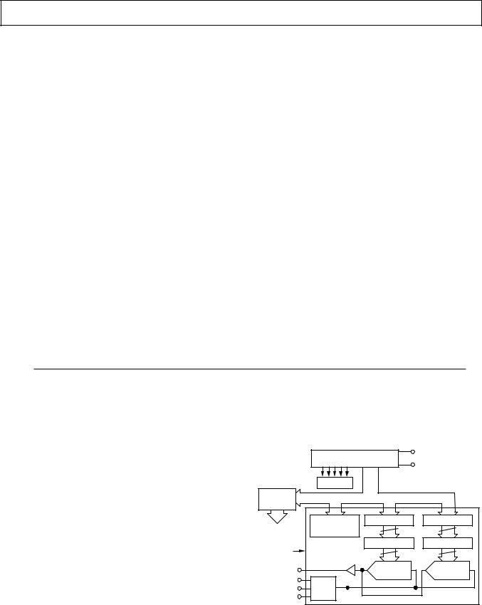
AD7804/AD7808 INTERFACE SECTION
The AD7804 and AD7808 are serial input devices. Three lines control the serial interface, FSIN, CLKIN and SDIN. The timing diagram is shown in Figure 1.
Two mode bits (MD1 and MD0) which are DB13 and DB14 of the serial word written to the AD7804/AD7808 are used to determine whether writing is to the DAC data registers or the control registers of the device. These parts contain a system control register for controlling the operation of all DACs in the package as well as a channel control register for controlling the operation of each individual DAC. Table I shows how to access these registers.
Table I. Register Selection Table for the AD7804/AD7808
MD1 |
MD0 |
Function |
|
|
|
0 |
0 |
Write enable to system control register. |
0 |
1 |
Write enable to channel control register. |
1 |
X |
Write enable to DAC data registers. |
|
|
|
When the FSIN input goes low, data appearing on the SDIN line is clocked into the input register on each falling edge of CLKIN. Data to be transferred to the AD7804/AD7808 is loaded MSB first. Figure 4 shows the loading sequence for the AD7804/AD7808 system control register, Figure 5 shows the
sequence for the channel control register write, and Figures 6 and 7 show the sequence for loading data to the Main and Sub DAC data registers. Figure 3 shows the internal registers associated with the AD7804/AD7808 serial interface DACs. Only one DAC structure is shown for clarity.
16-BIT
FSIN
INPUT SHIFT REGISTER

 CLKIN
CLKIN
SDIN
|
DECODER |
|
|
SYSTEM |
|
|
|
CONTROL |
|
|
|
REGISTER |
|
|
|
|
CHANNEL |
DATA REGISTER |
DATA REGISTER |
TO ALL |
CONTROL |
|
|
CHANNELS |
REGISTER |
10 |
8 |
SINGLE |
|
DAC REGISTER |
DAC REGISTER |
|
|
|
|
CHANNEL |
|
10 |
8 |
|
|
||
VOUT |
|
10-BIT DAC |
8-BIT DAC |
|
(MAIN DAC) |
(SUB DAC) |
|
INTERNAL VREF |
VBIAS |
|
|
VDD/2 |
MUX |
|
|
REFIN |
|
|
|
Figure 3. AD7804/AD7808 Internal Registers
REV. A |
–9– |
 Loading...