


 Loading...
Analog Devices AD73322LYST, AD73322LYRU, AD73322LYR, AD73322LAST, AD73322LARU Datasheet
...a Low Cost, Low Power CMOS
General-Purpose Dual Analog Front End
AD73322L
FEATURES
Two 16-Bit A/D Converters
Two 16-Bit D/A Converters
Programmable Input/Output Sample Rates 78 dB ADC SNR
78 dB DAC SNR
64 kS/s Maximum Sample Rate –90 dB Crosstalk
Low Group Delay (25 s Typ per ADC Channel, 50 s Typ per DAC Channel)
Programmable Input/Output Gain
Flexible Serial Port which Allows Up to Four Dual Codecs to be Connected in Cascade Giving Eight I/O Channels
Single (2.7 V to 3.3 V) Supply Operation 50 mW Typ Power Consumption at 3.0 V Temperature Range: –40 C to +105 C
On-Chip Reference
28-Lead SOIC, TSSOP, and 44-Lead LQFP Packages
APPLICATIONS
General-Purpose Analog I/O
Speech Processing
Cordless and Personal Communications
Telephony
Active Control of Sound and Vibration
Data Communications
Wireless Local Loop
FUNCTIONAL BLOCK DIAGRAM
|
AVDD1 AVDD2 |
DVDD |
|
|
|
AD73322L |
|
VFBP1 |
|
|
|
VINP1 |
ADC CHANNEL 1 |
|
SDI |
VINN1 |
|
||
|
|
|
|
VFBN1 |
|
|
SDIFS |
VOUTP1 |
DAC CHANNEL 1 |
|
SCLK |
VOUTN1 |
|
||
|
|
|
|
REFOUT |
|
SPORT |
SE |
REFERENCE |
|
RESET |
|
REFCAP |
|
||
|
|
|
|
VFBP2 |
|
|
|
VINP2 |
ADC CHANNEL 2 |
|
MCLK |
VINN2 |
|
|
|
|
|
|
|
VFBN2 |
|
|
|
VOUTP2 |
DAC CHANNEL 2 |
|
SDOFS |
VOUTN2 |
|
SDO |
|
|
|
||
|
|
|
|
|
AGND1 AGND2 |
DGND |
|
GENERAL DESCRIPTION
The AD73322L is a dual front-end processor for general purpose applications including speech and telephony. It features two 16-bit A/D conversion channels and two 16-bit D/A conversion channels. Each channel provides 78 dB signal-to-noise ratio over a voiceband signal bandwidth. It also features an input-to-output gain network in both the analog and digital domains. This is featured on both codecs and can be used for impedance matching or scaling when interfacing to Subscriber Line Interface Circuits (SLICs).
The AD73322L is particularly suitable for a variety of applications in the speech and telephony area, including low bit rate, high quality compression, speech enhancement, recognition and synthesis. The low group delay characteristic of the part makes it suitable for single or multichannel active control applications.
REV. 0
Information furnished by Analog Devices is believed to be accurate and reliable. However, no responsibility is assumed by Analog Devices for its use, nor for any infringements of patents or other rights of third parties that may result from its use. No license is granted by implication or otherwise under any patent or patent rights of Analog Devices.
The A/D and D/A conversion channels feature programmable input/output gains with ranges 38 dB and 21 dB respectively. An on-chip reference voltage is included to allow singlesupply operation.
The sampling rate of the codecs is programmable with four separate settings offering 64 kHz, 32 kHz, 16 kHz, and 8 kHz sampling rates (from a master clock of 16.384 MHz).
A serial port (SPORT) allows easy interfacing of single or cascaded devices to industry standard DSP engines. The SPORT transfer rate is programmable to allow interfacing to both fast and slow DSP engines.
The AD73322L is available in 28-lead SOIC, 28-lead TSSOP, and 44-lead LQFP packages.
One Technology Way, P.O. Box 9106, Norwood, MA 02062-9106, U.S.A.
Tel: 781/329-4700 |
www.analog.com |
Fax: 781/326-8703 |
© Analog Devices, Inc., 2001 |
AD73322L–SPECIFICATIONS1 |
(AVDD = 3 V 10%; DVDD = 3 V 10%; DGND = AGND = 0 V, fDMCLK = |
||||
16.384 MHz, fSAMP = 8 kHz; TA = TMIN to TMAX, unless otherwise noted.) |
|||||
|
A, Y Versions |
|
|
||
Parameter |
Min |
Typ |
Max |
Unit |
Test Conditions/Comments |
|
|
|
|
|
|
REFERENCE |
|
|
|
|
|
REFCAP |
|
|
|
|
|
Absolute Voltage, VREFCAP |
1.08 |
1.2 |
1.32 |
V |
|
REFCAP TC |
|
50 |
|
ppm/°C |
0.1 µF Capacitor Required from |
REFOUT |
|
|
|
Ω |
REFCAP to AGND2 |
Typical Output Impedance |
|
130 |
|
|
|
Absolute Voltage, VREFOUT |
1.08 |
1.2 |
1.32 |
V |
Unloaded |
Minimum Load Resistance |
|
1 |
|
kΩ |
|
Maximum Load Capacitance |
|
100 |
|
pF |
|
|
|
|
|
|
|
INPUT AMPLIFIER |
|
±1.0 |
|
|
|
Offset |
|
|
mV |
Max Output Swing = (1.578/1.2) × VREFCAP |
|
Maximum Output Swing |
|
1.578 |
|
V |
|
Feedback Resistance |
|
50 |
|
kΩ |
fC = 32 kHz |
Feedback Capacitance |
|
100 |
|
pF |
|
ANALOG GAIN TAP |
|
|
|
|
|
Gain at Maximum Setting |
|
+1 |
|
|
|
Gain at Minimum Setting |
|
–1 |
|
|
|
Gain Resolution |
|
5 |
|
Bits |
Gain Step Size = 0.0625 |
Gain Accuracy |
|
±1.0 |
|
% |
Output Unloaded |
Settling Time |
|
1.0 |
|
µs |
Tap Gain Change of –FS to +FS |
Delay |
|
0.5 |
|
µs |
|
ADC SPECIFICATIONS |
|
|
|
|
DAC Unloaded |
Maximum Input Range at VIN2, 3 |
|
1.578 |
|
V p-p |
Measured Differentially |
|
|
–2.85 |
|
dBm |
Max Input = (1.578/1.2) × VREFCAP |
Nominal Reference Level at VIN |
|
1.0954 |
|
V p-p |
Measured Differentially |
(0 dBm0) |
|
–6.02 |
|
dBm |
|
Absolute Gain |
|
|
|
|
|
PGA = 0 dB |
–2.0 |
–0.7 |
+0.5 |
dB |
1.0 kHz, 0 dBm0 |
Gain Tracking Error |
|
±0.1 |
|
dB |
1.0 kHz, +3 dBm0 to –50 dBm0 |
Signal to (Noise + Distortion) |
|
|
|
|
Refer to TPC 1. |
PGA = 0 dB |
70 |
78 |
|
dB |
300 Hz to 3400 Hz; fSAMP = 8 kHz, PUIA = 0 |
|
|
79 |
|
dB |
300 Hz to 3400 Hz; fSAMP = 8 kHz, PUIA = 1 |
Total Harmonic Distortion |
|
77.5 |
|
dB |
0 Hz to fSAMP/2; fSAMP = 8 kHz |
|
|
|
|
|
|
PGA = 0 dB |
|
–86 |
–75 |
dB |
300 Hz to 3400 Hz; fSAMP = 8 kHz |
Intermodulation Distortion |
|
–61 |
|
dB |
PGA = 0 dB |
Idle Channel Noise Crosstalk |
|
–72 |
|
dBm0 |
PGA = 0 dB |
ADC-to-DAC |
|
–107 |
|
dB |
ADC Input Signal Level: 1.0 kHz, 0 dBm0 |
|
|
|
|
|
DAC Input at Idle |
ADC-to-ADC |
|
–92 |
|
dB |
ADC1 Input Signal Level: 1.0 kHz, 0 dBm0 |
|
|
|
|
|
ADC2 Input at Idle. Input Amplifiers Bypassed |
|
|
–93 |
|
dB |
Input Amplifiers Included in Input Channel |
DC Offset |
–20 |
0 |
+20 |
mV |
PGA = 0 dB |
Power Supply Rejection |
|
–65 |
|
dB |
Input Signal Level at AVDD and DVDD |
Group Delay4, 5 |
|
|
|
µs |
Pins: 1.0 kHz, 100 mV p-p Sine Wave |
|
25 |
|
|
||
Input Resistance at PGA2, 4, 6 |
|
20 |
|
kΩ |
Input Amplifiers Bypassed |
DIGITAL GAIN TAP |
|
|
|
|
|
Gain at Maximum Setting |
|
+1 |
|
|
|
Gain at Minimum Setting |
|
–1 |
|
|
|
Gain Resolution |
|
16 |
|
Bits |
Tested to 5 MSBs of Settings |
Delay |
|
25 |
|
µs |
Includes DAC Delay |
Settling Time |
|
100 |
|
µs |
Tap Gain Change from –FS to +FS; Includes |
|
|
|
|
|
DAC Settling Time |
–2– |
REV. 0 |
AD73322L
|
|
A, Y Versions |
|
|
|
Parameter |
Min |
Typ |
Max |
Unit |
Test Conditions/Comments |
|
|
|
|
|
|
DAC SPECIFICATIONS |
|
|
|
|
DAC Unloaded |
Maximum Voltage Output Swing2 |
|
|
|
|
|
Single-Ended |
|
1.578 |
|
V p-p |
PGA = 6 dB |
|
|
–2.85 |
|
dBm |
Max Output = (1.578/1.2) × VREFCAP |
Differential |
|
3.156 |
|
V p-p |
PGA = 6 dB |
Nominal Voltage Output Swing (0 dBm0) |
|
3.17 |
|
dBm |
Max Output = 2 × ([1.578/1.2] × VREFCAP) |
|
|
|
|
|
|
Single-Ended |
|
1.0954 |
|
V p-p |
PGA = 6 dB |
|
|
–6.02 |
|
dBm |
|
Differential |
|
2.1909 |
|
V p-p |
PGA = 6 dB |
|
|
0 |
|
dBm |
|
Output Bias Voltage |
|
1.2 |
|
V |
REFOUT Unloaded |
Absolute Gain |
–1.75 |
–0.6 |
+0.75 |
dB |
1.0 kHz, 0 dBm0; Unloaded |
Gain Tracking Error |
|
± 0.1 |
|
dB |
1.0 kHz, +3 dBm0 to –50 dBm0 |
Signal to (Noise + Distortion) at 0 dBm0 |
|
|
|
|
Refer to TPC 2. |
PGA = 0 dB |
72 |
78.5 |
|
dB |
300 Hz to 3400 Hz; fSAMP = 8 kHz |
Total Harmonic Distortion at 0 dBm0 |
|
|
|
|
|
PGA = 0 dB |
|
–89 |
–75 |
dB |
300 Hz to 3400 Hz; fSAMP = 8 kHz |
Intermodulation Distortion |
|
–77 |
|
dB |
PGA = 0 dB |
Idle Channel Noise Crosstalk |
|
–81 |
|
dBm0 |
PGA = 0 dB |
DAC-to-ADC |
|
–73 |
|
dB |
ADC Input Signal Level: AGND; DAC |
|
|
|
|
|
Output Signal Level: 1.0 kHz, 0 dBm0 |
|
|
|
|
|
Input Amplifiers Bypassed |
|
|
–74 |
|
dB |
Input Amplifiers Included in Input Channel |
DAC-to-DAC |
|
–102 |
|
dB |
DAC1 Output Signal Level: AGND; DAC2 |
|
|
|
|
|
Output Signal Level: 1.0 kHz, 0 dBm0 |
Power Supply Rejection |
|
–65 |
|
dB |
Input Signal Level at AVDD and DVDD |
Group Delay4, 5 |
|
|
|
µs |
Pins: 1.0 kHz, 100 mV p-p Sine Wave |
|
25 |
|
Interpolator Bypassed |
||
Output DC Offset2, 7 |
|
50 |
|
µs |
|
–50 |
+5 |
+60 |
mV |
|
|
Minimum Load Resistance, RL2, 8 |
|
|
|
Ω |
|
Single-Ended4 |
|
150 |
|
|
|
Differential |
|
150 |
|
Ω |
|
Maximum Load Capacitance, CL2, 8 |
|
|
|
|
|
Single-Ended |
|
500 |
|
pF |
|
Differential |
|
100 |
|
pF |
|
FREQUENCY RESPONSE |
|
|
|
|
|
(ADC and DAC)9 Typical Output |
|
|
|
|
|
Frequency (Normalized to FS) |
|
|
|
|
|
0 |
|
0 |
|
dB |
|
0.03125 |
|
–0.1 |
|
dB |
|
0.0625 |
|
–0.25 |
|
dB |
|
0.125 |
|
–0.6 |
|
dB |
|
0.1875 |
|
–1.4 |
|
dB |
|
0.25 |
|
–2.8 |
|
dB |
|
0.3125 |
|
–4.5 |
|
dB |
|
0.375 |
|
–7.0 |
|
dB |
|
0.4375 |
|
–9.5 |
|
dB |
|
> 0.5 |
|
< –12.5 |
|
dB |
|
REV. 0 |
–3– |
AD73322L
|
A, Y Versions |
|
|
|
|
Parameter |
Min |
Typ |
Max |
Unit |
Test Conditions/Comments |
|
|
|
|
|
|
LOGIC INPUTS |
|
|
|
|
|
VINH, Input High Voltage |
DVDD – 0.8 |
|
DVDD |
V |
|
VINL, Input Low Voltage |
0 |
|
0.8 |
V |
|
IIH, Input Current |
–10 |
|
+10 |
A |
|
CIN, Input Capacitance |
|
|
10 |
pF |
|
LOGIC OUTPUT |
|
|
|
|
|IOUT| ≤ 100 A |
VOH, Output High Voltage |
DVDD – 0.4 |
|
DVDD |
V |
|
VOL, Output Low Voltage |
0 |
|
0.4 |
V |
|IOUT| ≤ 100 A |
Three-State Leakage Current |
–10 |
|
+10 |
A |
|
POWER SUPPLIES |
|
|
|
|
|
AVDD1, AVDD2 |
2.7 |
|
3.3 |
V |
|
DVDD |
2.7 |
|
3.3 |
V |
|
10 |
|
|
|
|
See Table I |
IDD |
|
|
|
|
|
NOTES
1 Operating temperature range as follows: A Grade, TMIN = –40°C, TMAX = +85°C; Y Grade, TMIN = –40°C, TMAX = +105°C.
2 Test conditions: Input PGA set for 0 dB gain, Output PGA set for 6 dB gain, no load on analog outputs (unless otherwise noted). 3 At input to sigma-delta modulator of ADC.
4 Guaranteed by design.
5 Overall group delay will be affected by the sample rate and the external digital filtering.
6 The ADC’s input impedance is inversely proportional to DMCLK and is approximated by: (3.3 × 10¹¹)/DMCLK. 7 Between VOUTP1 and VOUTN1 or between VOUTP2 and VOUTN2.
8 At VOUT output.
9Frequency responses of ADC and DAC measured with input at audio reference level (the input level that produces an output level of –10 dBm0), with 38 dB preamplifier bypassed and input gain of 0 dB.
10 Test Conditions: no load on digital inputs, analog inputs ac-coupled to ground, no load on analog outputs.
Specifications subject to change without notice.
Table I. Current Summary (AVDD = DVDD = 3.3 V)
|
Analog |
Digital |
Total Current |
Total Current |
|
MCLK |
|
Conditions |
Current |
Current |
(Typ) |
(Max) |
SE |
ON |
Comments |
|
|
|
|
|
|
|
|
ADCs On Only |
3.4 |
6.3 |
9.7 |
12 |
1 |
YES |
REFOUT Disabled |
DACs On Only |
8.8 |
6.5 |
15.3 |
20 |
1 |
YES |
REFOUT Disabled |
ADCs and DACs On |
11.6 |
7.0 |
18.6 |
23 |
1 |
YES |
REFOUT Disabled |
ADCs and DACs |
|
|
|
|
|
|
|
and Input Amps On |
13.8 |
7.0 |
20.8 |
26 |
1 |
YES |
REFOUT Disabled |
ADCs and DACs |
|
|
|
|
|
|
|
and AGT On |
13.2 |
7.0 |
20.2 |
26 |
1 |
YES |
REFOUT Disabled |
All Sections On |
17.2 |
7.0 |
24.2 |
31 |
1 |
YES |
|
REFCAP On Only |
0.65 |
0 |
0.67 |
1.25 |
0 |
NO |
REFOUT Disabled |
REFCAP and |
|
|
|
|
|
|
|
REFOUT On Only |
2.56 |
0 |
2.57 |
4.5 |
0 |
NO |
|
All Sections Off |
0 |
1.25 |
1.25 |
1.8 |
0 |
YES |
MCLK Active Levels Equal to |
|
0 A |
12.5 A |
12.7 A |
40 A |
|
|
0 V and DVDD |
All Sections Off |
0 |
NO |
Digital Inputs Static and Equal |
||||
|
|
|
|
|
|
|
to 0 V or DVDD |
|
|
|
|
|
|
|
|
The above values are in mA and are typical values unless otherwise noted.
–4– |
REV. 0 |

AD73322L
Table II. Signal Ranges
|
|
|
|
|
3 V Power Supply |
|
|
|
|
|
5VEN = 0 |
|
|
|
|
|
|
VREFCAP |
|
|
|
|
1.2 V ± 10% |
VREFOUT |
|
|
|
|
1.2 V ± 10% |
ADC |
|
Maximum Input Range at VIN |
1.578 V p-p |
||
|
|
Nominal Reference Level |
|
1.0954 V p-p |
|
DAC |
|
Maximum Voltage Output Swing |
|
||
|
|
Single-Ended |
|
1.578 V p-p |
|
|
|
Differential |
|
3.156 V p-p |
|
|
|
Nominal Voltage Output Swing |
|
||
|
|
Single-Ended |
|
1.0954 V p-p |
|
|
|
Differential |
|
2.1909 V p-p |
|
|
|
Output Bias Voltage |
|
VREFOUT |
|
|
|
|
|
|
|
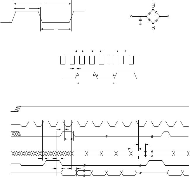
TIMING CHARACTERISTICS |
(AVDD = 3 V 10%; DVDD = 3 V 10%; AGND = DGND = 0 V; TA = TMlN to TMAX, unless |
||||
otherwise noted.) |
|
|
|||
|
|
|
|
|
|
|
Limit at |
|
|
|
|
Parameter |
TA = –40 C to +105 C |
|
Unit |
Description |
|
Clock Signals |
|
|
|
|
See Figure 1 |
t1 |
61 |
|
|
ns min |
MCLK Period |
t2 |
24.4 |
|
|
ns min |
MCLK Width High |
t3 |
24.4 |
|
|
ns min |
MCLK Width Low |
Serial Port |
|
|
|
|
See Figures 3 and 4 |
t4 |
t1 |
|
|
ns min |
SCLK Period |
t5 |
0.4 × t1 |
|
|
ns min |
SCLK Width High |
t6 |
0.4 × t1 |
|
|
ns min |
SCLK Width Low |
t7 |
20 |
|
|
ns min |
SDI/SDIFS Setup Before SCLK Low |
t8 |
0 |
|
|
ns min |
SDI/SDIFS Hold After SCLK Low |
t9 |
10 |
|
|
ns max |
SDOFS Delay from SCLK High |
t10 |
10 |
|
|
ns min |
SDOFS Hold After SCLK High |
t11 |
10 |
|
|
ns min |
SDO Hold After SCLK High |
t12 |
10 |
|
|
ns max |
SDO Delay from SCLK High |
t13 |
30 |
|
|
ns max |
SCLK Delay from MCLK |
Specifications subject to change without notice.
REV. 0 |
–5– |
AD73322L
t1 |
100 A |
IOL |
|
t2
TO OUTPUT |
2.1V |
|
PIN |
||
CL |
||
|
15pF |
t3 |
100 A IOH |
Figure 1. MCLK Timing |
|
|
|
|
|
|
|
|
|
|
|
|
Figure 2. Load Circuit for Timing Specifications |
|||||||||||
|
|
|
|
|
|
|
|
|
|
|
|
|
|
|
|
|
|
|
||||||
|
|
|
|
|
|
|
|
|
|
|
|
|
|
|
|
|
|
|
|
|
|
t3 |
|
|
|
|
|
|
|
|
|
|
|
|
|
|
|
|
|
|
|
|
|
|
|
|
|
||
|
|
|
|
|
|
t1 |
|
|
|
|
|
|
t2 |
|
|
|
|
|
|
|||||
|
||||||||||||||||||||||||
|
|
|
|
|
|
|
|
|
|
|
|
|
|
|
|
|
|
|
|
|
|
|
|
|
MCLK |
|
|
|
|
|
|
|
|
|
|
|
|
|
|
|
|
|
|
||||||
|
|
|
|
|
|
|
|
|
|
|
|
|
|
|
|
|
|
|
|
|
|
|
|
|
|
t13 |
|
|
|
|
|
|
|
|
|
|
|
|
|
|
|
|
|
|
|
|
|
|
|
|
|
|
|
|
|
|
|
|
|
|
|
|
|
|
|
|
|
|
|
|
|
|
|
|
|
|
|
|
|
|
|
|
|
|
|
|
|
|
|
|
|
|
|
|
|
|
|||
SCLK* |
|
|
|
|
|
|
t5 |
|
|
|
|
|
|
|
|
t6 |
|
|
|
|
|
|||
|
|
|
|
|
|
|
|
|
|
|
|
|
|
|
|
|
||||||||
|
|
|
|
|
|
|
|
|
|
|
|
|
|
|
|
|
|
|
|
|
|
|
|
|
|
|
|
|
|
|
|
|
|
|
|
|
|
|
|
|
|
|
|
|
|
||||
|
|
|
|
|
|
|
|
|
|
|
|
t4 |
|
|
|
|
|
|
|
|
||||
|
|
|
|
|
|
|
|
|
|
|
|
|
|
|
|
|
|
|
|
|||||
*SCLK IS INDIVIDUALLY PROGRAMMABLE IN FREQUENCY (MCLK/4 SHOWN HERE).
Figure 3. SCLK Timing
SE (I) |
|
|
|
|
|
|
|
|
|
SCLK (O) |
THREE- |
|
|
|
|
|
|
|
|
STATE |
|
|
|
|
|
|
|
|
|
|
|
|
|
t7 |
|
|
|
|
|
SDIFS (I) |
|
|
|
|
|
|
|
|
|
|
|
|
|
t8 |
|
|
|
|
|
|
|
|
|
|
|
|
|
t8 |
|
|
|
|
|
|
|
|
t7 |
|
|
SDI (I) |
|
|
|
D15 |
D14 |
D1 |
D0 |
|
D15 |
SDOFS (O) |
THREE- |
t9 |
|
t10 |
|
|
|
|
|
STATE |
|
|
|
|
|
|
|
|
|
|
THREE- |
|
t12 |
t11 |
|
|
|
|
|
SDO (O) |
STATE |
|
|
D15 |
D2 |
D1 |
D0 |
D15 |
D14 |
Figure 4. Serial Port (SPORT)
–6– |
REV. 0 |
AD73322L
ABSOLUTE MAXIMUM RATINGS*
(TA = 25°C unless otherwise noted)
AVDD, DVDD to GND . . . . . . . . . . . . . . . –0.3 V to +4.6 V AGND to DGND . . . . . . . . . . . . . . . . . . . . –0.3 V to +0.3 V Digital I/O Voltage to DGND . . . –0.3 V to (DVDD + 0.3 V) Analog I/O Voltage to AGND . . . –0.3 V to (AVDD + 0.3 V) Operating Temperature Range
Industrial (A Version) . . . . . . . . . . . . . . . –40°C to +85°C Extended (Y Version) . . . . . . . . . . . . . . . . –40°C to +105°C Storage Temperature Range . . . . . . . . . . . . –65°C to +150°C Maximum Junction Temperature . . . . . . . . . . . . . . . . 150°C SOIC, θJA Thermal Impedance . . . . . . . . . . . . . . . 71.4°C/W
Lead Temperature, Soldering
Vapor Phase (60 sec) . . . . . . . . . . . . . . . . . . . . . . . . 215°C Infrared (15 sec) . . . . . . . . . . . . . . . . . . . . . . . . . . . . 220°C LQFP, θJA Thermal Impedance . . . . . . . . . . . . . . . 53.2°C/W
Lead Temperature, Soldering
Vapor Phase (60 sec) . . . . . . . . . . . . . . . . . . . . . . . . 215°C Infrared (15 sec) . . . . . . . . . . . . . . . . . . . . . . . . . . . . 220°C
TSSOP, θJA Thermal Impedance . . . . . . . . . . . . . . |
97.9°C/W |
Lead Temperature, Soldering |
215°C |
Vapor Phase (60 sec) . . . . . . . . . . . . . . . . . . . . . . |
|
Infrared (15 sec) . . . . . . . . . . . . . . . . . . . . . . . . . . |
. . 220°C |
*Stresses above those listed under Absolute Maximum Ratings may cause permanent damage to the device. This is a stress rating only; functional operation of the device at these or any other conditions above those listed in the operational sections of this specification is not implied. Exposure to absolute maximum rating conditions for extended periods may affect device reliability.
ORDERING GUIDE
|
Temperature |
Package |
Package |
Model |
Range |
Descriptions |
Option |
|
|
|
|
AD73322LAR |
–40°C to +85°C |
Wide Body SOIC |
R-28 |
AD73322LARU |
–40°C to +85°C |
Thin Shrink TSSOP |
RU-28 |
AD73322LAST |
–40°C to +85°C |
Plastic Thin Quad |
ST-44A |
|
–40°C to +105°C |
Flatpack (LQFP) |
|
AD73322LYR |
Wide Body SOIC |
R-28 |
|
AD73322LYRU |
–40°C to +105°C |
Thin Shrink TSSOP |
RU-28 |
AD73322LYST |
–40°C to +105°C |
Plastic Thin Quad |
ST-44A |
|
|
Flatpack (LQFP) |
|
EVAL-AD73322LEB |
|
Evaluation Board |
|
|
|
|
|
CAUTION
ESD (electrostatic discharge) sensitive device. Electrostatic charges as high as 4000 V readily accumulate on the human body and test equipment and can discharge without detection. Although the AD73322L features proprietary ESD protection circuitry, permanent damage may occur on devices subjected to high-energy electrostatic discharges. Therefore, proper ESD precautions are recommended to avoid performance degradation or loss of functionality.
WARNING!
ESD SENSITIVE DEVICE
|
PIN CONFIGURATIONS |
|
28-Lead Wide Body SOIC |
28-Lead Thin Shrink TSSOP |
44-Lead Plastic Thin Quad Flatpack (LQFP) |
(R-28) |
(RU-28) |
(ST-44A) |
VINP1 |
|
|
|
VFBN2 |
VINP1 |
|
|
|
VFBN2 |
1 |
|
28 |
1 |
|
28 |
||||
VFBP1 |
|
|
|
VINN2 |
VFBP1 |
|
|
|
VINN2 |
2 |
|
27 |
2 |
|
27 |
||||
VINN1 |
|
|
|
VFBP2 |
VINN1 |
|
|
|
VFBP2 |
3 |
|
26 |
3 |
|
26 |
||||
VFBN1 |
|
|
|
VINP2 |
VFBN1 |
|
|
|
VINP2 |
4 |
|
25 |
4 |
|
25 |
||||
REFOUT |
|
|
|
VOUTN1 |
REFOUT |
|
|
|
VOUTN1 |
5 |
|
24 |
5 |
|
24 |
||||
REFCAP |
|
|
|
VOUTP1 |
REFCAP |
|
|
|
VOUTP1 |
6 |
AD73322L |
23 |
6 |
AD73322L |
23 |
||||
AVDD2 |
|
|
VOUTN2 |
AVDD2 |
|
|
VOUTN2 |
||
7 |
TOP VIEW |
22 |
7 |
TOP VIEW |
22 |
||||
AGND2 |
|
(Not to Scale) |
|
VOUTP2 |
AGND2 |
|
(Not to Scale) |
|
VOUTP2 |
8 |
21 |
8 |
21 |
||||||
DGND |
|
|
|
AVDD1 |
DGND |
|
|
|
AVDD1 |
9 |
|
20 |
9 |
|
20 |
||||
DVDD |
|
|
|
AGND1 |
DVDD |
|
|
|
AGND1 |
10 |
|
19 |
10 |
|
19 |
||||
RESET |
|
|
|
SE |
RESET |
|
|
|
SE |
11 |
|
18 |
11 |
|
18 |
||||
SCLK |
|
|
|
SDI |
SCLK |
|
|
|
SDI |
12 |
|
17 |
12 |
|
17 |
||||
MCLK |
|
|
|
SDIFS |
MCLK |
|
|
|
SDIFS |
13 |
|
16 |
13 |
|
16 |
||||
|
|
|
|
|
|
|
|
|
|
SDO |
14 |
|
15 |
SDOFS |
SDO |
14 |
|
15 |
SDOFS |
|
|
|
|
|
|
|
|
|
|
|
|
NC |
VFBN1 |
VINN1 |
VFBP1 |
VINP1 |
NC |
VFBN2 |
VINN2 |
VFBP2 |
VINP2 |
NC |
|
|
|
44 |
43 |
42 |
41 |
40 |
39 |
38 |
37 |
36 |
35 |
34 |
|
REFOUT |
1 |
PIN 1 |
|
|
|
|
|
|
|
|
33 NC |
||
|
|
|
|
|
|
|
|
|
|
32 VOUTN1 |
|||
REFCAP |
2 |
IDENTIFIER |
|
|
|
|
|
|
|
||||
AVDD2 |
3 |
|
|
|
|
|
|
|
|
|
|
31 VOUTP1 |
|
AVDD2 |
4 |
|
|
|
|
|
|
|
|
|
|
30 |
NC |
AGND2 |
5 |
|
|
|
|
AD73322L |
|
|
|
29 |
VOUTN2 |
||
|
|
|
|
|
|
|
|
|
|
|
|||
AGND2 |
6 |
|
|
|
|
TOP VIEW |
|
|
|
28 VOUTP2 |
|||
AGND2 |
7 |
|
|
|
|
(Not to Scale) |
|
|
|
27 |
NC |
||
|
|
|
|
|
|
|
|
|
|
||||
AGND2 |
8 |
|
|
|
|
|
|
|
|
|
|
26 |
AVDD1 |
DGND |
9 |
|
|
|
|
|
|
|
|
|
|
25 |
AVDD1 |
DGND 10 |
|
|
|
|
|
|
|
|
|
|
24 |
AGND1 |
|
DVDD 11 |
|
|
|
|
|
|
|
|
|
|
23 |
AGND1 |
|
|
|
12 |
13 |
14 |
15 |
16 |
17 |
18 |
19 |
20 |
21 |
22 |
|
|
|
NC |
RESET |
SCLK |
MCLK |
SDO |
NC |
SDOFS |
SDIFS |
SDI |
SE |
NC |
|
NC = NO CONNECT
REV. 0 |
–7– |
AD73322L
|
PIN FUNCTION DESCRIPTIONS |
|
|
Mnemonic |
Function |
|
|
VINP1 |
Analog Input to the inverting input amplifier on Channel 1’s positive input. |
VFBP1 |
Feedback Connection from the output of the inverting amplifier on Channel 1’s positive input. When the input |
|
amplifiers are bypassed, this pin allows direct access to the positive input of Channel 1’s sigma-delta modulator. |
VINN1 |
Analog Input to the inverting input amplifier on Channel 1’s negative input. |
VFBN1 |
Feedback connection from the output of the inverting amplifier on Channel 1’s negative input. When the input |
|
amplifiers are bypassed, this pin allows direct access to the negative input of Channel 1’s sigma-delta modulator. |
REFOUT |
Buffered Reference Output, which has a nominal value of 1.2 V or 2.4 V, the value being dependent on the status |
|
of Bit 5VEN (CRC:7). As the reference is common to the two codec units, the reference value is set by the wired |
|
OR of the CRC:7 bits in Control Register C of each channel. |
REFCAP |
A bypass capacitor to AGND2 of 0.1 F is required for the on-chip reference. The capacitor should be fixed to |
|
this pin. |
AVDD2 |
Analog Power Supply Connection. |
AGND2 |
Analog Ground/Substrate Connection2. |
DGND |
Digital Ground/Substrate Connection. |
DVDD |
Digital Power Supply Connection. |
RESET |
Active Low Reset Signal. This input resets the entire chip, resetting the control registers and clearing the digital |
|
circuitry. |
SCLK |
Serial Clock Output whose rate determines the serial transfer rate to/from the codec. It is used to clock data or |
|
control information to and from the serial port (SPORT). The frequency of SCLK is equal to the frequency of the |
|
master clock (MCLK) divided by an integer number—this integer number being the product of the external mas- |
|
ter clock rate divider and the serial clock rate divider. |
MCLK |
Master Clock Input. MCLK is driven from an external clock signal. |
SDO |
Serial Data Output. Both data and control information may be output on this pin and are clocked on the positive |
|
edge of SCLK. SDO is in three-state when no information is being transmitted and when SE is low. |
SDOFS |
Framing Signal Output for SDO Serial Transfers. The frame sync is one bit wide and is active one SCLK period |
|
before the first bit (MSB) of each output word. SDOFS is referenced to the positive edge of SCLK. SDOFS is in |
|
three-state when SE is low. |
SDIFS |
Framing Signal Input for SDI Serial Transfers. The frame sync is one bit wide and is valid one SCLK period |
|
before the first bit (MSB) of each input word. SDIFS is sampled on the negative edge of SCLK and is ignored |
|
when SE is low. |
SDI |
Serial Data Input. Both data and control information may be input on this pin and are clocked on the negative |
|
edge of SCLK. SDI is ignored when SE is low. |
SE |
SPORT Enable. Asynchronous input enable pin for the SPORT. When SE is set low by the DSP, the output |
|
pins of the SPORT are three-stated and the input pins are ignored. SCLK is also disabled internally in order to |
|
decrease power dissipation. When SE is brought high, the control and data registers of the SPORT are at their |
|
original values (before SE was brought low); however, the timing counters and other internal registers are at |
|
their reset values. |
AGND1 |
Analog Ground/Substrate Connection. |
AVDD1 |
Analog Power Supply Connection. |
VOUTP2 |
Analog Output from the Positive Terminal of Output Channel 2. |
VOUTN2 |
Analog Output from the Negative Terminal of Output Channel 2. |
VOUTP1 |
Analog Output from the Positive Terminal of Output Channel 1. |
VOUTN1 |
Analog Output from the Negative Terminal of Output Channel 1. |
VINP2 |
Analog Input to the inverting input amplifier on Channel 2’s positive input. |
VFBP2 |
Feedback connection from the output of the inverting amplifier on Channel 2’s positive input. When the input |
|
amplifiers are bypassed, this pin allows direct access to the positive input of Channel 2’s sigma-delta modulator. |
VINN2 |
Analog Input to the inverting input amplifier on Channel 2’s negative input. |
VFBN2 |
Feedback connection from the output of the inverting amplifier on Channel 2’s negative input. When the input |
|
amplifiers are bypassed, this pin allows direct access to the negative input of Channel 2’s sigma-delta modulator. |
|
|
–8– |
REV. 0 |

AD73322L
TERMINOLOGY Absolute Gain
Absolute gain is a measure of converter gain for a known signal. Absolute gain is measured (differentially) with a 1 kHz sine wave at 0 dBm0 for the DAC and with a 1 kHz sine wave at 0 dBm0 for the ADC. The absolute gain specification is used for gain tracking error specification.
Crosstalk
Crosstalk is due to coupling of signals from a given channel to an adjacent channel. It is defined as the ratio of the amplitude of the coupled signal to the amplitude of the input signal. Crosstalk is expressed in dB.
Gain Tracking Error
Gain tracking error measures changes in converter output for different signal levels relative to an absolute signal level. The absolute signal level is 0 dBm0 (equal to absolute gain) at 1 kHz for the DAC and 0 dBm0 (equal to absolute gain) at 1 kHz for the ADC. Gain tracking error at 0 dBm0 (ADC) and 0 dBm0 (DAC) is 0 dB by definition.
Group Delay
Group Delay is defined as the derivative of radian phase with respect to radian frequency, dø(f)/df. Group delay is a measure of average delay of a system as a function of frequency. A linear system with a constant group delay has a linear phase response. The deviation of group delay from a constant indicates the degree of nonlinear phase response of the system.
Idle Channel Noise
Idle channel noise is defined as the total signal energy measured at the output of the device when the input is grounded (measured in the frequency range 300 Hz–3400 Hz).
Intermodulation Distortion
With inputs consisting of sine waves at two frequencies, fa and fb, any active device with nonlinearities will create distortion products at sum and difference frequencies of mfa ± nfb where m, n = 0, 1, 2, 3, etc. Intermodulation terms are those for which neither m nor n is equal to zero. For final testing, the second order terms include (fa + fb) and (fa – fb), while the third order terms include (2fa + fb), (2fa – fb), (fa + 2fb) and (fa – 2fb).
Power Supply Rejection
Power supply rejection measures the susceptibility of a device to noise on the power supply. Power supply rejection is measured by modulating the power supply with a sine wave and measuring the noise at the output (relative to 0 dB).
Sample Rate
The sample rate is the rate at which the ADC updates its output register and the DAC updates its output from its input register. The sample rate can be chosen from a list of four that are fixed relative to the DMCLK. Sample rate is set by programming bits DIR0-1 in Control Register B of each channel.
SNR+THD
Signal-to-noise ratio plus harmonic distortion is defined to be the ratio of the rms value of the measured input signal to the rms sum of all other spectral components in the frequency range 300 Hz–3400 Hz, including harmonics but excluding dc.
ABBREVIATIONS
ADC |
Analog-to-Digital Converter. |
AFE |
Analog Front End. |
AGT |
Analog Gain Tap. |
ALB |
Analog Loop-Back. |
BW |
Bandwidth. |
CRx |
A Control Register where x is a placeholder for an |
|
alphabetic character (A–E). There are five read/ |
|
write control registers on the AD73322L—desig- |
|
nated CRA through CRE. |
CRx:n |
A bit position, where n is a placeholder for a nu- |
|
meric character (0–7), within a control register, |
|
where x is a placeholder for an alphabetic charac- |
|
ter (A–E). Position 7 represents the MSB and |
|
Position 0 represents the LSB. |
DAC |
Digital-to-Analog Converter. |
DGT |
Digital Gain Tap. |
DLB |
Digital Loop-Back. |
DMCLK |
Device (Internal) Master Clock. This is the inter- |
|
nal master clock resulting from the external master |
|
clock (MCLK) being divided by the on-chip mas- |
|
ter clock divider. |
FS |
Full Scale. |
FSLB |
Frame Sync Loop-Back—where the SDOFS of |
|
the final device in a cascade is connected to the |
|
RFS and TFS of the DSP and the SDIFS of |
|
first device in the cascade. Data input and out- |
|
put occur simultaneously. In the case of NonFSLB, |
|
SDOFS and SDO are connected to the Rx Port |
|
of the DSP while SDIFS and SDI are connected |
|
to the Tx Port. |
PGA |
Programmable Gain Amplifier. |
SC |
Switched Capacitor. |
SLB |
Sport Loop-Back. |
SNR |
Signal-to-Noise Ratio. |
SPORT |
Serial Port. |
THD |
Total Harmonic Distortion. |
VBW |
Voice Bandwidth. |
REV. 0 |
–9– |

AD73322L–Typical Performance Characteristics
|
80 |
|
|
|
|
|
|
|
|
|
|
|
|
|
|
|
|
|
|
|
|
|
|
70 |
|
|
|
|
|
|
|
|
|
|
|
|
|
|
|
|
|
|
|
|
|
|
|
|
|
|
|
|
|
|
|
|
|
|
|
|
|
|
|
|
|
|
|
|
|
|
|
|
|
|
|
|
|
|
|
|
|
|
|
|
|
|
|
|
|
|
|
|
60 |
|
|
|
|
|
|
|
|
|
|
|
|
|
|
|
|
|
|
|
|
|
|
|
|
|
|
|
|
|
|
|
|
|
|
|
|
|
|
|
|
|
|
|
|
– dB |
50 |
|
|
|
|
|
|
|
|
|
|
|
|
|
|
|
|
|
|
|
|
|
|
|
|
|
|
|
|
|
|
|
|
|
|
|
|
|
|
|
|
|
|
||
|
|
|
|
|
|
|
|
|
|
|
|
|
|
|
|
|
|
|
|
|
||
|
|
|
|
|
|
|
|
|
|
|
|
|
|
|
|
|
|
|
|
|
||
40 |
|
|
|
|
|
|
|
|
|
|
|
|
|
|
|
|
|
|
|
|
|
|
|
|
|
|
|
|
|
|
|
|
|
|
|
|
|
|
|
|
|
|
|
||
|
|
|
|
|
|
|
|
|
|
|
|
|
|
|
|
|
|
|
|
|
||
S/(N+D) |
30 |
|
|
|
|
|
|
|
|
|
|
|
|
|
|
|
|
|
|
|
|
|
|
|
|
|
|
|
|
|
|
|
|
|
|
|
|
|
|
|
|
|
|
||
|
|
|
|
|
|
|
|
|
|
|
|
|
|
|
|
|
|
|
|
|
||
|
|
|
|
|
|
|
|
|
|
|
|
|
|
|
|
|
|
|
|
|
|
|
|
20 |
|
|
|
|
|
|
|
|
|
|
|
|
|
|
|
|
|
|
|
|
|
|
|
|
|
|
|
|
|
|
|
|
|
|
|
|
|
|
|
|
|
|
|
|
|
10 |
|
|
|
|
|
|
|
|
|
|
|
|
|
|
|
|
|
|
|
|
|
|
|
|
|
|
|
|
|
|
|
|
|
|
|
|
|
|
|
|
|
|
|
|
|
|
|
|
|
|
|
|
|
|
|
|
|
|
|
|
|
|
|
|
|
|
|
|
|
|
|
|
|
|
|
|
|
|
|
|
|
|
|
|
|
|
|
|
|
|
|
0 |
|
|
|
|
|
|
|
|
|
|
|
|
|
|
|
|
|
|
|
|
|
|
|
|
|
|
|
|
|
|
|
|
|
|
|
|
|
|
|
|
|
|
|
|
|
|
|
|
|
|
|
|
|
|
|
|
|
|
|
|
|
|
|
|
|
|
|
|
|
|
|
|
|
|
|
|
|
|
|
|
|
|
|
|
|
|
|
|
|
|
|
–10 |
|
|
|
|
|
|
|
|
|
|
|
|
|
|
|
|
|
|
|
|
|
|
|
|
|
|
|
|
|
|
|
|
|
|
|
|
|
|
|
|
|
|
|
|
|
|
|
|
|
|
|
|
|
|
|
|
|
|
|
|
|
|
|
|
|
|
|
|
–85 |
–75 |
–65 |
–55 |
–45 |
–35 |
–25 |
–15 |
–5 |
|
5 |
|||||||||||
|
|
|
|
|
|
|
|
|
VIN – dBm0 |
|
|
|
|
|
|
3.17 |
||||||
TPC 1. S/(N+D) vs. VIN (ADC @ 3 V) over Voiceband Bandwidth (300 Hz–3.4 kHz)
|
80 |
|
|
|
|
|
|
|
|
|
|
|
|
|
|
|
70 |
|
|
|
|
|
|
|
|
|
|
|
|
|
|
|
|
|
|
|
|
|
|
|
|
|
|
|
|
|
|
|
|
|
|
|
|
|
|
|
|
|
|
|
|
|
|
|
60 |
|
|
|
|
|
|
|
|
|
|
|
|
|
|
|
|
|
|
|
|
|
|
|
|
|
|
|
|
|
|
|
|
|
|
|
|
|
|
|
|
|
|
|
|
|
|
|
|
|
|
|
|
|
|
|
|
|
|
|
|
|
|
– dB |
50 |
|
|
|
|
|
|
|
|
|
|
|
|
|
|
|
|
|
|
|
|
|
|
|
|
|
|
|
|
||
|
|
|
|
|
|
|
|
|
|
|
|
|
|
||
40 |
|
|
|
|
|
|
|
|
|
|
|
|
|
|
|
|
|
|
|
|
|
|
|
|
|
|
|
|
|
||
|
|
|
|
|
|
|
|
|
|
|
|
|
|
||
|
|
|
|
|
|
|
|
|
|
|
|
|
|
||
S/(N+D) |
30 |
|
|
|
|
|
|
|
|
|
|
|
|
|
|
|
|
|
|
|
|
|
|
|
|
|
|
|
|
||
|
|
|
|
|
|
|
|
|
|
|
|
|
|
||
|
20 |
|
|
|
|
|
|
|
|
|
|
|
|
|
|
|
|
|
|
|
|
|
|
|
|
|
|
|
|
|
|
|
|
|
|
|
|
|
|
|
|
|
|
|
|
|
|
|
|
|
|
|
|
|
|
|
|
|
|
|
|
|
|
|
10 |
|
|
|
|
|
|
|
|
|
|
|
|
|
|
|
|
|
|
|
|
|
|
|
|
|
|
|
|
|
|
|
|
|
|
|
|
|
|
|
|
|
|
|
|
|
|
|
0 |
|
|
|
|
|
|
|
|
|
|
|
|
|
|
|
|
|
|
|
|
|
|
|
|
|
|
|
|
|
|
|
|
|
|
|
|
|
|
|
|
|
|
|
|
|
|
|
|
|
|
|
|
|
|
|
|
|
|
|
|
|
|
|
–10 |
|
|
|
|
|
|
|
|
|
|
|
|
|
|
|
|
|
|
|
|
|
|
|
|
|
|
|
|
|
|
|
–85 –75 –65 –55 –45 –35 –25 –15 |
–5 |
|
|
5 |
||||||||||
|
|
|
|
|
VIN – dBm0 |
|
|
3.17 |
|||||||
TPC 2. S/(N+D) vs. VIN (DAC @ 3 V) over Voiceband Bandwidth (300 Hz–3.4 kHz)
|
|
|
|
AVDD1 |
AVDD2 |
|
DVDD |
|
|
VFBN1 |
|
|
|
|
|
|
|
|
|
VINN1 |
|
|
|
|
|
|
|
|
|
VREF |
ANALOG |
|
|
INVERT |
0/38dB |
ANALOG |
|
|
SDI |
|
|
DECIMATOR |
|
|
|||||
LOOP |
|
|
SINGLE-ENDED |
SIGMA-DELTA |
|
|
|||
|
|
PGA |
|
SDIFS |
|||||
|
BACK |
|
|
ENABLE |
MODULATOR |
|
|
||
|
|
|
|
|
|
||||
|
|
|
|
|
|
|
|||
VINP1 |
|
|
|
|
|
|
|
|
SCLK |
|
|
|
|
|
|
|
|
|
|
VFBP1 |
|
|
GAIN |
|
|
|
|
|
|
|
|
|
1 |
|
|
|
|
|
|
|
|
|
|
|
|
|
GAIN |
|
|
|
|
|
|
|
|
|
1 |
|
|
VOUTP1 |
|
CONTINUOUS |
SWITCHED |
1-BIT |
DIGITAL |
INTER- |
|
|
|
|
+6/15dB |
|
TIME |
CAPACITOR |
SIGMA- |
|
RESET |
||
VOUTN1 |
PGA |
|
LOW-PASS |
LOW-PASS |
DAC |
DELTA |
POLATOR |
|
|
|
|
FILTER |
FILTER |
|
MODULATOR |
|
|
MCLK |
|
|
|
|
|
|
|
|
|
|
|
|
|
|
|
|
|
|
|
SERIAL |
SE |
REFCAP |
|
|
|
|
|
|
|
|
|
REFERENCE |
|
|
|
|
I/O |
|
|||
|
|
|
|
|
PORT |
|
|||
|
|
|
|
|
|
|
|
|
|
REFOUT |
|
|
|
|
AD73322L |
|
|
|
|
|
|
|
|
|
|
|
|
|
|
VFBN2 |
|
|
|
|
|
|
|
|
SDO |
|
|
|
|
|
|
|
|
|
|
VINN2 |
|
|
|
|
|
|
|
|
SDOFS |
|
ANALOG |
|
|
INVERT |
|
ANALOG |
|
|
|
VREF |
|
|
0/38dB |
DECIMATOR |
|
|
|||
LOOP |
|
|
SINGLE-ENDED |
SIGMA-DELTA |
|
|
|||
|
|
PGA |
|
|
|||||
|
BACK |
|
|
ENABLE |
MODULATOR |
|
|
|
|
|
|
|
|
|
|
|
|||
VINP2 |
|
|
|
|
|
|
|
|
|
VFBP2 |
|
|
GAIN |
|
|
|
|
|
|
|
|
|
|
|
|
|
|
|
|
|
|
|
1 |
|
|
|
|
|
|
|
|
|
|
|
|
|
GAIN |
|
|
|
|
|
|
|
|
|
1 |
|
|
VOUTP2 |
|
CONTINUOUS |
SWITCHED |
1-BIT |
DIGITAL |
INTER- |
|
|
|
|
+6/–15dB |
|
TIME |
CAPACITOR |
SIGMA- |
|
|
||
|
|
LOW-PASS |
LOW-PASS |
DAC |
DELTA |
POLATOR |
|
|
|
VOUTN2 |
PGA |
|
|
|
|||||
|
|
FILTER |
FILTER |
|
MODULATOR |
|
|
|
|
|
AGND1 |
AGND2 |
|
|
|
DGND |
|
|
|
Figure 5. Functional Block Diagram
–10– |
REV. 0 |
AD73322L
FUNCTIONAL DESCRIPTION Encoder Channels
Both encoder channels consist of a pair of inverting op amps with feedback connections that can be bypassed if required, a switched capacitor PGA and a sigma-delta analog-to-digital converter (ADC). An on-board digital filter, which forms part of the sigma-delta ADC, also performs critical system-level filtering. Due to the high level of oversampling, the input antialias requirements are reduced such that a simple single pole RC stage is sufficient to give adequate attenuation in the band of interest.
Programmable Gain Amplifier
Each encoder section’s analog front end comprises a switched capacitor PGA, which also forms part of the sigma-delta modulator. The SC sampling frequency is DMCLK/8. The PGA, whose programmable gain settings are shown in Table III, may be used to increase the signal level applied to the ADC from low output sources such as microphones, and can be used to avoid placing external amplifiers in the circuit. The input signal level to the sigma-delta modulator should not exceed the maximum input voltage permitted.
The PGA gain is set by bits IGS0, IGS1 and IGS2 (CRD:0–2) in control register D.
Table III. PGA Settings for the Encoder Channel
IGS2 |
IGS1 |
IGS0 |
Gain (dB) |
|
|
|
|
0 |
0 |
0 |
0 |
0 |
0 |
1 |
6 |
0 |
1 |
0 |
12 |
0 |
1 |
1 |
18 |
1 |
0 |
0 |
20 |
1 |
0 |
1 |
26 |
1 |
1 |
0 |
32 |
1 |
1 |
1 |
38 |
|
|
|
|
ADC
Both ADCs consist of an analog sigma-delta modulator and a digital antialiasing decimation filter. The sigma-delta modulator noise-shapes the signal and produces 1-bit samples at a DMCLK/8 rate. This bitstream, representing the analog input signal, is input to the antialiasing decimation filter. The decimation filter reduces the sample rate and increases the resolution.
Analog Sigma-Delta Modulator
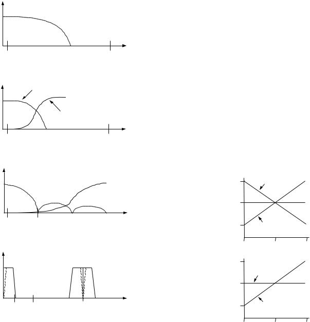
The AD73322L’s input channels employ a sigma-delta conversion technique, which provides a high resolution 16-bit output with system filtering being implemented on-chip.
Sigma-delta converters employ a technique known as oversampling, where the sampling rate is many times the highest frequency of interest. In the case of the AD73322L, the initial sampling rate of the sigma-delta modulator is DMCLK/8. The main effect of oversampling is that the quantization noise is spread over a very wide bandwidth, up to FS/2 = DMCLK/16 (Figure 7a). This means that the noise in the band of interest is much reduced. Another complementary feature of sigma-delta converters is the use of a technique called noise-shaping. This technique has the effect of pushing the noise from the band of
interest to an out-of-band position (Figure 7b). The combination of these techniques, followed by the application of a digital filter, sufficiently reduces the noise in band to ensure good dynamic performance from the part (Figure 7c).
BAND |
FS/2 |
OF |
|
INTEREST |
DMCLK/16 |
|
a. |
|
NOISE SHAPING |
BAND |
FS/2 |
OF |
|
INTEREST |
DMCLK/16 |
|
b. |
|
DIGITAL FILTER |
BAND |
FS/2 |
OF |
|
INTEREST |
DMCLK/16 |
|
c. |
Figure 6. Sigma-Delta Noise Reduction
Figure 7 shows the various stages of filtering that are employed in a typical AD73322L application. In Figure 7a we see the transfer function of the external analog antialias filter. Even though it is a single RC pole, its cutoff frequency is sufficiently far away from the initial sampling frequency (DMCLK/8) that it takes care of any signals that could be aliased by the sampling frequency. This also shows the major difference between the initial oversampling rate and the bandwidth of interest. In Figure 7b, the signal and noise-shaping responses of the sigma-delta modulator are shown. The signal response provides further rejection of any high frequency signals while the noise-shaping will push the inherent quantization noise to an out-of-band position. The detail of Figure 7c shows the response of the digital decimation filter (Sinc-cubed response) with nulls every multiple of DMCLK/ 256, which corresponds to the decimation filter update rate for a 64 kHz sampling. The nulls of the Sinc3 response correspond with multiples of the chosen sampling frequency. The final detail in Figure 7d shows the application of a final antialias filter in the DSP engine. This has the advantage of being implemented according to the user’s requirements and available MIPS. The filtering in Figures 7a through 7c is implemented in the AD73322L.
REV. 0 |
–11– |
AD73322L
FB = 4kHz |
FSINIT = DMCLK/8 |
a. Analog Antialias Filter Transfer Function
SIGNAL TRANSFER FUNCTION
NOISE TRANSFER FUNCTION
FB = 4kHz |
FSINIT = DMCLK/8 |
b. Analog Sigma-Delta Modulator Transfer Function
FB = 4kHz |
FSINTER = DMCLK/256 |
c. Digital Decimator Transfer Function
FB = 4kHz F |
SFINAL |
= 8kHz |
F |
SINTER |
= DMCLK/256 |
|
|
|
|
d. Final Filter LPF (HPF) Transfer Function
Figure 7. ADC Frequency Responses
Decimation Filter
The digital filter used in the AD73322L carries out two important functions. Firstly, it removes the out-of-band quantization noise, which is shaped by the analog modulator and secondly, it decimates the high frequency bit stream to a lower rate 16bit word.
The antialiasing decimation filter is a sinc-cubed digital filter that reduces the sampling rate from DMCLK/8 to DMCLK/256, and increases the resolution from a single bit to 15 bits or greater (depending on chosen sampling rate). Its Z transform is given as:
[(1 – Z –N)/(1 – Z –1)]3
where N is set by the sampling rate (N = 32 @ 64 kHz sampling. . . N = 256 @ 8 kHz sampling). Thus when the sampling rate is 64 kHz, a minimal group delay of 25 s can be achieved.
Word growth in the decimator is determined by the sampling rate. At 64 kHz sampling, where the oversampling ratio between sigma-delta modulator and decimator output equals 32, there are five bits per stage of the three-stage Sinc3 filter. Due to symmetry within the sigma-delta modulator, the LSB will always be a zero; therefore, the 16-bit ADC output word will have 2 LSBs equal to zero, one due to the sigma-delta symmetry and the other being a padding zero to make up the 16-bit word. At lower sampling rates, decimator word growth will be greater than the 16-bit sample word, therefore truncation occurs in transferring the decimator output as the ADC word. For example, at 8 kHz sampling, word growth reaches 24 bits due to the OSR of 256 between sigma-delta modulator and decimator output. This yields eight bits per stage of the three-stage Sinc3 filter.
ADC Coding
The ADC coding scheme is in twos complement format (see Figure 8). The output words are formed by the decimation filter, which grows the word length from the single-bit output of the sigma-delta modulator to a word length of up to 24 bits (depending on decimation rate chosen), which is the final output of the ADC block. In Data Mode this value is truncated to 16 bits for output on the Serial Data Output (SDO) pin.
VREF + (VREF 0.32875) VINN
ANALOG |
|
|
VREF |
|
|
INPUT |
|
|
|
|
|
V |
REF |
– (V |
REF |
0.32875) |
VINP |
|
|
|
|
||
10... |
00 |
00... |
00 |
01... |
11 |
ADC CODE DIFFERENTIAL
VREF + (VREF 0.6575)
VINN
ANALOG
INPUT
VREF – (VREF 0.6575) |
VINP |
|
10... |
00 |
00... |
00 |
01... |
11 |
ADC CODE SINGLE-ENDED
Figure 8. ADC Transfer Function
In mixed Control/Data Mode, the resolution is fixed at 15 bits, with the MSB of the 16-bit transfer being used as a flag bit to indicate either control or data in the frame.
Decoder Channel
The decoder channels consist of digital interpolators, digital sigma-delta modulators, single-bit digital-to-analog converters (DAC), analog smoothing filters and programmable gain amplifiers with differential outputs.
DAC Coding
The DAC coding scheme is in twos complement format with 0x7FFF being full-scale positive and 0x8000 being fullscale negative.
–12– |
REV. 0 |
Loading...