


 Loading...
|
1 GSPS Quadrature Digital Upconverter |
|
with 18-Bit I/Q Data Path and 14-Bit DAC |
Data Sheet |
AD9957 |
|
|
FEATURES
1 GSPS internal clock speed (up to 400 MHz analog output) Integrated 1 GSPS 14-bit DAC
250 MSPS input data rate
Phase noise ≤ −125 dBc/Hz (400 MHz carrier @ 1 kHz offset) Excellent dynamic performance >80 dB narrow-band SFDR 8 programmable profiles for shift keying
Sin(x)/(x) correction (inverse sinc filter) Reference clock multiplier
Internal oscillator for a single crystal operation Software and hardware controlled power-down Integrated RAM
Phase modulation capability Multichip synchronization
Easy interface to Blackfin SPORT Interpolation factors from 4× to 252× Interpolation DAC mode
Gain control DAC
Internal divider allows references up to 2 GHz 1.8 V and 3.3 V power supplies
100-lead TQFP_EP package
APPLICATIONS
HFC data, telephony, and video modems
Wireless base station transmissions
Broadband communications transmissions
Internet telephony
GENERAL DESCRIPTION
The AD9957 functions as a universal I/Q modulator and agile upconverter for communications systems where cost, size, power consumption, and dynamic performance are critical. The AD9957 integrates a high speed, direct digital synthesizer (DDS), a high performance, high speed, 14-bit digital-to-analog converter (DAC), clock multiplier circuitry, digital filters, and other DSP functions onto a single chip. It provides baseband upconversion for data transmission in a wired or wireless communications system.
The AD9957 is the third offering in a family of quadrature digital upconverters (QDUCs) that includes the AD9857 and AD9856. It offers performance gains in operating speed, power consumption, and spectral performance. Unlike its predecessors, it supports a 16-bit serial input mode for I/Q baseband data. The device can alternatively be programmed to operate either as a single tone, sinusoidal source or as an interpolating DAC.
The reference clock input circuitry includes a crystal oscillator, a high speed, divide-by-two input, and a low noise PLL for multiplication of the reference clock frequency.
The user interface to the control functions includes a serial port easily configured to interface to the SPORT of the Blackfin® DSP and profile pins to enable fast and easy shift keying of any signal parameter (phase, frequency, or amplitude).
FUNCTIONAL BLOCK DIAGRAM
|
I |
|
DATA |
|
|
FORMAT AND |
|
||
I/Q DATA |
14-BIT DAC |
FOR |
||
INTERPOLATE |
||||
|
|
|
XMIT |
|
|
Q |
|
|
|
|
NCO |
AD9957 |
|
|
|
TIMING |
|
|
|
|
AND |
REFERENCE CLOCK |
|
|
|
CONTROL |
INPUT CIRCUITRY |
|
|
|
USER INTERFACE |
|
|
|
|
REFERENCE CLOCK INPUT |
|
||
06384-001
Figure 1.
Rev. C
Information furnished by Analog Devices is believed to be accurate and reliable. However, no responsibilityisassumedbyAnalogDevicesforitsuse,norforanyinfringementsofpatentsorother rightsofthirdpartiesthatmayresultfromitsuse.Specificationssubjecttochangewithoutnotice.No license is granted by implication or otherwise under any patent or patent rights of Analog Devices. Trademarksandregisteredtrademarksarethepropertyoftheirrespectiveowners.
One Technology Way, P.O. Box 9106, Norwood, MA 02062-9106, U.S.A. Tel: 781.329.4700 www.analog.com Fax: 781.461.3113 ©2007–2012 Analog Devices, Inc. All rights reserved.

AD9957 |
Data Sheet |
TABLE OF CONTENTS |
|
Features .............................................................................................. |
1 |
Applications....................................................................................... |
1 |
General Description ......................................................................... |
1 |
Functional Block Diagram .............................................................. |
1 |
Revision History ............................................................................... |
4 |
Specifications..................................................................................... |
5 |
Electrical Specifications............................................................... |
5 |
Absolute Maximum Ratings............................................................ |
8 |
ESD Caution.................................................................................. |
8 |
Pin Configuration and Function Descriptions............................. |
9 |
Typical Performance Characteristics ........................................... |
12 |
Modes of Operation ....................................................................... |
16 |
Overview...................................................................................... |
16 |
Quadrature Modulation Mode ................................................. |
17 |
BlackFin Interface (BFI) Mode................................................. |
18 |
Interpolating DAC Mode .......................................................... |
19 |
Single Tone Mode....................................................................... |
20 |
Signal Processing ............................................................................ |
21 |
Parallel Data Clock (PDCLK)................................................... |
21 |
Transmit Enable Pin (TxEnable).............................................. |
21 |
Input Data Assembler ................................................................ |
22 |
Inverse CCI Filter ....................................................................... |
23 |
Fixed Interpolator (4×).............................................................. |
23 |
Programmable Interpolating Filter .......................................... |
24 |
QDUC Mode........................................................................... |
24 |
BFI Mode................................................................................. |
24 |
Quadrature Modulator .............................................................. |
25 |
DDS Core..................................................................................... |
25 |
Inverse Sinc Filter ....................................................................... |
25 |
Output Scale Factor (OSF) ........................................................ |
26 |
14-Bit DAC.................................................................................. |
26 |
Auxiliary DAC ........................................................................ |
26 |
RAM Control .................................................................................. |
27 |
RAM Overview........................................................................... |
27 |
RAM Segment Registers............................................................ |
27 |
RAM State Machine ................................................................... |
27 |
RAM Trigger (RT) Pin............................................................... |
27 |
Load/Retrieve RAM Operation................................................ |
28 |
RAM Playback Operation......................................................... |
28 |
Overview of RAM Playback Modes......................................... |
29 |
RAM Ramp-Up Mode........................................................... |
29 |
RAM Bidirectional Ramp Mode .......................................... |
30 |
RAM Continuous Bidirectional Ramp Mode .................... |
32 |
RAM Continuous Recirculate Mode................................... |
33 |
Clock Input (REF_CLK)................................................................ |
34 |
REFCLK Overview..................................................................... |
34 |
Crystal Driven REF_CLK ......................................................... |
34 |
Direct Driven REF_CLK ........................................................... |
34 |
Phase-Locked Loop (PLL) Multiplier...................................... |
35 |
PLL Charge Pump ...................................................................... |
36 |
External PLL Loop Filter Components ................................... |
36 |
PLL Lock Indication .................................................................. |
36 |
Additional Features ........................................................................ |
37 |
Output Shift Keying (OSK)....................................................... |
37 |
Manual OSK............................................................................ |
37 |
Automatic OSK....................................................................... |
37 |
Profiles ......................................................................................... |
38 |
I/O_UPDATE Pin ...................................................................... |
38 |
Automatic I/O Update ............................................................... |
38 |
Power-Down Control ................................................................ |
39 |
General-Purpose I/O (GPIO) Port .......................................... |
39 |
Synchronization of Multiple Devices........................................... |
40 |
Overview ..................................................................................... |
40 |
Clock Generator ......................................................................... |
40 |
Rev. C | Page 2 of 64

Data Sheet |
AD9957 |
Sync Generator ............................................................................ |
40 |
Sync Receiver ............................................................................... |
41 |
Setup/Hold Validation................................................................ |
42 |
Synchronization Example .......................................................... |
44 |
I/Q Path Latency ......................................................................... |
45 |
Example.................................................................................... |
45 |
Power Supply Partitioning ............................................................. |
46 |
3.3 V Supplies .............................................................................. |
46 |
DVDD_I/O (Pin 11, Pin 15, Pin 21, Pin 28, Pin 45, Pin 56, |
|
Pin 66) ...................................................................................... |
46 |
AVDD (Pin 74 to Pin 77 and Pin 83) ................................... |
46 |
1.8 V Supplies .............................................................................. |
46 |
DVDD (Pin 17, Pin 23, Pin 30, Pin 47, Pin 57, Pin 64) ..... |
46 |
AVDD (Pin 3).......................................................................... |
46 |
AVDD (Pin 6).......................................................................... |
46 |
AVDD (Pin 89 and Pin 92).................................................... |
46 |
Serial Programming........................................................................ |
47 |
Control Interface—Serial I/O.................................................... |
47 |
General Serial I/O Operation .................................................... |
47 |
Instruction Byte........................................................................... |
47 |
Instruction Byte Information Bit Map ................................. |
47 |
Serial I/O Port Pin Descriptions ............................................... |
47 |
SCLK—Serial Clock................................................................ |
47 |
CS—Chip Select Bar ............................................................... |
47 |
SDIO—Serial Data Input/Output......................................... |
47 |
SDO—Serial Data Out ........................................................... |
48 |
I/O_RESET—Input/Output Reset........................................ |
48 |
I/O_UPDATE—Input/Output Update ................................ |
48 |
Serial I/O Timing Diagrams...................................................... |
48 |
MSB/LSB Transfers..................................................................... |
48 |
I/O_UPDATE, SYNC_CLK, and System Clock |
|
Relationships................................................................................ |
49 |
Register Map and Bit Descriptions ............................................... |
50 |
Register Map................................................................................ |
50 |
Register Bit Descriptions............................................................ |
55 |
Control Function Register 1 (CFR1).................................... |
55 |
Control Function Register 2 (CFR2).................................... |
56 |
Control Function Register 3 (CFR3).................................... |
58 |
Auxiliary DAC Control Register........................................... |
58 |
I/O Update Rate Register....................................................... |
58 |
RAM Segment Register 0....................................................... |
58 |
RAM Segment Register 1....................................................... |
59 |
Amplitude Scale Factor (ASF) Register ............................... |
59 |
Multichip Sync Register ......................................................... |
59 |
Profile Registers........................................................................... |
60 |
Profile<7:0> Register—Single Tone...................................... |
60 |
Profile<7:0> Register—QDUC ............................................. |
60 |
RAM Register .......................................................................... |
60 |
GPIO Configuration Register ............................................... |
60 |
GPIO Data Register ................................................................ |
60 |
Outline Dimensions........................................................................ |
61 |
Ordering Guide ........................................................................... |
61 |
Rev. C | Page 3 of 64
AD9957 |
Data Sheet |
|
|
REVISION HISTORY |
|
4/12—Rev. B to Rev. C |
|
Changes to Table 1............................................................................ |
7 |
Changes to Table 3.......................................................................... |
11 |
Change to Sync Generator Section............................................... |
41 |
Changes to Sync Receiver Section and Setup/Hold Validation |
|
Section.............................................................................................. |
42 |
Changes to Table 13........................................................................ |
50 |
Changes to Table 19........................................................................ |
57 |
Changes to Table 26........................................................................ |
59 |
10/10—Rev. A to Rev. B |
|
Changes to Data Rate in Features Section..................................... |
1 |
Changes to Specifications Section.................................................. |
6 |
Added EPAD Notation to Figure 4 and Table 3 ........................... |
9 |
Changes to XTAL_SEL Pin Description...................................... |
11 |
Changes to BlackFin Interface (BFI) Mode Section .................. |
18 |
Changes to Figure 30 and Figure 31............................................. |
22 |
Changes to Programmable Interpolating Filter Section............ |
24 |
Changes to Fifth Paragraph of Quadrature Modulator Section...... |
25 |
Changes to RAM Segment Registers Section ............................. |
27 |
Changes to RAM Playback Operation Section........................... |
28 |
Changes to Control Interface—Serial I/O Section..................... |
47 |
Added to I/O_UPDATE, SYNC_CLK, and System Clock |
|
Relationships Section and Figure 64 ............................................ |
49 |
Changes to Default Values of Profile 0 Register—Single Tone |
|
(0x0E) and Profile 0 Register—QDUC (0x0E) in Table 14....... |
51 |
Changes to Default Values in Table 15......................................... |
52 |
Changes to Default Values in Table 16......................................... |
53 |
Changes to Default Values in Table 17......................................... |
54 |
Updated Outline Dimensions ....................................................... |
61 |
1/08—Rev. 0 to Rev. A |
|
Changes to REFCLK Multiplier Specification............................... |
3 |
Changes to I/O_Update/Profile<2:0>/RT Timing |
|
Characteristics and I/Q Input Timing Characteristics................. |
5 |
Replaced Pin Configuration and Function Descriptions |
|
Section................................................................................................. |
8 |
Changes to Figure 25 Through Figure 29.................................... |
15 |
Deleted Table 4, Renumbered Sequentially ................................ |
20 |
Changes to DDS Core Section...................................................... |
24 |
Changes to Figure 47 and Table 6................................................. |
33 |
Replaced Synchronization of Multiple Devices Section............ |
39 |
Added I/Q Path Latency Section.................................................. |
44 |
Added Power Supply Partitioning Section.................................. |
45 |
Changes to General Serial I/O Operation Section..................... |
46 |
Changes to Table 13 ....................................................................... |
48 |
Changes to Table 14 ....................................................................... |
49 |
Changes to Table 19 ....................................................................... |
54 |
Changes to Table 20 ....................................................................... |
56 |
Changes to GPIO Configuration Register and |
|
GPIO Data Register Sections ........................................................ |
58 |
5/07—Revision 0: Initial Version |
|
Rev. C | Page 4 of 64

Data Sheet |
AD9957 |
SPECIFICATIONS
ELECTRICAL SPECIFICATIONS
AVDD (1.8V) and DVDD (1.8V) = 1.8 V ± 5%, AVDD (3.3V) = 3.3 V ± 5%, DVDD_I/O (3.3V) = 3.3 V ± 5%, T = 25°C, RSET = 10 kΩ, IOUT = 20 mA, external reference clock frequency = 1000 MHz with REFCLK multiplier disabled, unless otherwise noted.
Table 1.
Parameter |
Test Conditions/Comments |
Min |
Typ |
Max |
Unit |
REF_CLK INPUT CHARACTERISTICS |
|
|
|
|
|
Frequency Range |
|
|
|
|
|
REFCLK Multiplier |
Disabled |
60 |
|
10001 |
MHz |
|
Enabled |
3.2 |
|
60 |
MHz |
Maximum REFCLK Input Divider Frequency |
Full temperature range |
1500 |
1900 |
|
MHz |
Minimum REFCLK Input Divider Frequency |
Full temperature range |
|
25 |
35 |
MHz |
External Crystal |
|
|
25 |
|
MHz |
Input Capacitance |
|
|
3 |
|
pF |
Input Impedance (Differential) |
|
|
2.8 |
|
kΩ |
Input Impedance (Single-Ended) |
|
|
1.4 |
|
kΩ |
Duty Cycle |
REFCLK multiplier disabled |
45 |
|
55 |
% |
|
REFCLK multiplier enabled |
40 |
|
60 |
% |
REF_CLK Input Level |
Single-ended |
50 |
|
1000 |
mV p-p |
|
Differential |
100 |
|
2000 |
mV p-p |
REFCLK MULTIPLIER VCO GAIN CHARACTERISTICS |
|
|
|
|
|
VCO Gain (KV) @ Center Frequency |
VCO0 range setting |
|
429 |
|
MHz/V |
|
VCO1 range setting |
|
500 |
|
MHz/V |
|
VCO2 range setting |
|
555 |
|
MHz/V |
|
VCO3 range setting |
|
750 |
|
MHz/V |
|
VCO4 range setting |
|
789 |
|
MHz/V |
|
VCO5 range setting2 |
|
850 |
|
MHz/V |
REFCLK_OUT CHARACTERISTICS |
|
|
|
|
|
Maximum Capacitive Load |
|
|
20 |
|
pF |
Maximum Frequency |
|
|
25 |
|
MHz |
|
|
|
|
|
|
DAC OUTPUT CHARACTERISTICS |
|
|
|
|
|
Full-Scale Output Current |
|
8.6 |
20 |
31.6 |
mA |
Gain Error |
|
−10 |
|
+10 |
%FS |
Output Offset |
|
|
|
2.3 |
µA |
Differential Nonlinearity |
|
|
0.8 |
|
LSB |
Integral Nonlinearity |
|
|
1.5 |
|
LSB |
Output Capacitance |
|
|
5 |
|
pF |
Residual Phase Noise |
@ 1 kHz Offset, 20 MHz AOUT |
|
|
|
|
REFCLK Multiplier |
Disabled |
|
−152 |
|
dBc/Hz |
|
Enabled @ 20× |
|
−140 |
|
dBc/Hz |
|
Enabled @ 100× |
|
−140 |
|
dBc/Hz |
AC Voltage Compliance Range |
|
−0.5 |
|
+0.5 |
V |
|
|
|
|
|
|
SPURIOUS-FREE DYNAMIC RANGE (SFDR SINGLE TONE) |
|
|
|
|
|
fOUT = 20.1 MHz |
|
|
−70 |
|
dBc |
fOUT = 98.6 MHz |
|
|
−69 |
|
dBc |
fOUT = 201.1 MHz |
|
|
−61 |
|
dBc |
fOUT = 397.8 MHz |
|
|
−54 |
|
dBc |
Rev. C | Page 5 of 64
AD9957 |
|
|
Data Sheet |
|
|
|
|
|
|
|
|
|
|
|
Parameter |
Test Conditions/Comments |
Min Typ Max |
|
Unit |
NOISE SPECTRAL DENSITY (NSD) |
|
|
|
|
Single Tone |
|
|
|
|
fOUT = 20.1 MHz |
|
−167 |
|
dBm/Hz |
fOUT = 98.6 MHz |
|
−162 |
|
dBm/Hz |
fOUT = 201.1 MHz |
|
−157 |
|
dBm/Hz |
fOUT = 397.8 MHz |
|
−151 |
|
dBm/Hz |
TWO-TONE INTERMODULATION DISTORTION (IMD) |
I/Q rate = 62.5 MSPS; 16× interpolation |
|
|
|
fOUT = 25 MHz |
|
−82 |
|
dBc |
fOUT = 50 MHz |
|
−78 |
|
dBc |
fOUT = 100 MHz |
|
−73 |
|
dBc |
MODULATOR CHARACTERISTICS |
|
|
|
|
Input Data |
|
|
|
|
Error Vector Magnitude |
2.5 Msymbols/s, QPSK, 4× oversampled |
0.53 |
|
% |
|
270.8333 ksymbols/s, GMSK, 32× |
0.77 |
|
% |
|
oversampled |
|
|
|
|
2.5 Msymbols/s, 256-QAM, 4× |
0.35 |
|
% |
|
oversampled |
|
|
|
WCDMA—FDD (TM1), 3.84 MHz Bandwidth, |
|
|
|
|
5 MHz Channel Spacing |
|
|
|
|
Adjacent Channel Leakage Ratio (ACLR) |
IF = 143.88 MHz |
−78 |
|
dBc |
Carrier Feedthrough |
|
−78 |
|
dBc |
|
|
|
|
|
SERIAL PORT TIMING CHARACTERISTICS |
|
|
|
|
Maximum SCLK Frequency |
|
70 |
|
Mbps |
Minimum SCLK Pulse Width |
Low |
4 |
|
ns |
|
High |
4 |
|
ns |
Maximum SCLK Rise/Fall Time |
|
2 |
|
ns |
Minimum Data Setup Time to SCLK |
|
5 |
|
ns |
Minimum Data Hold Time to SCLK |
|
0 |
|
ns |
Maximum Data Valid Time in Read Mode |
|
11 |
|
ns |
I/O_UPDATE/PROFILE<2:0>/RT TIMING CHARACTERISTICS |
|
|
|
|
Minimum Pulse Width |
High |
1 |
|
SYNC_CLK |
|
|
|
|
cycle |
Minimum Setup Time to SYNC_CLK |
|
1.75 |
|
ns |
Minimum Hold Time to SYNC_CLK |
|
0 |
|
ns |
|
|
|
|
|
I/Q INPUT TIMING CHARACTERISTICS |
|
|
|
|
Maximum PDCLK Frequency |
|
250 |
|
MHz |
Minimum I/Q Data Setup Time to PDCLK |
|
1.75 |
|
ns |
Minimum I/Q Data Hold Time to PDCLK |
|
0 |
|
ns |
Minimum TxEnable Setup Time to PDCLK |
|
1.75 |
|
ns |
Minimum TxEnable Hold Time to PDCLK |
|
0 |
|
ns |
|
|
|
|
|
MISCELLANEOUS TIMING CHARACTERISTICS |
|
|
|
|
Wake-Up Time3 |
|
1 |
|
|
Fast Recovery Mode |
|
8 |
|
SYSCLK cycles4 |
Full Sleep Mode |
|
150 |
|
μs |
Minimum Reset Pulse Width High |
|
5 |
|
SYSCLK cycles4 |
DATA LATENCY (PIPELINE DELAY) |
|
|
|
|
Data Latency Single Tone Mode |
|
|
|
|
Frequency, Phase-to-DAC Output |
|
79 |
|
SYSCLK cycles4 |
Rev. C | Page 6 of 64
Data Sheet |
|
|
|
AD9957 |
|
|
|
|
|
|
|
|
|
|
Parameter |
Test Conditions/Comments |
Min Typ |
Max |
Unit |
CMOS LOGIC INPUTS |
|
|
|
|
Voltage |
|
|
|
|
Logic 1 |
|
2.0 |
|
V |
Logic 0 |
|
|
0.8 |
V |
Current |
|
|
|
|
Logic 1 |
|
90 |
150 |
µA |
Logic 0 |
|
90 |
150 |
µA |
Input Capacitance |
|
2 |
|
pF |
|
|
|
|
|
XTAL_SEL INPUT |
|
|
|
|
Logic 1 Voltage |
|
1.25 |
|
V |
Logic 0 Voltage |
|
|
0.6 |
V |
Input Capacitance |
|
2 |
|
pF |
|
|
|
|
|
CMOS LOGIC OUTPUTS |
1 mA load |
|
|
|
Voltage |
|
|
|
|
Logic 1 |
|
2.8 |
|
V |
Logic 0 |
|
|
0.4 |
V |
POWER SUPPLY CURRENT |
|
|
|
|
DVDD_I/O (3.3V) Pin Current Consumption |
QDUC mode |
16 |
|
mA |
DVDD (1.8V) Pin Current Consumption |
QDUC mode |
610 |
|
mA |
AVDD (3.3V) Pin Current Consumption |
QDUC mode |
28 |
|
mA |
AVDD (1.8V) Pin Current Consumption |
QDUC mode |
105 |
|
mA |
POWER CONSUMPTION |
|
|
|
|
Single Tone Mode |
|
800 |
|
mW |
Continuous Modulation |
8× interpolation |
1400 |
1800 |
mW |
Inverse Sinc Filter Power Consumption |
|
150 |
200 |
mW |
Full Sleep Mode |
|
12 |
40 |
mW |
|
|
|
|
|
1The system clock is limited to 750 MHz maximum in BFI mode.
2The gain value for VCO range Setting 5 is measured at 1000 MHz.
3Wake-up time refers to the recovery from analog power-down modes. The longest time required is for the Reference Clock Multiplier PLL to relock to the reference.
4SYSCLK cycle refers to the actual clock frequency used on-chip by the DDS. If the reference clock multiplier is used to multiply the external reference clock frequency, the SYSCLK frequency is the external frequency multiplied by the reference clock multiplication factor. If the reference clock multiplier and divider are not used, the SYSCLK frequency is the same as the external reference clock frequency.
Rev. C | Page 7 of 64
AD9957
ABSOLUTE MAXIMUM RATINGS
Table 2.
Parameter |
Rating |
AVDD (1.8V), DVDD (1.8V) Supplies |
2 V |
AVDD (3.3V), DVDD_I/O (3.3V) Supplies |
4 V |
Digital Input Voltage |
−0.7 V to +4 V |
XTAL_SEL |
−0.7 V to +2.2 V |
Digital Output Current |
5 mA |
Storage Temperature Range |
−65°C to +150°C |
Operating Temperature Range |
−40°C to +85°C |
θJA |
22°C/W |
θJC |
2.8°C/W |
Maximum Junction Temperature |
150°C |
Lead Temperature, Soldering (10 sec) |
300°C |
|
|
Stresses above those listed under Absolute Maximum Ratings may cause permanent damage to the device. This is a stress rating only; functional operation of the device at these or any other conditions above those indicated in the operational section of this specification is not implied. Exposure to absolute maximum rating conditions for extended periods may affect device reliability.
Data Sheet
DIGITAL INPUTS
DVDD_I/O
INPUT
AVOID OVERDRIVING DIGITAL INPUTS. |
|
|
FORWARD BIASING ESD DIODES MAY |
-003 |
|
COUPLE DIGITAL NOISE ONTO POWER |
||
06384 |
||
PINS. |
||
|
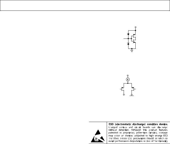
Figure 2. Equivalent Input Circuit
DAC OUTPUTS
AVDD
IOUT IOUT
MUST TERMINATE OUTPUTS TO AGND |
|
|
FOR CURRENT FLOW. DO NOT EXCEED |
-055 |
|
THE OUTPUT VOLTAGE COMPLIANCE |
||
06384 |
||
RATING. |
||
|
Figure 3. Equivalent Output Circuit
ESD CAUTION
Rev. C | Page 8 of 64

Data Sheet |
AD9957 |
PIN CONFIGURATION AND FUNCTION DESCRIPTIONS
|
|
|
NC NC |
|
NC |
|
NC |
|
AGND XTAL SEL |
REFCLK OUT |
|
NC |
|
AVDD (1.8V) |
|
|
REF CLK |
AVDD (1.8V) |
AGND |
NC |
|
NC |
|
AGND |
DAC RSET |
AVDD (3.3V) |
AGND |
|
IOUT |
|
IOUT |
AGND |
|
AGND |
AVDD (3.3V) |
|
AVDD (3.3V) |
||||||||||
|
|
|
|
|
|
|
|
|
REF CLK |
|
|
|
|
|
|
||||||||||||||||||||||||||||||||
|
|
|
|
|
|
|
|
|
|
|
|
|
|
|
|||||||||||||||||||||||||||||||||
|
|
|
|
|
|
|
|
|
|
|
|
|
|
|
|
|
|
|
|
|
|
|
|
|
|
|
|
|
|
|
|
|
|
|
|
|
|
|
|
|
|
|
|
|
|
|
|
|
|
100 |
|
99 |
|
98 |
|
97 |
|
96 |
|
95 |
|
94 |
|
93 |
|
92 |
|
91 |
|
90 |
|
89 |
|
88 |
87 |
|
86 |
|
85 |
84 |
|
83 |
82 |
|
81 |
|
|
80 |
79 |
|
78 |
77 |
|
76 |
|
NC |
|
|
|
|
|
|
|
|
|
|
|
|
|
|
|
|
|
|
|
|
|
|
|
|
|
|
|
|
|
|
|
|
|
|
|
|
|
|
|
|
|
|
|
|
|
|
|
|
|
|
|
|
|
|
|
|
|
|
|
|
|
|
|
|
|
|
|
|
|
|
|
|
|
|
|
|
|
|
|
|
|
|
|
|
|
|
|
|
|
|
|
|
|
|
|
1 |
|
|
|
PIN 1 |
|
|
|
|
|
|
|
|
|
|
|
|
|
|
|
|
|
|
|
|
|
|
|
|
|
|
|
|
|
|
|
|
|
|
|
|
|
|
|
|
|||
PLL_LOOP_FILTER |
|
|
|
|
|
|
|
|
|
|
|
|
|
|
|
|
|
|
|
|
|
|
|
|
|
|
|
|
|
|
|
|
|
|
|
|
|
|
|
|
|
|
|
|
|||
2 |
|
|
|
INDICATOR |
|
|
|
|
|
|
|
|
|
|
|
|
|
|
|
|
|
|
|
|
|
|
|
|
|
|
|
|
|
|
|
|
|
|
|
|
|||||||
AVDD (1.8V) |
|
|
|
|
|
|
|
|
|
|
|
|
|
|
|
|
|
|
|
|
|
|
|
|
|
|
|
|
|
|
|
|
|
|
|
|
|
|
|
|
|
|
|
|
|
|
|
3 |
|
|
|
|
|
|
|
|
|
|
|
|
|
|
|
|
|
|
|
|
|
|
|
|
|
|
|
|
|
|
|
|
|
|
|
|
|
|
|
|
|
|
|
|
|
|
|
AGND |
|
|
|
|
|
|
|
|
|
|
|
|
|
|
|
|
|
|
|
|
|
|
|
|
|
|
|
|
|
|
|
|
|
|
|
|
|
|
|
|
|
|
|
|
|
|
|
4 |
|
|
|
|
|
|
|
|
|
|
|
|
|
|
|
|
|
|
|
|
|
|
|
|
|
|
|
|
|
|
|
|
|
|
|
|
|
|
|
|
|
|
|
|
|
|
|
AGND |
|
|
|
|
|
|
|
|
|
|
|
|
|
|
|
|
|
|
|
|
|
|
|
|
|
|
|
|
|
|
|
|
|
|
|
|
|
|
|
|
|
|
|
|
|
|
|
5 |
|
|
|
|
|
|
|
|
|
|
|
|
|
|
|
|
|
|
|
|
|
|
|
|
|
|
|
|
|
|
|
|
|
|
|
|
|
|
|
|
|
|
|
|
|
|
|
AVDD (1.8V) |
|
|
|
|
|
|
|
|
|
|
|
|
|
|
|
|
|
|
|
|
|
|
|
|
|
|
|
|
|
|
|
|
|
|
|
|
|
|
|
|
|
|
|
|
|
|
|
6 |
|
|
|
|
|
|
|
|
|
|
|
|
|
|
|
|
|
|
|
|
|
|
|
|
|
|
|
|
|
|
|
|
|
|
|
|
|
|
|
|
|
|
|
|
|
|
|
SYNC_IN+ |
|
|
|
|
|
|
|
|
|
|
|
|
|
|
|
|
|
|
|
|
|
|
|
|
|
|
|
|
|
|
|
|
|
|
|
|
|
|
|
|
|
|
|
|
|
|
|
7 |
|
|
|
|
|
|
|
|
|
|
|
|
|
|
|
|
|
|
|
|
|
|
|
|
|
|
|
|
|
|
|
|
|
|
|
|
|
|
|
|
|
|
|
|
|
|
|
SYNC_IN– |
|
|
|
|
|
|
|
|
|
|
|
|
|
|
|
|
|
|
|
|
|
|
|
|
|
|
|
|
|
|
|
|
|
|
|
|
|
|
|
|
|
|
|
|
|
|
|
8 |
|
|
|
|
|
|
|
|
|
|
|
|
|
|
|
|
|
|
|
|
|
|
|
|
|
|
|
|
|
|
|
|
|
|
|
|
|
|
|
|
|
|
|
|
|
|
|
SYNC_OUT+ |
|
|
|
|
|
|
|
|
|
|
|
|
|
|
|
|
|
|
|
|
|
|
|
|
|
|
|
|
|
|
|
|
|
|
|
|
|
|
|
|
|
|
|
|
|
|
|
9 |
|
|
|
|
|
|
|
|
|
|
|
|
|
|
|
|
|
|
|
|
|
|
|
|
|
|
|
|
|
|
|
|
|
|
|
|
|
|
|
|
|
|
|
|
|
|
|
SYNC_OUT– |
|
|
|
|
|
|
|
|
|
|
|
|
|
|
|
|
|
|
|
|
|
|
|
|
|
|
|
|
|
|
|
|
|
|
|
|
|
|
|
|
|
|
|
|
|
|
|
10 |
|
|
|
|
|
|
|
|
|
|
|
|
|
|
|
|
|
|
|
|
|
|
|
|
|
|
|
|
|
|
|
|
|
|
|
|
|
|
|
|
|
|
|
|
|
|
|
DVDD_I/O (3.3V) |
|
|
|
|
|
|
|
|
|
|
|
|
|
|
|
|
|
|
|
|
|
|
|
|
|
|
|
|
|
|
|
|
|
|
|
|
|
|
|
|
|
|
|
|
|
|
|
11 |
|
|
|
|
|
|
|
|
|
|
|
|
|
|
|
|
|
|
|
|
|
|
|
AD9957 |
|
|
|
|
|
|
|
|
|
|
|
|
|
|
|
|
|
||||||
SYNC_SMP_ERR |
|
|
|
|
|
|
|
|
|
|
|
|
|
|
|
|
|
|
|
|
|
|
|
|
|
|
|
|
|
|
|
|
|
|
|
|
|
|
|
|
|
||||||
12 |
|
|
|
|
|
|
|
|
|
|
|
|
|
|
|
|
|
|
|
|
|
TQFP-100 (E_PAD) |
|
|
|
|
|
|
|
|
|
|
|
|
|
|
|
||||||||||
DGND |
|
|
|
|
|
|
|
|
|
|
|
|
|
|
|
|
|
|
|
|
|
|
|
|
|
|
|
|
|
|
|
|
|
|
|
|
|
||||||||||
13 |
|
|
|
|
|
|
|
|
|
|
|
|
|
|
|
|
|
|
|
|
|
|
|
TOP VIEW |
|
|
|
|
|
|
|
|
|
|
|
|
|
|
|
|
|
||||||
|
|
|
|
|
|
|
|
|
|
|
|
|
|
|
|
|
|
|
|
|
|
|
|
|
|
|
|
|
|
|
|
|
|
|
|
|
|
|
|
||||||||
MASTER_RESET |
14 |
|
|
|
|
|
|
|
|
|
|
|
|
|
|
|
|
|
|
|
|
|
|
(Not to Scale) |
|
|
|
|
|
|
|
|
|
|
|
|
|
|
|
|
|
||||||
DVDD_I/O (3.3V) |
|
|
|
|
|
|
|
|
|
|
|
|
|
|
|
|
|
|
|
|
|
|
|
|
|
|
|
|
|
|
|
|
|
|
|
|
|
|
|
|
|
|
|
|
|
|
|
15 |
|
|
|
|
|
|
|
|
|
|
|
|
|
|
|
|
|
|
|
|
|
|
|
|
|
|
|
|
|
|
|
|
|
|
|
|
|
|
|
|
|
|
|
|
|
|
|
DGND |
|
|
|
|
|
|
|
|
|
|
|
|
|
|
|
|
|
|
|
|
|
|
|
|
|
|
|
|
|
|
|
|
|
|
|
|
|
|
|
|
|
|
|
|
|
|
|
16 |
|
|
|
|
|
|
|
|
|
|
|
|
|
|
|
|
|
|
|
|
|
|
|
|
|
|
|
|
|
|
|
|
|
|
|
|
|
|
|
|
|
|
|
|
|||
DVDD (1.8V) |
|
|
|
|
|
|
|
|
|
|
|
|
|
|
|
|
|
|
|
|
|
|
|
|
|
|
|
|
|
|
|
|
|
|
|
|
|
|
|
|
|
|
|
|
|
|
|
17 |
|
|
|
|
|
|
|
|
|
|
|
|
|
|
|
|
|
|
|
|
|
|
|
|
|
|
|
|
|
|
|
|
|
|
|
|
|
|
|
|
|
|
|
|
|
|
|
EXT_PWR_DWN |
|
|
|
|
|
|
|
|
|
|
|
|
|
|
|
|
|
|
|
|
|
|
|
|
|
|
|
|
|
|
|
|
|
|
|
|
|
|
|
|
|
|
|
|
|
|
|
18 |
|
|
|
|
|
|
|
|
|
|
|
|
|
|
|
|
|
|
|
|
|
|
|
|
|
|
|
|
|
|
|
|
|
|
|
|
|
|
|
|
|
|
|
|
|||
PLL_LOCK |
|
|
|
|
|
|
|
|
|
|
|
|
|
|
|
|
|
|
|
|
|
|
|
|
|
|
|
|
|
|
|
|
|
|
|
|
|
|
|
|
|
|
|
|
|
|
|
19 |
|
|
|
|
|
|
|
|
|
|
|
|
|
|
|
|
|
|
|
|
|
|
|
|
|
|
|
|
|
|
|
|
|
|
|
|
|
|
|
|
|
|
|
|
|||
CCI_OVFL |
|
|
|
|
|
|
|
|
|
|
|
|
|
|
|
|
|
|
|
|
|
|
|
|
|
|
|
|
|
|
|
|
|
|
|
|
|
|
|
|
|
|
|
|
|
|
|
20 |
|
|
|
|
|
|
|
|
|
|
|
|
|
|
|
|
|
|
|
|
|
|
|
|
|
|
|
|
|
|
|
|
|
|
|
|
|
|
|
|
|
|
|
|
|
|
|
DVDD_I/O (3.3V) |
|
|
|
|
|
|
|
|
|
|
|
|
|
|
|
|
|
|
|
|
|
|
|
|
|
|
|
|
|
|
|
|
|
|
|
|
|
|
|
|
|
|
|
|
|
|
|
21 |
|
|
|
|
|
|
|
|
|
|
|
|
|
|
|
|
|
|
|
|
|
|
|
|
|
|
|
|
|
|
|
|
|
|
|
|
|
|
|
|
|
|
|
|
|
|
|
DGND |
|
|
|
|
|
|
|
|
|
|
|
|
|
|
|
|
|
|
|
|
|
|
|
|
|
|
|
|
|
|
|
|
|
|
|
|
|
|
|
|
|
|
|
|
|
|
|
22 |
|
|
|
|
|
|
|
|
|
|
|
|
|
|
|
|
|
|
|
|
|
|
|
|
|
|
|
|
|
|
|
|
|
|
|
|
|
|
|
|
|
|
|
|
|
|
|
DVDD (1.8V) |
|
|
|
|
|
|
|
|
|
|
|
|
|
|
|
|
|
|
|
|
|
|
|
|
|
|
|
|
|
|
|
|
|
|
|
|
|
|
|
|
|
|
|
|
|
|
|
23 |
|
|
|
|
|
|
|
|
|
|
|
|
|
|
|
|
|
|
|
|
|
|
|
|
|
|
|
|
|
|
|
|
|
|
|
|
|
|
|
|
|
|
|
|
|
|
|
NC |
|
|
|
|
|
|
|
|
|
|
|
|
|
|
|
|
|
|
|
|
|
|
|
|
|
|
|
|
|
|
|
|
|
|
|
|
|
|
|
|
|
|
|
|
|
|
|
24 |
|
|
|
|
|
|
|
|
|
|
|
|
|
|
|
|
|
|
|
|
|
|
|
|
|
|
|
|
|
|
|
|
|
|
|
|
|
|
|
|
|
|
|
|
|
|
|
D17 |
|
|
|
|
|
|
|
|
|
|
|
|
|
|
|
|
|
|
|
|
|
|
|
|
|
|
|
|
|
|
|
|
|
|
|
|
|
|
|
|
|
|
|
|
|
|
|
25 |
|
|
|
|
|
|
|
|
|
|
|
|
|
|
|
|
|
|
|
|
|
|
|
|
|
|
|
|
|
|
|
|
|
|
|
|
|
|
|
|
|
|
|
|
|
|
|
|
|
|
|
|
|
|
|
|
|
|
|
|
|
|
|
|
|
|
|
|
|
|
|
|
|
|
|
|
|
|
|
|
|
|
|
|
|
|
|
|
|
|
|
|
|
|
|
|
|
|
26 |
|
27 |
|
28 |
29 |
|
30 |
|
31 |
|
32 |
|
33 |
|
34 |
|
35 |
|
36 |
|
37 |
|
38 |
39 |
|
40 |
|
41 |
42 |
|
43 |
44 |
|
45 |
|
|
46 |
47 |
|
48 |
49 |
|
50 |
|
|
|
|
|
|
|
|
|
|
|
|
|
|
|
|
|
|
|
|
|
|
|
|
|
|
|
|
|
|
|
|
|
|
|
|
|
|
|
|
|
|
|
|
|
|
|
|
|
NOTES |
|
D16 |
D15 |
DVDD I/O (3.3V) |
DGND |
DVDD (1.8V) |
D14 |
D13 |
D12 |
D11 |
D10 |
D9 |
D8 |
D7 |
D6 |
PDCLK |
TxENABLE/FS |
D5/SPORT I-DATA |
D4/SPORT Q-DATA |
D3 |
DVDD I/O (3.3V) |
|
DGND |
DVDD (1.8V) |
D2 |
D1 |
D0 |
||||||||||||||||||||
|
|
|
|
|
|
|
|
|
|
|
|
|
|
|
|
|
|
|
|
|
|
|
|
|
|
|
|
|
|
|
|
|
|
|
|
|
|
|
|
|
|
|
|
|
|
|
|
1.NC = NO CONNECT.
2.EXPOSED PAD SHOULD BE SOLDERED TO GROUND.
Figure 4. Pin Configuration
75 |
AVDD (3.3V) |
||
|
AVDD (3.3V) |
||
74 |
|||
|
AGND |
||
73 |
|||
|
NC |
||
72 |
|||
|
I/O_RESET |
||
71 |
|||
|
|
|
|
70 |
CS |
||
|
SCLK |
||
69 |
|||
|
SDO |
||
68 |
|||
|
SDIO |
||
67 |
|||
|
DVDD_I/O (3.3V) |
||
66 |
|||
|
DGND |
||
65 |
|||
|
DVDD (1.8V) |
||
64 |
|||
|
DGND |
||
63 |
|||
|
DGND |
||
62 |
|||
|
NC |
||
61 |
|||
|
OSK |
||
60 |
|||
|
I/O_UPDATE |
||
59 |
|||
|
DGND |
||
58 |
|||
|
DVDD (1.8V) |
||
57 |
|||
|
DVDD_I/O (3.3V) |
||
56 |
|||
|
SYNC_CLK |
||
55 |
|||
|
PROFILE0 |
||
54 |
|||
|
PROFILE1 |
||
53 |
|||
|
PROFILE2 |
||
52 |
|||
|
RT |
||
51 |
|||
06384-004
Rev. C | Page 9 of 64
AD9957 |
|
|
Data Sheet |
|
|
|
|
Table 3. Pin Function Descriptions |
|
|
|
Pin No. |
Mnemonic |
I/O1 |
Description |
1, 24, 61, 72, 86, |
NC |
|
Not Connected. Allow device pin to float. |
87, 93, 97 to 100 |
|
|
|
2 |
PLL_LOOP_FILTER |
I |
PLL-Loop Filter Compensation. See External PLL Loop Filter Components section. |
3, 6, 89, 92 |
AVDD (1.8V) |
I |
Analog Core VDD. 1.8 V analog supplies. |
74 to 77, 83 |
AVDD (3.3V) |
I |
Analog DAC VDD. 3.3 V analog supplies. |
17, 23, 30, 47, 57, |
DVDD (1.8V) |
I |
Digital Core VDD. 1.8 V digital supplies. |
64 |
|
|
|
11, 15, 21, 28, 45, |
DVDD_I/O (3.3V) |
I |
Digital Input/Output VDD. 3.3 V digital supplies. |
56, 66 |
|
|
|
4, 5, 73, 78, 79, |
AGND |
I |
Analog Ground. |
82, 85, 88, 96 |
|
|
|
13, 16, 22, 29, 46, |
DGND |
I |
Digital Ground. |
58, 62, 63, 65 |
|
|
|
7 |
SYNC_IN+ |
I |
Synchronization Signal, Digital Input (Rising Edge Active). Synchronization signal from |
|
|
|
external master to synchronize internal subclocks. See the Synchronization of Multiple |
|
|
|
Devices section. |
8 |
SYNC_IN− |
I |
Synchronization Signal, Digital Input (Falling Edge Active). Synchronization signal from |
|
|
|
external master to synchronize internal subclocks. See the Synchronization of Multiple |
|
|
|
Devices section. |
9 |
SYNC_OUT+ |
O |
Synchronization Signal, Digital Output (Rising Edge Active). Synchronization signal from |
|
|
|
internal device subclocks to synchronize external slave devices. See the Synchronization of |
|
|
|
Multiple Devices section. |
10 |
SYNC_OUT− |
O |
Synchronization Signal, Digital Output (Falling Edge Active). Synchronization signal from |
|
|
|
internal device subclocks to synchronize external slave devices. See the Synchronization of |
|
|
|
Multiple Devices section. |
12 |
SYNC_SMP_ERR |
O |
Synchronization Sample Error, Digital Output (Active High). A high on this pin indicates |
|
|
|
that the AD9957 did not receive a valid sync signal on SYNC_IN+/SYNC_IN−. See the |
|
|
|
Synchronization of Multiple Devices section. |
14 |
MASTER_RESET |
I |
Master Reset, Digital Input (Active High). This pin clears all memory elements and sets |
|
|
|
registers to default values. |
18 |
EXT_PWR_DWN |
I |
External Power-Down, Digital Input (Active High). A high level on this pin initiates the |
|
|
|
currently programmed power-down mode. See the Power-Down Control section for |
|
|
|
further details. If unused, tie to ground. |
19 |
PLL_LOCK |
O |
PLL Lock, Digital Output (Active High). A high on this pin indicates that the clock multiplier |
|
|
|
PLL has acquired lock to the reference clock input. |
20 |
CCI_OVFL |
O |
CCI Overflow Digital Output, Active High. A high on this pin indicates a CCI filter overflow. |
|
|
|
This pin remains high until the CCI overflow condition is cleared. |
25 to 27, 31 to |
D<17:0> |
I/O |
Parallel Data Input Bus (Active High). These pins provide the interleaved, 18-bit, digital, I |
39, 42 to 44, 48 |
|
|
and Q vectors for the modulator to upconvert. Also used for a GPIO port in Blackfin |
to 50 |
|
|
interface mode. |
42 |
SPORT I-DATA |
I |
In Blackfin interface mode, this pin serves as the I-data serial input. |
43 |
SPORT Q-DATA |
I |
In Blackfin interface mode, this pin serves as the Q-data serial input. |
40 |
PDCLK |
O |
Parallel Data Clock, Digital Output (Clock). See the Signal Processing section for details. |
41 |
TxENABLE/FS |
I |
Transmit Enable, Digital Input (Active High). See the Signal Processing section for details. |
|
|
|
In Blackfin interface mode, this pin serves as the FS input to receive the RFS output signal |
|
|
|
from the Blackfin. |
51 |
RT |
I |
RAM Trigger, Digital Input (Active High). This pin provides control for the RAM amplitude |
|
|
|
scaling function. When this function is engaged, a high sweeps the amplitude from the |
|
|
|
beginning RAM address to the end. A low sweeps the amplitude from the end RAM |
|
|
|
address to the beginning. If unused, connect to ground or supply. |
52 to 54 |
PROFILE<2:0> |
I |
Profile Select Pins, Digital Inputs (Active High). These pins select one of eight |
|
|
|
phase/frequency profiles for the DDS core (single tone or carrier tone). Changing the state |
|
|
|
of one of these pins transfers the current contents of all I/O buffers to the corresponding |
|
|
|
registers. State changes should be set up to the SYNC_CLK pin. |
55 |
SYNC_CLK |
O |
Output System Clock/4, Digital Output (Clock). The I/O_UPDATE and PROFILE<2:0> pins |
|
|
|
should be set up to the rising edge of this signal. |
Rev. C | Page 10 of 64
Data Sheet |
|
|
|
|
|
|
AD9957 |
|
|
|
|
|
|
|
|
|
|
|
|
|
|
|
|
Pin No. |
|
Mnemonic |
I/O1 |
Description |
|||
59 |
|
I/O_UPDATE |
I/O |
Input/Output Update; Digital Input Or Output (Active High) Depending on the Internal I/O |
|||
|
|
|
|
|
|
|
Update Active Bit. A high on this pin indicates a transfer of the contents of the I/O buffers |
|
|
|
|
|
|
|
to the corresponding internal registers. |
60 |
|
OSK |
I |
Output Shift Keying, Digital Input (Active High). When using OSK (manual or automatic), |
|||
|
|
|
|
|
|
|
this pin controls the OSK function. See the Output Shift Keying (OSK) section of the data |
|
|
|
|
|
|
|
sheet for details. When not using OSK, tie this pin high. |
67 |
|
SDIO |
I/O |
Serial Data Input/Output, Digital Input/Output (Active High). This pin can be either |
|||
|
|
|
|
|
|
|
unidirectional or bidirectional (default), depending on configuration settings. In |
|
|
|
|
|
|
|
bidirectional serial port mode, this pin acts as the serial data input and output. In |
|
|
|
|
|
|
|
unidirectional, it is an input only. |
68 |
|
SDO |
O |
Serial Data Output, Digital Output (Active High). This pin is only active in unidirectional |
|||
|
|
|
|
|
|
|
serial data mode. In this mode, it functions as the output. In bidirectional mode, this pin is |
|
|
|
|
|
|
|
not operational and should be left floating. |
69 |
|
SCLK |
I |
Serial Data Clock. Digital clock (rising edge on write, falling edge on read). This pin |
|||
|
|
|
|
|
|
|
provides the serial data clock for the control data path. Write operations to the AD9957 |
|
|
|
|
|
|
|
use the rising edge. Readback operations from the AD9957 use the falling edge. |
70 |
|
|
|
|
I |
Chip Select, Digital Input (Active Low). Bringing this pin low enables the AD9957 to detect |
|
|
CS |
|
|
|
|||
|
|
|
|
|
|
|
serial clock rising/falling edges. Bringing this pin high causes the AD9957 to ignore input |
|
|
|
|
|
|
|
on the serial data pins. |
71 |
|
I/O_RESET |
I |
Input/Output Reset, Digital Input (Active High). Rather than resetting the entire device |
|||
|
|
|
|
|
|
|
during a failed communication cycle, when brought high, this pin resets the state machine |
|
|
|
|
|
|
|
of the serial port controller and clears any I/O buffers that have been written since the last |
|
|
|
|
|
|
|
I/O update. When unused, tie this pin to ground to avoid accidental resets. |
80 |
|
|
|
O |
Open-Source DAC Complementary Output Source. Analog output, current mode. Connect |
||
|
IOUT |
|
|
||||
|
|
|
|
|
|
|
through 50 Ω to AGND. |
81 |
|
IOUT |
O |
Open-Source DAC Output Source. Analog output, current mode. Connect through 50 Ω to |
|||
|
|
|
|
|
|
|
AGND. |
84 |
|
DAC_RSET |
O |
Analog Reference Pin. This pin programs the DAC output full-scale reference current. |
|||
|
|
|
|
|
|
|
Attach a 10 kΩ resistor to AGND. |
90 |
|
REF_CLK |
I |
Reference Clock Input. Analog input. See the REFCLK Overview section for more details. |
|||
91 |
|
|
I |
Complementary Reference Clock Input. Analog input. See the REFCLK Overview section |
|||
|
REF_CLK |
|
|||||
|
|
|
|
|
|
|
for more details. |
94 |
|
REFCLK_OUT |
O |
Reference Clock Output. Analog output. See the REFCLK Overview section for more |
|||
|
|
|
|
|
|
|
details. |
95 |
|
XTAL_SEL |
I |
Crystal Select (1.8 V Logic). Analog input (active high). Driving the XTAL_SEL pin high enables |
|||
|
|
|
|
|
|
|
the internal oscillator to be used with a crystal resonator. If unused, connect it to AGND. |
(EPAD) |
|
Exposed Pad |
|
The EPAD should be soldered to ground. |
|||
|
|
(EPAD) |
|
|
|||
|
|
|
|
|
|
|
|
1 I = input, O = output.
Rev. C | Page 11 of 64

AD9957 |
Data Sheet |
TYPICAL PERFORMANCE CHARACTERISTICS
0 |
1 |
|
|
|
|
–10 |
|
|
–20 |
|
|
–30 |
|
|
–40 |
|
|
–50 |
|
|
–60 |
1 |
|
|
|
|
–70 |
|
|
–80 |
|
|
–90 |
|
-048 |
–100 START 0Hz |
|
06384 |
50MHz/DIV |
STOP 500MHz |
|
Figure 5. 15.625 kHz Quadrature Tone, Carrier = 102 MHz, |
||
|
CCI = 16, fS = 1 GHz |
|
0 |
1 |
|
|
|
|
–10 |
|
|
–20 |
|
|
–30 |
|
|
–40 |
|
|
–50 |
|
|
–60 |
|
1 |
–70 |
|
|
–80 |
|
|
–90 |
|
-050 |
–100 START 0MHz |
|
06384 |
50MHz/DIV |
STOP 500MHz |
|
Figure 6. 15.625 kHz Quadrature Tone, Carrier = 222 MHz, |
||
|
CCI = 16, fS = 1 GHz |
|
0 |
|
1 |
|
|
|
–10 |
|
|
–20 |
|
|
–30 |
|
|
–40 |
|
|
–50 |
1 |
|
|
|
|
–60 |
|
|
–70 |
|
|
–80 |
|
|
–90 |
|
-052 |
–100 START 0Hz |
|
06384 |
50MHz/DIV |
STOP 500MHz |
|
Figure 7. 15.625 kHz Quadrature Tone, Carrier = 372 MHz, |
||
|
CCI = 16, fS = 1 GHz |
|
0 |
|
1 |
|
|
|
–10 |
|
|
–20 |
|
|
–30 |
|
|
–40 |
|
|
–50 |
|
|
–60 |
|
|
–70 |
1 |
|
–80 |
|
|
|
|
|
–90 |
|
-049 |
–100 CENTER 102MHz |
|
06384 |
5kHz/DIV |
SPAN 50kHz |
Figure 8. Narrow-Band View of Figure 5 (with Carrier and Lower Sideband Suppression)
1
0
–10
–20
–30
–40
–50
–60
–70
1
–80
–90 |
|
-051 |
–100 CENTER 222MHz |
|
06384 |
5kHz/DIV |
SPAN 50kHz |
Figure 9. Narrow-Band View of Figure 6 (with Carrier And Lower Sideband Suppression)
1
0
–10
–20
–30
–40
–50
–60
–70 |
1 |
|
–80 |
|
|
|
|
|
–90 |
|
-053 |
–100 CENTER 372MHz |
|
06384 |
5kHz/DIV |
SPAN 50kHz |
Figure 10. Narrow-Band View of Figure 7 (with Carrier and Lower Sideband Suppression)
Rev. C | Page 12 of 64

Data Sheet |
|
|
|
|
AD9957 |
0 |
|
|
0 |
|
|
–10 |
|
|
–10 |
|
|
–20 |
|
|
–20 |
|
|
–30 |
|
|
–30 |
|
|
–40 |
|
|
–40 |
|
|
–50 |
|
|
–50 |
|
|
–60 |
|
|
–60 |
|
|
–70 |
|
|
–70 |
|
|
–80 |
|
-06384044 |
–80 |
|
-06384041 |
–90 |
|
–90 |
|
||
|
|
|
|
||
–100 START 0Hz |
50MHz/DIV |
STOP 500MHz |
–100 CENTER 102MHz |
2MHz/DIV |
SPAN 20MHz |
Figure 11. QPSK, 7.8125 Msymbols/s, 4x Oversampled Raised Cosine, |
|||
|
α = 0.25, CCI = 8, Carrier = 102 MHz, fS = 1 GHz |
||
0 |
|
|
|
–10 |
|
|
|
–20 |
|
|
|
–30 |
|
|
|
–40 |
|
|
|
–50 |
|
|
|
–60 |
|
|
|
–70 |
|
|
|
–80 |
|
|
|
–90 |
|
|
-045 |
–100 |
|
|
06384 |
START 0MHz |
50MHz/DIV |
STOP 500MHz |
|
Figure 12. QPSK, 7.8125 Msymbols/s, 4x Oversampled Raised Cosine, |
|||
|
α = 0.25, CCI = 8, Carrier = 222 MHz, fS = 1 GHz |
||
0 |
|
|
|
–10 |
|
|
|
–20 |
|
|
|
–30 |
|
|
|
–40 |
|
|
|
–50 |
|
|
|
–60 |
|
|
|
–70 |
|
|
|
–80 |
|
|
|
–90 |
|
|
-046 |
–100 |
|
|
06384 |
START 0Hz |
50MHz/DIV |
STOP 500MHz |
|
Figure 13. QPSK, 7.8125 Msymbols/s, 4x Oversampled Raised Cosine, |
|||
|
α = 0.25, CCI = 8, Carrier = 372 MHz, fS = 1 GHz |
||
Figure 14. Narrow-Band View of Figure 11
0 |
|
|
–10 |
|
|
–20 |
|
|
–30 |
|
|
–40 |
|
|
–50 |
|
|
–60 |
|
|
–70 |
|
|
–80 |
|
|
–90 |
|
-042 |
–100 CENTER 222MHz |
|
06384 |
2MHz/DIV |
SPAN 20MHz |
Figure 15. Narrow-Band View of Figure 12
0 |
|
|
–10 |
|
|
–20 |
|
|
–30 |
|
|
–40 |
|
|
–50 |
|
|
–60 |
|
|
–70 |
|
|
–80 |
|
|
–90 |
|
-043 |
–100 CENTER 372MHz |
|
06384 |
2MHz/DIV |
SPAN 20MHz |
Figure 16. Narrow-Band View of Figure 13
Rev. C | Page 13 of 64
AD9957 |
|
|
|
|
|
|
|
|
|
|
–50 |
|
|
|
|
|
|
|
|
|
–55 |
|
|
|
|
|
|
|
|
(dBc)SFDR |
|
SFDR WITHOUT PLL |
|
|
|
|
(dBc/Hz)MAGNITUDE |
||
–60 |
|
|
|
|
|
|
|
||
|
|
|
|
|
|
|
|
|
|
|
–65 |
|
|
|
|
SFDR WITH PLL |
|
||
|
|
|
|
|
|
|
|
|
|
|
–70 |
|
|
|
|
|
|
|
|
|
–75 0 |
|
|
|
|
|
|
|
06384-058 |
|
50 |
100 |
150 |
200 |
250 |
300 |
350 |
400 |
|
|
|
|
|
FREQUENCY OUT (MHz) |
|
|
|
||
Figure 17. Wideband SFDR vs. Output Frequency in Single Tone Mode,
PLL with REFCLK = 15.625 MHz × 64
Data Sheet
–90
–100 fOUT = 397.8MHz
–110  fOUT = 201.1MHz
–120 


 fOUT = 98.6MHz –130


–140
–150 |
–160 fOUT = 20.1MHz |
|
|
|
|
|
-061 |
|
–17010 |
|
|
|
|
|
|
06384 |
100 |
1k |
10k |
100k |
1M |
10M |
100M |
|
|
|
FREQUENCY OFFSET (Hz) |
|
|
|||
Figure 20. Residual Phase Noise, System Clock = 1 GHz
|
–45 |
|
|
|
|
|
|
|
|
|
|
|
|
|
|
|
|
LOW SUPPLY |
|
|
|
|
–50 |
|
|
|
|
|
|
|
|
|
|
|
|
|
|
HIGH SUPPLY |
|
|
|
||
|
–55 |
|
|
|
|
|
|
|
|
|
(dBc) |
–60 |
|
|
|
|
|
|
|
|
|
SFDR |
|
|
|
|
|
|
|
|
|
|
|
|
|
|
|
|
|
|
|
|
|
|
–65 |
|
|
|
|
|
|
|
|
|
|
–70 |
|
|
|
|
|
|
|
|
06384-059 |
|
–75 0 |
|
|
|
|
|
|
|
|
|
|
50 |
100 |
150 |
200 |
250 |
300 |
350 |
400 |
450 |
|
|
|
|
|
FREQUENCY OUT (MHz) |
|
|
|
|||
Figure 18. SFDR vs. Output Frequency and Supply (±5%) in Single Tone Mode, REFCLK = 1 GHz
|
–90 |
|
fOUT = 397.8MHz |
|
|
|
|
|
|
|
|
|
|
|
|
||
|
–100 |
|
|
|
|
|
|
|
Hz) |
–110 |
|
|
fOUT = 201.1MHz |
|
|
|
|
|
|
|
|
|
|
|
|
|
(dBc/ |
–120 |
|
|
|
|
|
|
|
MAGNITUDE |
–130 |
|
|
|
|
|
|
|
–140 |
|
|
|
|
|
|
|
|
|
–150 |
fOUT = 20.1MHz |
|
|
|
|
|
|
|
|
|
|
|
|
|
06384-054 |
|
|
–16010 |
|
|
|
|
fOUT = 98.6MHz |
||
|
100 |
1k |
10k |
100k |
1M |
10M |
100M |
|
|
|
|
FREQUENCY OFFSET (Hz) |
|
|
|||
Figure 21. Residual Phase Noise Using the REFCLK Multiplier, REFCLK = 50 MHz with 20x Multiplication, System Clock = 1 GHz
|
–50 |
|
|
|
|
|
|
|
|
|
|
|
|
|
|
|
–40°C |
|
|
|
|
|
–55 |
|
|
|
|
+85°C |
|
|
|
(mW) |
(dBc)SFDR |
|
|
|
|
|
|
|
|
|
|
–60 |
|
|
|
|
|
|
|
|
DISSIPATIONPOWER |
|
|
|
|
|
|
|
|
|
|
|
|
|
–65 |
|
|
|
|
|
|
|
|
|
|
–70 |
|
|
|
|
|
|
|
|
|
|
–75 0 |
|
|
|
|
|
|
|
|
06384-060 |
|
50 |
100 |
150 |
200 |
250 |
300 |
350 |
400 |
450 |
|
|
|
|
|
FREQUENCY OUT (MHz) |
|
|
|
|||
Figure 19. SFDR vs. Frequency and Temperature in Single Tone Mode, REFCLK = 1 GHz
1200
DVDD 1.8V
1000
800
600
400 |
|
|
|
|
AVDD 1.8V |
|
|
|
||
|
|
|
|
|
|
|
|
|||
|
|
|
|
|
AVDD 3.3V |
|
|
|
||
200 |
|
|
|
|
DVDD 3.3V |
|
|
|
||
|
|
|
|
|
|
|
|
06384-062 |
||
0 |
|
|
|
|
|
|
|
|
||
200 |
300 |
400 |
500 |
600 |
700 |
800 |
900 |
1000 |
||
100 |
||||||||||
SYSTEM CLOCK FREQUENCY (MHz)
Figure 22. Power Dissipation vs. System Clock (PLL Disabled)
Rev. C | Page 14 of 64
Data Sheet |
AD9957 |
|
|
|
1200 |
|
|
|
|
|
|
–20 |
|
|
|
|
|
|
|
|
|
|
1000 |
|
DVDD 1.8V |
|
|
|
|
–30 |
(mW) |
|
|
|
|
|
|
||
|
|
|
|
|
|
|
–40 |
|
800 |
|
|
|
|
|
|
–50 |
|
DISSIPATION |
|
|
|
|
|
|
||
|
|
|
|
|
|
|
–60 |
|
|
|
|
|
|
|
|
|
|
|
600 |
|
|
|
|
|
|
–70 |
|
|
|
|
|
|
|
|
|
POWER |
400 |
|
|
|
|
AVDD 1.8V |
|
–80 |
|
|
|
|
|
–90 |
|||
|
|
|
|
|
|
|
|
|
|
200 |
|
DVDD 3.3V |
AVDD 3.3V |
|
|
–100 |
|
|
|
|
|
|
|
|||
|
|
|
|
|
|
-063 |
||
|
|
|
|
|
|
|
–110 |
|
|
|
|
|
|
|
|
06384 |
|
|
0 |
|
|
|
|
|
|
|
|
500 |
600 |
700 |
800 |
900 |
1000 |
|
|
|
400 |
|
||||||
|
|
|
SYSTEM CLOCK FREQUENCY (MHz) |
|
|
|||
Figure 23. Power Dissipation vs. System Clock (PLL Enabled)
|
|
|
06384-064 |
CENTER 143.86MHz |
2.55MHz/DIV |
SPAN 25.5MHz |
|
Tx CHANNEL |
|
W-CDMA SGFF FWD |
|
BANDWIDTH: 3.84MHz |
POWER: –11.88dBm |
||
ADJACENT CHANNEL |
LOWER: –78.27dB |
||
BANDWIDTH: 3.84MHz |
|||
SPACING: 3MHz |
UPPER: –78.50dB |
||
ADJACENT CHANNEL |
|
|
|
BANDWIDTH: 3.84MHz |
LOWER: –81.42dB |
||
SPACING: 10MHz |
UPPER: –81.87dB |
||
Figure 24. Typical ACLR for Wideband CDMA
Rev. C | Page 15 of 64

AD9957 |
Data Sheet |
MODES OF OPERATION
OVERVIEW
The AD9957 has three basic operating modes.
•Quadrature modulation (QDUC) mode (default)
•Interpolating DAC mode
•Single tone mode
The active mode is selected via the operating mode bits in Control Function Register 1 (CFR1). Single tone mode allows the device to operate as a sinusoidal generator with the DDS driving the DAC directly.
Interpolating DAC mode bypasses the DDS, allowing the user to deliver baseband data to the device at a sample rate lower
than that of the DAC. An internal chain of rate interpolation filters the user data and upsamples to the DAC sample rate. Combined, the filters provide for programmable rate interpolation while suppressing spectral images and retaining the original baseband spectrum.
QDUC mode employs both the DDS and the rate interpolation filters. In this case, two parallel banks of rate interpolation filters allow baseband processing of in-phase and quadrature (I/Q) signals with the DDS providing the carrier signal to be modulated by the baseband signals. A detailed block diagram of the AD9957 is shown in Figure 25.
The inverse sinc filter is available in all three modes.
|
|
|
|
|
|
|
|
(4×) |
63×) |
AD9957 |
|
|
|
|
|
|
|
|
|
|
18 |
|
I |
|
|
|
|
|
|
|
|
|
|
||
|
|
|
16 |
|
|
CCI |
HALFBAND- |
CCI |
|
|
|
|
|
|
|
|
|
|
|
|
|
|
|
|
|
|
|
|
8 |
AUX |
|
||||
|
|
|
|
|
|
INVERSE |
|
FILTERS |
TO(1× |
|
|
|
DAC GAIN |
|
|||
|
|
|
|
IS |
|
|
|
|
|
DDS |
|
|
DAC |
DAC_RSET |
|||
|
18 |
|
|
|
|
|
|
|
|
|
|
|
8-BIT |
||||
I/Q IN |
|
|
|
|
|
|
|
|
|
θ |
|
|
|
|
|||
DATA ASSEMBLERFORMATTERAND |
BLACKFININTERFACE |
|
QS |
|
|
|
|
|
|
|
|
|
|
|
|||
|
|
|
|
|
|
cos (ωt+θ) |
|
|
|
|
DAC |
IOUT |
|||||
|
16 |
|
|
|
|
(4×) |
63×) |
FTW PW |
ω |
|
|
|
|
||||
|
|
|
|
|
|
|
|
|
14-BIT |
IOUT |
|||||||
|
|
|
|
|
|
|
|
|
|
||||||||
|
|
|
|
|
|
sin (ωt+θ) |
|
|
|
|
|
||||||
|
18 |
|
|
CCI |
HALFBAND- |
CCI |
|
SINC |
|
|
|
||||||
|
Q |
CLOCK |
|
|
OUTPUT |
|
|||||||||||
|
|
|
|
|
|||||||||||||
|
|
|
|
|
|
|
SCALE |
|
|||||||||
|
|
|
|
|
|
|
FACTOR |
|
|||||||||
|
|
|
|
INVERSE |
|
FILTERS |
TO(1× |
|
|
INVERSE |
FILTER |
|
REFCLK_OUT |
||||
|
|
|
|
|
|
|
|
|
|
OSK |
|
|
|
|
|
|
|
|
|
|
|
|
|
|
|
|
|
|
|
SYSCLK |
|
÷2 |
MODE |
|
|
|
|
|
|
|
|
|
|
|
|
|
|
|
|
|
|||
PDCLK |
|
|
|
|
|
|
|
|
|
|
|
|
|
|
|
REF_CLK |
|
|
|
PARALLEL DATA |
|
INTERNAL CLOCK TIMING AND CONTROL |
|
|
|
CLOCK |
|||||||||
|
|
|
|
PLL |
|
||||||||||||
|
TIMING AND CONTROL |
|
|
REF_CLK |
|||||||||||||
TxENABLE |
|
|
|
|
|
|
|
|
|||||||||
|
|
|
|
|
|
|
|
|
|
|
|
|
|
|
|
||
|
|
|
|
|
|
|
|
|
|
|
|
|
|
|
|
|
|
|
FTW |
|
|
|
|
|
|
|
|
|
POWER |
|
|
|
|
|
XTAL_SEL |
|
PROGRAMMING |
|
SERIAL I/O |
RAM |
|
|
|
|
|
|
|||||||
|
PW |
REGISTERS |
|
PORT |
|
|
|
DOWN |
|
|
|
|
|
|
|||
|
|
|
|
|
|
|
|
|
|
|
CONTROL |
2 |
2 |
|
|
|
|
|
|
|
3 |
|
|
|
|
|
I Q |
IS QS |
|
|
|
|
|
||
|
|
|
|
|
|
|
|
|
|
|
|
|
|
|
|||
|
|
|
|
|
|
|
|
|
|
|
|
|
|
|
|
||
|
|
|
PROFILE |
I/O UPDATE |
|
SDIO SDO SCLK |
I/O RESET |
CS |
RT |
CCI OVFL OSK |
EXT PWR DWN |
SYNC OUT |
SYNC IN |
PLL LOCK |
PLL LOOP FILTER |
MASTER RESET |
06384-005 |
Figure 25. Detailed Block Diagram
Rev. C | Page 16 of 64

Data Sheet |
AD9957 |
QUADRATURE MODULATION MODE
A block diagram of the AD9957 operating in QDUC mode is shown in Figure 26; grayed items are inactive. The parallel input accepts 18-bit I- and Q-words in time-interleaved fashion. That is, an 18-bit I-word is followed by an 18-bit Q-word, then the next 18-bit I-word, and so on. One 18-bit I-word and one 18-bit Q-word together comprise one internal sample. The data assembler and formatter de-interleave the I- and Q-words so that each sample propagates along the internal data pathway in parallel fashion. Both I and Q data paths are active; the parallel data clock (PDCLK) serves to synchronize the input of I/Q data to the AD9957.
The PROFILE and I/O_UPDATE pins are also synchronous to the PDCLK.
The DDS core provides a quadrature (sine and cosine) local oscillator signal to the quadrature modulator, where the interpolated I and Q samples are multiplied by the respective phase of the carrier and summed together, producing a quadrature modulated data stream. This data stream is routed through the inverse sinc filter (optionally), and the output scaling multiplier. Then it is applied to the 14-bit DAC to produce the quadrature modulated analog output signal.
|
|
|
|
|
|
|
|
(4×) |
63×) |
AD9957 |
|
|
|
|
|
|
||
|
|
|
18 |
|
I |
|
|
|
|
|
|
|
|
|
|
|
||
|
|
|
16 |
|
|
CCI |
HALFBAND- |
CCI |
|
|
|
|
|
|
|
|
|
|
|
|
|
|
|
|
|
|
|
|
|
|
8 |
AUX |
|
||||
|
|
|
|
|
|
INVERSE |
|
FILTERS |
TO(1× |
|
|
|
|
DAC GAIN |
|
|||
|
|
|
|
IS |
|
|
|
|
|
|
DDS |
|
|
DAC |
DAC_RSET |
|||
|
18 |
|
|
|
|
|
|
|
|
|
|
|
|
8-BIT |
||||
I/Q IN |
|
|
|
|
|
|
|
|
|
θ |
|
|
|
|
|
|||
DATA ASSEMBLERFORMATTERAND |
BLACKFININTERFACE |
|
QS |
|
|
|
|
FTW PW |
|
|
|
|
|
|
|
|||
|
|
|
|
|
|
cos (ωt+θ) |
|
|
|
|
DAC |
IOUT |
||||||
|
16 |
|
|
|
|
(4×) |
63×) |
ω |
|
|
|
|
||||||
|
|
|
|
|
|
|
|
|
14-BIT |
IOUT |
||||||||
|
|
|
|
|
|
|
|
|
|
|
||||||||
|
|
|
|
|
|
sin (ωt+θ) |
|
|
|
|
|
|||||||
|
18 |
|
|
CCI |
HALFBAND- |
CCI |
|
SINC |
|
|
|
|||||||
|
Q |
|
CLOCK |
|
|
OUTPUT |
|
|||||||||||
|
|
|
|
|
|
|||||||||||||
|
|
|
|
|
|
|
|
SCALE |
|
|||||||||
|
|
|
|
INVERSE |
|
FILTERS |
TO(1× |
|
|
|
INVERSE |
FILTER |
|
FACTOR |
REFCLK_OUT |
|||
|
|
|
|
|
|
|
|
|
|
OSK |
|
|
|
|
|
|
|
|
|
|
|
|
|
|
|
|
|
|
|
|
|
SYSCLK |
|
÷2 |
MODE |
|
|
|
|
|
|
|
|
|
|
|
|
|
|
|
|
|
|
|||
PDCLK |
|
|
|
|
|
|
|
|
|
|
|
|
|
|
|
|
REF_CLK |
|
|
|
PARALLEL DATA |
|
INTERNAL CLOCK TIMING AND CONTROL |
|
|
|
CLOCK |
||||||||||
|
|
|
|
PLL |
|
|||||||||||||
|
TIMING AND CONTROL |
|
|
REF_CLK |
||||||||||||||
TxENABLE |
|
|
|
|
|
|
|
|
|
|||||||||
|
|
|
|
|
|
|
|
|
|
|
|
|
|
|
|
|
||
|
|
|
|
|
|
|
|
|
|
|
|
|
|
|
|
|
|
|
|
FTW |
|
|
|
|
|
|
|
|
|
|
POWER |
|
|
|
|
|
XTAL_SEL |
|
PROGRAMMING |
|
SERIAL I/O |
RAM |
|
|
|
|
|
|
|
|||||||
|
PW |
REGISTERS |
|
PORT |
|
|
|
|
DOWN |
|
|
|
|
|
|
|||
|
|
|
|
|
|
|
|
|
|
|
|
CONTROL |
2 |
2 |
|
|
|
|
|
|
|
3 |
|
|
|
|
|
I Q |
IS QS |
|
|
|
|
|
|
||
|
|
|
|
|
|
|
|
|
|
|
|
|
|
|
|
|||
|
|
|
|
|
|
|
|
|
|
|
|
|
|
|
|
|
||
|
|
|
PROFILE |
I/O UPDATE |
|
SDIO SDO SCLK |
I/O RESET |
CS |
RT |
CCI OVFL |
OSK |
EXT PWR DWN |
SYNC OUT |
SYNC IN |
PLL LOCK |
PLL LOOP FILTER |
MASTER RESET |
06384-006 |
Figure 26. Quadrature Modulation Mode
Rev. C | Page 17 of 64

AD9957 |
Data Sheet |
BLACKFIN INTERFACE (BFI) MODE
A subset of the QDUC mode is the Blackfin interface (BFI) mode, shown in Figure 27; grayed items are inactive. In this mode, a separate I and Q serial bit stream is applied to the baseband data port instead of parallel data-words. The two serial inputs provide for 16-bit I- and Q-words (unlike the 18-bit words in normal QDUC mode). The serial bit streams are delivered to the Blackfin interface. The Blackfin interface converts the 16-bit serial data into 16-bit parallel data to propagate down the signal processing chain.
The Blackfin interface includes an additional pair of half-band filters in both I and Q signal paths (not shown explicitly in the diagram). The two half-band filters increase the interpolation of the baseband data by a factor of four, relative to the normal QDUC mode.
The synchronization of the serial data occurs through the PDCLK signal. In BFI mode, the PDCLK signal is effectively the bit clock for the serial data.
Note that the system clock is limited to 750 MHz in BFI mode.
|
|
|
|
|
|
|
|
(4×) |
63×) |
AD9957 |
|
|
|
|
|
|
||
|
|
|
18 |
|
I |
|
|
|
|
|
|
|
|
|
|
|
||
|
|
|
16 |
|
|
CCI |
HALFBAND- |
CCI |
|
|
|
|
|
|
|
|
|
|
|
|
|
|
|
|
|
|
|
|
|
|
8 |
AUX |
|
||||
|
|
|
|
|
|
INVERSE |
|
FILTERS |
TO(1× |
|
|
|
|
DAC GAIN |
|
|||
|
|
|
|
IS |
|
|
|
|
|
|
DDS |
|
|
DAC |
DAC_RSET |
|||
|
2 |
|
|
|
|
|
|
|
|
|
|
|
|
8-BIT |
||||
I/Q IN |
|
|
|
|
|
|
|
|
|
θ |
|
|
|
|
|
|||
DATA ASSEMBLERFORMATTERAND |
BLACKFININTERFACE |
|
QS |
|
|
|
|
FTW PW |
|
|
|
|
|
|
|
|||
|
|
|
|
|
|
cos (ωt+θ) |
|
|
|
|
DAC |
IOUT |
||||||
|
16 |
|
|
|
|
(4×) |
63×) |
ω |
|
|
|
|
||||||
|
|
|
|
|
|
|
|
|
14-BIT |
IOUT |
||||||||
|
|
|
|
|
|
|
|
|
|
|
||||||||
|
|
|
|
|
|
sin (ωt+θ) |
|
|
|
|
|
|||||||
|
18 |
|
|
CCI |
HALFBAND- |
CCI |
|
SINC |
|
|
|
|||||||
|
Q |
|
CLOCK |
|
|
OUTPUT |
|
|||||||||||
|
|
|
|
|
|
|||||||||||||
|
|
|
|
|
|
|
|
SCALE |
|
|||||||||
|
|
|
|
INVERSE |
|
FILTERS |
TO(1× |
|
|
|
INVERSE |
FILTER |
|
FACTOR |
REFCLK_OUT |
|||
|
|
|
|
|
|
|
|
|
|
OSK |
|
|
|
|
|
|
|
|
|
|
|
|
|
|
|
|
|
|
|
|
|
SYSCLK |
|
÷2 |
MODE |
|
|
|
|
|
|
|
|
|
|
|
|
|
|
|
|
|
|
|||
PDCLK |
|
|
|
|
|
|
|
|
|
|
|
|
|
|
|
|
REF_CLK |
|
|
|
PARALLEL DATA |
|
INTERNAL CLOCK TIMING AND CONTROL |
|
|
|
CLOCK |
||||||||||
|
|
|
|
PLL |
|
|||||||||||||
|
TIMING AND CONTROL |
|
|
REF_CLK |
||||||||||||||
TxENABLE |
|
|
|
|
|
|
|
|
|
|||||||||
|
|
|
|
|
|
|
|
|
|
|
|
|
|
|
|
|
||
|
|
|
|
|
|
|
|
|
|
|
|
|
|
|
|
|
|
|
|
FTW |
|
|
|
|
|
|
|
|
|
|
POWER |
|
|
|
|
|
XTAL_SEL |
|
PROGRAMMING |
|
SERIAL I/O |
RAM |
|
|
|
|
|
|
|
|||||||
|
PW |
REGISTERS |
|
PORT |
|
|
|
|
DOWN |
|
|
|
|
|
|
|||
|
|
|
|
|
|
|
|
|
|
|
|
CONTROL |
2 |
2 |
|
|
|
|
|
|
|
3 |
|
|
|
|
|
I Q |
IS QS |
|
|
|
|
|
|
||
|
|
|
|
|
|
|
|
|
|
|
|
|
|
|
|
|||
|
|
|
|
|
|
|
|
|
|
|
|
|
|
|
|
|
||
|
|
|
PROFILE |
I/O UPDATE |
|
SDIO SDO SCLK |
I/O RESET |
CS |
RT |
CCI OVFL |
OSK |
EXT PWR DWN |
SYNC OUT |
SYNC IN |
PLL LOCK |
PLL LOOP FILTER |
MASTER RESET |
06384-007 |
Figure 27. Quadrature Modulation Mode, Blackfin Interface
Rev. C | Page 18 of 64

Data Sheet |
AD9957 |
|
|
INTERPOLATING DAC MODE
A block diagram of the AD9957 operating in interpolating DAC mode is shown in Figure 28; grayed items are inactive. In this mode, the Q data path, DDS, and modulator are all disabled; only the I data path is active.
As in quadrature modulation mode, the PDCLK pin functions as a clock, synchronizing the input of data to the AD9957.
No modulation takes place in the interpolating DAC mode; therefore, the spectrum of the data supplied at the parallel port remains at baseband. However, a sample rate conversion takes place based on the programmed interpolation rate. The interpolation hardware processes the signal, effectively performing an oversample with a zero-stuffing operation. The original input spectrum remains intact and the images that otherwise would occur from the sample rate conversion process are suppressed by the interpolation signal chain.
|
|
|
|
|
|
|
(4×) |
|
63×) |
AD9957 |
|
|
|
|
|
|
||
|
|
|
18 |
I |
|
|
|
|
|
|
|
|
|
|
|
|
||
|
|
|
16 |
|
|
CCI |
HALFBAND- |
CCI |
|
|
|
|
|
|
|
|
|
|
|
|
|
|
|
|
|
|
|
|
|
|
8 |
AUX |
|
||||
|
|
|
|
|
INVERSE |
FILTERS |
|
TO(1× |
|
|
|
|
DAC GAIN |
|
||||
|
|
|
|
IS |
|
|
|
|
|
|
|
DDS |
|
|
DAC |
DAC_RSET |
||
|
18 |
|
|
|
|
|
|
|
|
|
|
|
|
|
8-BIT |
|||
I/Q IN |
|
|
|
|
|
|
|
|
|
|
θ |
|
|
|
|
|||
DATA ASSEMBLERFORMATTERAND |
BLACKFININTERFACE |
QS |
|
|
|
|
|
FTW PW |
|
|
|
|
|
|
|
|||
|
|
|
|
|
|
cos (ωt+θ) |
|
|
|
|
DAC |
IOUT |
||||||
|
16 |
|
|
|
(4×) |
|
63×) |
|
ω |
|
|
|
|
|||||
|
|
|
|
|
|
|
|
|
|
14-BIT |
IOUT |
|||||||
|
|
|
|
|
|
|
|
|
|
|
||||||||
|
|
|
|
|
|
|
sin (ωt+θ) |
|
|
|
|
|
||||||
|
18 |
|
|
CCI |
HALFBAND- |
CCI |
|
|
SINC |
|
|
|
||||||
|
|
|
|
CLOCK |
|
|
|
|
||||||||||
|
Q |
|
|
|
|
OUTPUT |
|
|||||||||||
|
|
|
|
|
|
|
||||||||||||
|
|
|
|
|
|
|
|
SCALE |
|
|||||||||
|
|
|
INVERSE |
FILTERS |
|
TO(1× |
|
|
|
INVERSE |
FILTER |
|
FACTOR |
REFCLK_OUT |
||||
|
|
|
|
|
|
|
|
|
|
OSK |
|
|
|
|
|
|
|
|
|
|
|
|
|
|
|
|
|
|
|
|
|
SYSCLK |
|
÷2 |
MODE |
|
|
|
|
|
|
|
|
|
|
|
|
|
|
|
|
|
|
|||
PDCLK |
|
|
|
|
|
|
|
|
|
|
|
|
|
|
|
|
REF_CLK |
|
|
|
PARALLEL DATA |
|
INTERNAL CLOCK TIMING AND CONTROL |
|
|
|
CLOCK |
||||||||||
|
|
|
|
PLL |
|
|||||||||||||
|
TIMING AND CONTROL |
|
REF_CLK |
|||||||||||||||
TxENABLE |
|
|
|
|
|
|
|
|
|
|||||||||
|
|
|
|
|
|
|
|
|
|
|
|
|
|
|
|
|
||
|
|
|
|
|
|
|
|
|
|
|
|
|
|
|
|
|
|
|
|
FTW |
|
|
|
|
|
|
|
|
|
|
POWER |
|
|
|
|
|
XTAL_SEL |
|
PROGRAMMING |
|
SERIAL I/O |
RAM |
|
|
|
|
|
|
|
|
||||||
|
PW |
REGISTERS |
|
PORT |
|
|
|
|
|
DOWN |
|
|
|
|
|
|
||
|
|
|
|
|
|
|
|
|
|
|
|
CONTROL |
2 |
2 |
|
|
|
|
|
|
|
3 |
|
|
|
I |
Q |
IS QS |
|
|
|
|
|
|
|||
|
|
|
|
|
|
|
|
|
|
|
|
|
|
|||||
|
|
|
|
|
|
|
|
|
|
|
|
|
|
|
||||
|
|
|
PROFILE I/O UPDATE |
|
SDIO SDO SCLK |
I/O RESET |
CS |
|
RT |
CCI OVFL |
OSK |
EXT PWR DWN |
SYNC OUT |
SYNC IN |
PLL LOCK |
PLL LOOP FILTER |
MASTER RESET |
06384-008 |
Figure 28. Interpolating DAC Mode
Rev. C | Page 19 of 64

AD9957 |
Data Sheet |
|
|
SINGLE TONE MODE
A block diagram of the AD9957 operating in single tone mode is shown in Figure 29; grayed items are inactive. In this mode, both I and Q data paths are disabled from the 18-bit parallel data port up to, and including, the modulator. The internal DDS core produces a single frequency signal based on the programmed tuning word. The user may select either the
cosine or sine output of the DDS. The sinusoid at the DDS output can be scaled using a 14-bit amplitude scale factor (ASF) and optionally routed through the inverse sinc filter.
Single tone mode offers the output shift keying (OSK) function. It provides the ability to ramp the amplitude scale factor between zero and an arbitrary preset value over a programmable time interval.
|
|
|
|
|
|
|
(4×) |
|
63×) |
|
AD9957 |
|
|
|
|
|
|
|
|
|
|
18 |
I |
|
|
|
|
|
|
|
|
|
|
|
|
||
|
|
|
16 |
|
INVERSE |
CCI |
HALFBAND- |
CCI |
|
|
|
|
|
|
|
|
|
|
|
|
|
|
|
|
|
|
|
|
|
8 |
AUX |
|
|||||
|
|
|
|
|
|
FILTERS |
|
TO(1× |
|
|
|
|
DAC GAIN |
|
||||
|
|
|
|
IS |
|
|
|
|
|
|
|
DDS |
|
|
DAC |
DAC_RSET |
||
|
10 |
|
|
|
|
|
|
|
|
|
|
|
|
|
8-BIT |
|||
I/Q IN |
|
|
|
|
|
|
|
|
|
|
θ |
|
|
|
|
|||
DATA ASSEMBLERFORMATTERAND |
BLACKFININTERFACE |
QS |
|
|
|
|
|
FTW PW |
|
|
|
|
|
|
|
|||
|
|
|
|
|
|
cos (ωt+θ) |
|
|
|
|
DAC |
IOUT |
||||||
|
16 |
|
|
|
(4×) |
|
63×) |
|
ω |
|
|
|
|
|||||
|
|
|
|
|
|
|
|
|
|
14-BIT |
IOUT |
|||||||
|
|
|
|
|
|
|
|
|
|
|
||||||||
|
|
|
|
|
|
|
sin (ωt+θ) |
|
|
|
|
|
||||||
|
18 |
|
INVERSE |
CCI |
HALFBAND- |
CCI |
|
|
SINC |
|
|
|
||||||
|
|
|
CLOCK |
|
|
OUTPUT |
|
|||||||||||
|
Q |
|
|
|
|
|||||||||||||
|
|
|
|
|
|
|
SCALE |
|
||||||||||
|
|
|
|
|
|
|
FACTOR |
|
||||||||||
|
|
|
|
FILTERS |
|
TO(1× |
|
|
|
INVERSE |
FILTER |
|
REFCLK_OUT |
|||||
|
|
|
|
|
|
|
|
|
|
OSK |
|
|
|
|
|
|
|
|
|
|
|
|
|
|
|
|
|
|
|
|
|
SYSCLK |
|
÷2 |
MODE |
|
|
|
|
|
|
|
|
|
|
|
|
|
|
|
|
|
|
|||
PDCLK |
|
|
|
|
|
|
|
|
|
|
|
|
|
|
|
|
REF_CLK |
|
|
|
PARALLEL DATA |
|
|
INTERNAL CLOCK TIMING AND CONTROL |
|
|
|
CLOCK |
|||||||||
|
|
|
|
|
PLL |
|
||||||||||||
|
TIMING AND CONTROL |
|
|
|
REF_CLK |
|||||||||||||
TxENABLE |
|
|
|
|
|
|
|
|
|
|
||||||||
|
|
|
|
|
|
|
|
|
|
|
|
|
|
|
|
|
||
|
|
|
|
|
|
|
|
|
|
|
|
|
|
|
|
|
|
|
|
FTW |
|
|
|
|
|
|
|
|
|
|
POWER |
|
|
|
|
|
XTAL_SEL |
|
PROGRAMMING |
|
SERIAL I/O |
RAM |
|
|
|
|
|
|
|
|
||||||
|
PW |
REGISTERS |
|
PORT |
|
|
|
|
|
DOWN |
|
|
|
|
|
|
||
|
|
|
|
|
|
|
|
|
|
|
|
CONTROL |
2 |
2 |
|
|
|
|
|
|
|
3 |
|
|
|
I |
Q |
IS QS |
|
|
|
|
|
|
|||
|
|
|
|
|
|
|
|
|
|
|
|
|
|
|||||
|
|
|
|
|
|
|
|
|
|
|
|
|
|
|
||||
|
|
|
PROFILE I/O UPDATE |
|
SDIO SDO SCLK |
I/O RESET |
CS |
|
RT |
CCI OVFL |
OSK |
EXT PWR DWN |
SYNC OUT |
SYNC IN |
PLL LOCK |
PLL LOOP FILTER |
MASTER RESET |
06384-009 |
Figure 29. Single Tone Mode
Rev. C | Page 20 of 64
Loading...