


 Loading...
Analog Devices AD9200SSOP, AD9200LQFP, AD9200KSTRL, AD9200KST, AD9200JSTRL Datasheet
...a |
Complete 10-Bit, 20 MSPS, 80 mW |
CMOS A/D Converter |
|
|
|
|
AD9200 |
|
|
FEATURES
CMOS 10-Bit, 20 MSPS Sampling A/D Converter Pin-Compatible with AD876
Power Dissipation: 80 mW (3 V Supply) Operation Between 2.7 V and 5.5 V Supply Differential Nonlinearity: 0.5 LSB Power-Down (Sleep) Mode
Three-State Outputs Out-of-Range Indicator
Built-In Clamp Function (DC Restore) Adjustable On-Chip Voltage Reference IF Undersampling to 135 MHz
A single clock input is used to control all internal conversion cycles. The digital output data is presented in straight binary output format. An out-of-range signal (OTR) indicates an overflow condition which can be used with the most significant bit to determine low or high overflow.
The AD9200 can operate with supply range from 2.7 V to 5.5 V, ideally suiting it for low power operation in high speed portable applications.
The AD9200 is specified over the industrial (–40°C to +85°C) and commercial (0°C to +70°C) temperature ranges.
PRODUCT HIGHLIGHTS
PRODUCT DESCRIPTION
The AD9200 is a monolithic, single supply, 10-bit, 20 MSPS analog-to-digital converter with an on-chip sample-and-hold amplifier and voltage reference. The AD9200 uses a multistage differential pipeline architecture at 20 MSPS data rates and guarantees no missing codes over the full operating temperature range.
The input of the AD9200 has been designed to ease the development of both imaging and communications systems. The user can select a variety of input ranges and offsets and can drive the input either single-ended or differentially.
The sample-and-hold (SHA) amplifier is equally suited for both multiplexed systems that switch full-scale voltage levels in successive channels and sampling single-channel inputs at frequencies up to and beyond the Nyquist rate. AC coupled input signals can be shifted to a predetermined level, with an onboard clamp circuit (AD9200ARS, AD9200KST). The dynamic performance is excellent.
The AD9200 has an onboard programmable reference. An external reference can also be chosen to suit the dc accuracy and temperature drift requirements of the application.
Low Power
The AD9200 consumes 80 mW on a 3 V supply (excluding the reference power). In sleep mode, power is reduced to below
5 mW.
Very Small Package
The AD9200 is available in both a 28-lead SSOP and 48-lead LQFP packages.
Pin Compatible with AD876
The AD9200 is pin compatible with the AD876, allowing older designs to migrate to lower supply voltages.
300 MHz On-Board Sample-and-Hold
The versatile SHA input can be configured for either singleended or differential inputs.
Out-of-Range Indicator
The OTR output bit indicates when the input signal is beyond the AD9200’s input range.
Built-In Clamp Function
Allows dc restoration of video signals with AD9200ARS and AD9200KST.
FUNCTIONAL BLOCK DIAGRAM
|
CLAMP |
CLK |
AVDD |
DRVDD |
CLAMP |
IN |
|
|
|
|
|
|
|
|
|
|
|
STBY |
SHA |
SHA |
GAIN |
SHA |
GAIN |
SHA |
GAIN |
SHA |
|
GAIN |
MODE |
|
AIN |
|
|
|
|
|
|
|
|
|
|
|
|
|
|
|
|
|
|
|
|
|
A/D |
|
|
|
|
|
|
|
|
|
|
|
|
|
REFTS |
|
|
|
|
|
|
|
|
|
|
THREE- |
REFBS |
A/D |
D/A |
A/D |
D/A |
|
A/D |
D/A |
A/D |
D/A |
|
|
|
|
|
|
|
|
|
|
|
|
STATE |
|
|
|
|
|
|
|
|
|
|
|
|
|
REFTF |
|
|
|
|
CORRECTION LOGIC |
|
|
|
|
||
|
|
|
|
|
|
|
|
|
|||
REFBF |
|
|
|
|
|
|
|
|
|
|
|
VREF |
|
|
|
|
OUTPUT BUFFERS |
|
|
|
OTR |
||
1V |
|
AD9200 |
|
|
|
|
|
|
D9 |
||
REFSENSE |
|
|
|
|
|
|
|
||||
|
|
|
|
|
|
|
|
|
|
|
(MSB) |
|
|
|
|
|
|
|
|
|
|
|
D0 |
|
|
|
|
|
|
|
|
|
|
|
(LSB) |
AVSS |
DRVSS |
REV. E
Information furnished by Analog Devices is believed to be accurate and reliable. However, no responsibility is assumed by Analog Devices for its use, nor for any infringements of patents or other rights of third parties which may result from its use. No license is granted by implication or otherwise under any patent or patent rights of Analog Devices.
One Technology Way, P.O. Box 9106, Norwood, MA 02062-9106, U.S.A.
Tel: 781/329-4700 |
World Wide Web Site: http://www.analog.com |
Fax: 781/326-8703 |
© Analog Devices, Inc., 1999 |
AD9200–SPECIFICATIONS |
(AVDD = +3 V, DRVDD = +3 V, FS = 20 MHz (50% Duty Cycle), MODE = AVDD, 2 V Input |
|||||||
Span from 0.5 V to 2.5 V, External Reference, TMIN to TMAX unless otherwise noted) |
|
|||||||
Parameter |
Symbol |
|
Min |
Typ |
Max |
Units |
Condition |
|
|
|
|
|
|
|
|
|
|
RESOLUTION |
|
|
|
10 |
|
Bits |
|
|
|
|
|
|
|
|
|
|
|
CONVERSION RATE |
FS |
|
|
|
20 |
MHz |
|
|
|
|
|
|
|
|
|
|
|
DC ACCURACY |
|
|
|
±0.5 |
±1 |
|
|
|
Differential Nonlinearity |
DNL |
|
|
LSB |
REFTS = 2.5 V, REFBS = 0.5 V |
|||
Integral Nonlinearity |
INL |
|
|
±0.75 |
±2 |
LSB |
|
|
Offset Error |
EZS |
|
|
0.4 |
1.2 |
% FSR |
|
|
Gain Error |
EFS |
|
|
1.4 |
3.5 |
% FSR |
|
|
REFERENCE VOLTAGES |
|
|
|
|
|
|
|
|
Top Reference Voltage |
REFTS |
|
1 |
|
AVDD |
V |
|
|
Bottom Reference Voltage |
REFBS |
|
GND |
|
AVDD – 1 |
V |
|
|
Differential Reference Voltage |
|
|
|
2 |
|
V p-p |
|
|
Reference Input Resistance1 |
|
|
|
10 |
|
kΩ |
REFTS, REFBS: MODE = AVDD |
|
|
|
|
|
4.2 |
|
kΩ |
Between REFTF and REFBF: MODE = AVSS |
|
|
|
|
|
|
|
|
|
|
ANALOG INPUT |
|
|
|
|
|
|
|
|
Input Voltage Range |
AIN |
|
REFBS |
|
REFTS |
V |
REFBS Min = GND: REFTS Max = AVDD |
|
Input Capacitance |
CIN |
|
|
1 |
|
pF |
Switched |
|
Aperture Delay |
tAP |
|
|
4 |
|
ns |
|
|
Aperture Uncertainty (Jitter) |
tAJ |
|
|
2 |
|
ps |
|
|
Input Bandwidth (–3 dB) |
BW |
|
|
|
|
|
|
|
Full Power (0 dB) |
|
|
|
300 |
|
MHz |
|
|
DC Leakage Current |
|
|
|
23 |
|
µA |
Input = ±FS |
|
|
|
|
|
|
|
|
|
|
INTERNAL REFERENCE |
|
|
|
|
|
|
|
|
Output Voltage (1 V Mode) |
VREF |
|
|
1 |
|
V |
REFSENSE = VREF |
|
Output Voltage Tolerance (1 V Mode) |
|
|
|
±10 |
±25 |
mV |
|
|
Output Voltage (2 V Mode) |
VREF |
|
|
2 |
|
V |
REFSENSE = GND |
|
Load Regulation (1 V Mode) |
|
|
|
0.5 |
2 |
mV |
1 mA Load Current |
|
|
|
|
|
|
|
|
|
|
POWER SUPPLY |
|
|
|
|
|
|
|
|
Operating Voltage |
AVDD |
|
2.7 |
3 |
5.5 |
V |
|
|
|
DRVDD |
2.7 |
3 |
5.5 |
V |
|
|
|
Supply Current |
IAVDD |
|
|
26.6 |
33.3 |
mA |
AVDD = 3 V, MODE = AVSS |
|
Power Consumption |
PD |
|
|
80 |
100 |
mW |
AVDD = DRVDD = 3 V, MODE = AVSS |
|
Power-Down |
|
|
|
4 |
|
mW |
STBY = AVDD, MODE and CLOCK = |
|
|
|
|
|
|
|
|
AVSS |
|
Gain Error Power Supply Rejection |
PSRR |
|
|
1 |
|
% FS |
|
|
|
|
|
|
|
|
|
|
|
DYNAMIC PERFORMANCE (AIN = 0.5 dBFS) |
|
|
|
|
|
|
|
|
Signal-to-Noise and Distortion |
SINAD |
|
|
|
|
|
|
|
f = 3.58 MHz |
|
|
54.5 |
57 |
|
dB |
|
|
f = 10 MHz |
|
|
|
54 |
|
dB |
|
|
Effective Bits |
|
|
|
|
|
|
|
|
f = 3.58 MHz |
|
|
|
9.1 |
|
Bits |
|
|
f = 10 MHz |
|
|
|
8.6 |
|
Bits |
|
|
Signal-to-Noise |
SNR |
|
|
|
|
|
|
|
f = 3.58 MHz |
|
|
55 |
57 |
|
dB |
|
|
f = 10 MHz |
|
|
|
56 |
|
dB |
|
|
Total Harmonic Distortion |
THD |
|
|
|
|
|
|
|
f = 3.58 MHz |
|
|
–59 |
–66 |
|
dB |
|
|
f = 10 MHz |
|
|
|
–58 |
|
dB |
|
|
Spurious Free Dynamic Range |
SFDR |
|
|
|
|
|
|
|
f = 3.58 MHz |
|
|
–61 |
–69 |
|
dB |
|
|
f = 10 MHz |
|
|
|
–61 |
|
dB |
|
|
Two-Tone Intermodulation |
|
|
|
|
|
|
|
|
Distortion |
IMD |
|
|
68 |
|
dB |
f = 44.49 MHz and 45.52 MHz |
|
Differential Phase |
DP |
|
|
0.1 |
|
Degree |
NTSC 40 IRE Mod Ramp |
|
Differential Gain |
DG |
|
|
0.05 |
|
% |
|
|
|
|
|
|
|
|
|
|
|
–2– |
REV. E |

AD9200
Parameter |
Symbol |
Min |
Typ |
Max |
Units |
Condition |
|
|
|
|
|
|
|
DIGITAL INPUTS |
|
|
|
|
|
|
High Input Voltage |
VIH |
2.4 |
|
|
V |
|
Low Input Voltage |
VIL |
|
|
0.3 |
V |
|
DIGITAL OUTPUTS |
|
|
|
|
µA |
|
High-Z Leakage |
IOZ |
–10 |
|
+10 |
Output = GND to VDD |
|
Data Valid Delay |
tOD |
|
25 |
|
ns |
CL = 20 pF |
Data Enable Delay |
tDEN |
|
25 |
|
ns |
|
Data High-Z Delay |
tDHZ |
|
13 |
|
ns |
|
LOGIC OUTPUT (with DRVDD = 3 V) |
|
|
|
|
|
|
High Level Output Voltage (IOH = 50 µA) |
VOH |
+2.95 |
|
|
V |
|
High Level Output Voltage (IOH = 0.5 mA) |
VOH |
+2.80 |
|
|
V |
|
Low Level Output Voltage (IOL = 1.6 mA) |
VOL |
|
|
+0.4 |
V |
|
Low Level Output Voltage (IOL = 50 µA) |
VOL |
|
|
+0.05 |
V |
|
LOGIC OUTPUT (with DRVDD = 5 V) |
|
|
|
|
|
|
High Level Output Voltage (IOH = 50 µA) |
VOH |
+4.5 |
|
|
V |
|
High Level Output Voltage (IOH = 0.5 mA) |
VOH |
+2.4 |
|
|
V |
|
Low Level Output Voltage (IOL = 1.6 mA) |
VOL |
|
|
+0.4 |
V |
|
Low Level Output Voltage (IOL = 50 µA) |
VOL |
|
|
+0.1 |
V |
|
CLOCKING |
|
|
|
|
|
|
Clock Pulsewidth High |
tCH |
22.5 |
|
|
ns |
|
Clock Pulsewidth Low |
tCL |
22.5 |
|
|
ns |
|
Pipeline Latency |
|
|
3 |
|
Cycles |
|
|
|
|
|
|
|
|
CLAMP2 |
|
|
±20 |
±40 |
|
CLAMPIN = 0.5 V–2.7 V, RIN = 10 Ω |
Clamp Error Voltage |
EOC |
|
mV |
|||
Clamp Pulsewidth |
tCPW |
|
2 |
|
µs |
CIN = 1 µF (Period = 63.5 µs) |
NOTES
1See Figures 1a and 1b.
2Available only in AD9200ARS and AD9200KST.
Specifications subject to change without notice.
|
10kV |
REFTS |
|
|
AD9200 |
||
REFTS |
AD9200 |
||
|
|
REFTF |
|
|
10kV |
4.2kV |
|
REFBS |
REFBF |
||
|
|||
|
0.4 3 VDD |
REFBS |
|
|
|
||
MODE |
|
MODE |
|
AVDD |
|
Figure 1a. Figure 1b.
REV. E |
–3– |
AD9200
ABSOLUTE MAXIMUM RATINGS*
|
With |
|
|
|
|
Respect |
|
|
|
Parameter |
to |
Min |
Max |
Units |
|
|
|
|
|
AVDD |
AVSS |
–0.3 |
+6.5 |
V |
DRVDD |
DRVSS |
–0.3 |
+6.5 |
V |
AVSS |
DRVSS |
–0.3 |
+0.3 |
V |
AVDD |
DRVDD |
–6.5 |
+6.5 |
V |
MODE |
AVSS |
–0.3 |
AVDD + 0.3 |
V |
CLK |
AVSS |
–0.3 |
AVDD + 0.3 |
V |
Digital Outputs |
DRVSS |
–0.3 |
DRVDD + 0.3 |
V |
AIN |
AVSS |
–0.3 |
AVDD + 0.3 |
V |
VREF |
AVSS |
–0.3 |
AVDD + 0.3 |
V |
REFSENSE |
AVSS |
–0.3 |
AVDD + 0.3 |
V |
REFTF, REFTB |
AVSS |
–0.3 |
AVDD + 0.3 |
V |
REFTS, REFBS |
AVSS |
–0.3 |
AVDD + 0.3 |
V |
Junction Temperature |
|
+150 |
°C |
|
Storage Temperature |
–65 |
+150 |
°C |
|
Lead Temperature |
|
|
|
°C |
10 sec |
|
|
+300 |
|
|
|
|
|
|
AVDD
DRVDD
AVDD
DRVSS
AVSS
DRVSS
AVSS
*Stresses above those listed under Absolute Maximum Ratings may cause permanent damage to the device. This is a stress rating only; functional operation of the device at these or any other conditions above those indicated in the operational sections of this specification is not implied. Exposure to absolute maximum ratings for extended periods may effect device reliability.
ORDERING GUIDE
|
Temperature |
Package |
Package |
Model |
Range |
Description |
Options* |
|
|
|
|
AD9200JRS |
0°C to +70°C |
28-Lead SSOP |
RS-28 |
AD9200ARS |
–40°C to +85°C |
28-Lead SSOP |
RS-28 |
AD9200JST |
0°C to +70°C |
48-Lead LQFP |
ST-48 |
AD9200KST |
0°C to +70°C |
48-Lead LQFP |
ST-48 |
AD9200JRSRL |
0°C to +70°C |
28-Lead SSOP (Reel) |
RS-28 |
AD9200ARSRL |
–40°C to +85°C |
28-Lead SSOP (Reel) |
RS-28 |
AD9200JSTRL |
0°C to +70°C |
48-Lead LQFP (Reel) |
ST-48 |
AD9200KSTRL |
0°C to +70°C |
48-Lead LQFP (Reel) |
ST-48 |
AD9200 SSOP-EVAL |
Evaluation Board |
|
|
AD9200 LQFP-EVAL |
Evaluation Board |
|
|
|
|
|
|
*RS = Shrink Small Outline; ST = Thin Quad Flatpack.
AVDD |
AVDD |
AVDD |
|
|
|
AVSS |
AVSS |
AVSS |
|
a. D0–D9, OTR |
b. Three-State, Standby, Clamp |
c. CLK |
|
AVDD |
|
REFBS |
AVDD |
AVSS |
|
|
|
AVDD |
|
REFBF |
AVSS |
AVSS |
AVDD |
REFTF |
AVSS |
AVDD |
REFTS |
AVSS |
d. AIN |
e. Reference |
AVDD |
AVDD |
AVDD |
AVDD |
AVSS |
AVSS |
AVSS |
f. CLAMPIN |
g. MODE |
h. REFSENSE |
|
Figure 2. Equivalent Circuits |
|
CAUTION
ESD (electrostatic discharge) sensitive device. Electrostatic charges as high as 4000 V readily accumulate on the human body and test equipment and can discharge without detection. Although the AD9200 features proprietary ESD protection circuitry, permanent damage may occur on devices subjected to high energy electrostatic discharges. Therefore, proper ESD precautions are recommended to avoid performance degradation or loss of functionality.
AVSS
i. VREF
WARNING!
ESD SENSITIVE DEVICE
–4– |
REV. E |

AD9200
PIN CONFIGURATIONS
28-Lead Shrink Small Outline (SSOP) |
48-Lead Plastic Thin Quad Flatpack (LQFP) |
|
|
|
|
AVDD |
AVSS |
1 |
|
28 |
|
DRVDD |
|
|
|
AIN |
2 |
|
27 |
||
D0 |
|
|
|
|
3 |
|
26 |
VREF |
|
D1 |
|
|
|
REFBS |
4 |
|
25 |
||
D2 |
|
|
|
REFBF |
5 |
AD9200 |
24 |
||
D3 |
|
|
|
|
6 |
TOP VIEW |
23 |
MODE |
|
D4 |
|
(Not to Scale) |
|
|
7 |
22 |
REFTF |
||
|
|
|
|
|
D5 |
8 |
|
21 |
REFTS |
D6 |
|
|
|
|
9 |
|
20 |
CLAMPIN |
|
D7 |
|
|
|
|
10 |
|
19 |
CLAMP |
|
|
|
|
|
|
D8 |
11 |
|
18 |
REFSENSE |
D9 |
|
|
|
|
12 |
|
17 |
STBY |
|
|
|
|
|
|
OTR |
13 |
|
16 |
THREE-STATE |
|
|
|
|
|
DRVSS |
14 |
|
15 |
CLK |
|
|
|
|
|
|
NC |
NC |
NC |
DRVDD |
AVSS |
NC |
AVDD |
NC |
NC |
AIN |
VREF |
NC |
|
|
48 |
47 |
46 |
45 |
44 |
43 |
42 |
41 |
40 |
39 |
38 |
37 |
|
D0 |
1 |
PIN 1 |
|
|
|
|
|
|
|
|
|
36 |
NC |
D1 |
2 |
|
|
|
|
|
|
|
|
|
|
|
|
IDENTIFIER |
|
|
|
|
|
|
|
35 |
REFBS |
||||
D2 |
3 |
|
|
|
|
|
|
|
|
|
|
34 |
REFBF |
D3 |
4 |
|
|
|
|
|
|
|
|
|
|
33 |
NC |
D4 |
5 |
|
|
|
AD9200 |
|
|
|
32 |
MODE |
|||
NC |
6 |
|
|
|
|
|
|
31 |
NC |
||||
|
|
|
TOP VIEW |
|
|
|
|||||||
NC |
7 |
|
|
|
|
|
|
30 |
REFTF |
||||
|
|
|
(Not to Scale) |
|
|
|
|||||||
D5 |
8 |
|
|
|
|
|
|
|
|
||||
|
|
|
|
|
|
|
|
|
|
29 |
REFTS |
||
D6 |
9 |
|
|
|
|
|
|
|
|
|
|
28 |
CLAMPIN |
D7 |
10 |
|
|
|
|
|
|
|
|
|
|
27 |
CLAMP |
D8 |
11 |
|
|
|
|
|
|
|
|
|
|
26 |
REFSENSE |
D9 |
12 |
|
|
|
|
|
|
|
|
|
|
25 |
NC |
NC = NO CONNECT 13 |
14 |
15 |
16 |
17 |
18 |
19 |
20 |
21 |
22 |
23 |
24 |
|
|
|
NC |
NC |
NC |
OTR |
DRVSS |
NC |
NC |
NC |
NC |
CLK |
-STATE |
STBY |
|
|
|
|
|
|
|
|
|
|
|
|
THREE |
|
|
PIN FUNCTION DESCRIPTIONS
SSOP |
LQFP |
|
|
Pin No. |
Pin No. |
Name |
Description |
|
|
|
|
1 |
44 |
AVSS |
Analog Ground |
2 |
45 |
DRVDD |
Digital Driver Supply |
3 |
1 |
D0 |
Bit 0, Least Significant Bit |
4 |
2 |
D1 |
Bit 1 |
5 |
3 |
D2 |
Bit 2 |
6 |
4 |
D3 |
Bit 3 |
7 |
5 |
D4 |
Bit 4 |
8 |
8 |
D5 |
Bit 5 |
9 |
9 |
D6 |
Bit 6 |
10 |
10 |
D7 |
Bit 7 |
11 |
11 |
D8 |
Bit 8 |
12 |
12 |
D9 |
Bit 9, Most Significant Bit |
13 |
16 |
OTR |
Out-of-Range Indicator |
14 |
17 |
DRVSS |
Digital Ground |
15 |
22 |
CLK |
Clock Input |
16 |
23 |
THREE-STATE |
HI: High Impedance State. LO: Normal Operation |
17 |
24 |
STBY |
HI: Power-Down Mode. LO: Normal Operation |
18 |
26 |
REFSENSE |
Reference Select |
19 |
27 |
CLAMP |
HI: Enable Clamp Mode. LO: No Clamp |
20 |
28 |
CLAMPIN |
Clamp Reference Input |
21 |
29 |
REFTS |
Top Reference |
22 |
30 |
REFTF |
Top Reference Decoupling |
23 |
32 |
MODE |
Mode Select |
24 |
34 |
REFBF |
Bottom Reference Decoupling |
25 |
35 |
REFBS |
Bottom Reference |
26 |
38 |
VREF |
Internal Reference Output |
27 |
39 |
AIN |
Analog Input |
28 |
42 |
AVDD |
Analog Supply |
|
|
|
|
REV. E |
–5– |

AD9200
DEFINITIONS OF SPECIFICATIONS Integral Nonlinearity (INL)
Integral nonlinearity refers to the deviation of each individual code from a line drawn from “zero” through “full scale”. The point used as “zero” occurs 1/2 LSB before the first code transition. “Full scale” is defined as a level 1 1/2 LSB beyond the last code transition. The deviation is measured from the center of each particular code to the true straight line.
Differential Nonlinearity (DNL, No Missing Codes)
An ideal ADC exhibits code transitions that are exactly 1 LSB apart. DNL is the deviation from this ideal value. It is often specified in terms of the resolution for which no missing codes (NMC) are guaranteed.
Offset Error
The first transition should occur at a level 1 LSB above “zero.” Offset is defined as the deviation of the actual first code transition from that point.
Gain Error
The first code transition should occur for an analog value 1 LSB above nominal negative full scale. The last transition should occur for an analog value 1 LSB below the nominal positive full scale. Gain error is the deviation of the actual difference between first and last code transitions and the ideal difference between the first and last code transitions.
Pipeline Delay (Latency)
The number of clock cycles between conversion initiation and the associated output data being made available. New output data is provided every rising edge.
(AVDD = +3 V, DRVDD = +3 V, FS = 20 MHz (50% Duty Cycle), MODE = AVDD, 2 V Input Typical Characterization Curves Span from 0.5 V to 2.5 V, External Reference, unless otherwise noted)
|
1.0 |
|
|
|
|
|
|
|
|
|
60 |
|
–0.5 AMPLITUDE |
|
|
|
|
|
|
|
|
|
|
|
|
|
|
|
|
|
|
|
|
|
|
|
|
|
|
|
55 |
|
–6.0 AMPLITUDE |
|
|
|
|
|
|
|
|
|
|
|
|
|
|
|
|
|
0.5 |
|
|
|
|
|
|
|
|
|
50 |
|
|
|
|
|
|
|
|
|
|
|
|
|
SNR–dB |
45 |
|
|
|
DNL |
0 |
|
|
|
|
|
|
|
|
40 |
|
–20.0 AMPLITUDE |
|
|
|
|
|
|
|
|
|
|
|
|
|
|
|||
|
|
|
|
|
|
|
|
|
|
|
35 |
|
|
|
–0.5 |
|
|
|
|
|
|
|
|
|
30 |
|
|
|
|
|
|
|
|
|
|
|
|
|
|
|
25 |
|
|
|
–1.0 |
|
|
|
|
|
|
|
|
|
20 |
|
|
|
|
128 |
256 |
384 |
512 |
640 |
768 |
896 |
1024 |
|
1.00E+05 |
1.00E+06 |
1.00E+07 |
1.00E+08 |
||
|
0 |
|
||||||||||||
|
|
|
|
CODE OFFSET |
|
|
|
|
|
INPUT FREQUENCY – Hz |
|
|||
Figure 3. Typical DNL |
Figure 5. SNR vs. Input Frequency |
1.0
0.5
INL |
0 |
|
–0.5
–1.0
0 |
128 |
256 |
384 |
512 |
640 |
768 |
896 |
1024 |
CODE OFFSET
|
60 |
|
|
55 |
|
|
50 |
|
– dB |
45 |
|
40 |
||
SINAD |
||
35 |
||
|
30 |
|
|
25 |
20
1.00E+05
–0.5 AMPLITUDE
–6.0 AMPLITUDE
–20.0 AMPLITUDE
1.00E+06 |
1.00E+07 |
1.00E+08 |
INPUT FREQUENCY – Hz |
|
|
Figure 4. Typical INL |
Figure 6. SINAD vs. Input Frequency |
–6– |
REV. E |

|
|
|
|
|
|
|
|
|
|
|
|
|
|
AD9200 |
||
|
–30 |
|
|
|
|
80.5 |
|
|
|
|
|
|
|
|
|
|
|
–35 |
|
CLOCK = 20MHz |
|
|
|
|
|
|
|
|
|
|
|
|
|
|
|
|
|
|
80.0 |
|
|
|
|
|
|
|
|
|
|
|
|
|
|
|
|
|
|
|
|
|
|
|
|
|
|
|
|
|
–40 |
–20.0 AMPLITUDE |
|
|
mW– |
79.5 |
|
|
|
|
|
|
|
|
|
|
|
|
|
|
|
|
|
|
|
|
|
|
|
|
|||
dB–THD |
–45 |
|
|
|
CONSUMPTION |
|
|
|
|
|
|
|
|
|
|
|
–50 |
|
|
|
79.0 |
|
|
|
|
|
|
|
|
|
|
||
|
|
|
|
|
|
|
|
|
|
|
|
|
|
|
||
|
|
|
|
|
|
|
|
|
|
|
|
|
|
|
|
|
|
–55 |
–6.0 AMPLITUDE |
|
|
|
|
|
|
|
|
|
|
|
|
|
|
|
|
|
|
|
|
|
|
|
|
|
|
|
|
|
|
|
|
–60 |
|
|
|
|
78.5 |
|
|
|
|
|
|
|
|
|
|
|
|
|
|
POWER |
|
|
|
|
|
|
|
|
|
|
|
|
|
–65 |
|
|
|
78.0 |
|
|
|
|
|
|
|
|
|
|
|
|
|
|
|
|
|
|
|
|
|
|
|
|
|
|
||
|
–70 |
–0.5 AMPLITUDE |
|
|
|
|
|
|
|
|
|
|
|
|
|
|
|
|
|
|
|
|
|
|
|
|
|
|
|
|
|
|
|
|
–75 |
|
|
|
|
77.5 |
|
|
|
|
|
|
|
|
|
|
|
|
|
|
|
|
|
|
|
|
|
|
|
|
|
|
|
|
–80 |
|
|
|
|
77.0 |
|
|
|
|
|
|
|
|
|
|
|
1.00E+05 |
1.00E+06 |
1.00E+07 |
1.00E+08 |
|
0 |
2 |
4 |
6 |
8 |
10 |
12 |
14 |
16 |
18 |
20 |
|
|
INPUT FREQUENCY – Hz |
|
|
|
|
|
CLOCK FREQUENCY – MHz |
|
|
|
|||||
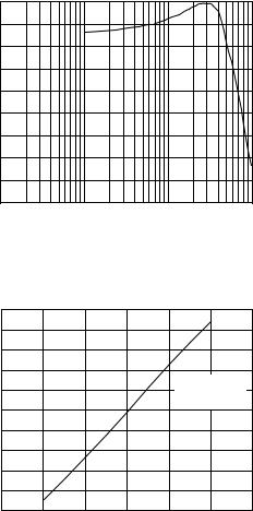
Figure 7. THD vs. Input Frequency
|
–70 |
|
|
|
|
–60 |
|
FIN = 1MHz |
|
|
–50 |
|
|
|
THD – dB |
–40 |
|
|
|
–30 |
|
|
|
|
|
–20 |
|
|
|
|
–10 |
|
|
|
|
0 |
|
10E+06 |
|
|
100E+03 |
1E+06 |
100E+06 |
CLOCK FREQUENCY – Hz
Figure 8. THD vs. Clock Frequency
|
1.005 |
|
|
|
|
|
|
|
|
1.004 |
|
|
|
|
|
|
|
|
1.003 |
|
|
|
|
|
|
|
V |
1.002 |
|
|
|
|
|
|
|
– |
|
|
|
|
|
|
|
|
REF |
1.001 |
|
|
|
|
|
|
|
V |
|
|
|
|
|
|
|
|
|
1.000 |
|
|
|
|
|
|
|
|
0.999 |
|
|
|
|
|
|
|
|
0.998 |
|
0 |
20 |
40 |
60 |
80 |
|
|
–40 |
–20 |
100 |
|||||
|
|
|
|
TEMPERATURE – °C |
|
|
|
|
Figure 10. Power Consumption vs. Clock Frequency (MODE = AVSS)
|
1M |
|
|
|
|
900k |
|
|
|
|
800k |
|
|
|
|
700k |
|
|
|
|
600k |
|
|
|
HITS |
500k |
|
499856 |
|
|
|
|
||
400k |
|
|
|
|
|
|
|
|
|
|
300k |
|
|
|
|
200k |
|
|
|
|
100k |
54383 |
|
54160 |
|
0 |
N–1 |
N |
N+1 |
|
|
|||
|
|
|
CODE |
|
Figure 11. Grounded Input Histogram
20
0
CLOCK = 20MHz
–20
–40
–60
–80
–100
–120
–140
0E+0 1E+6 2E+6 3E+6 4E+6 5E+6 6E+6 7E+6 8E+6 9E+6 10E+6 SINGLE TONE FREQUENCY DOMAIN
Figure 9. Voltage Reference Error vs. Temperature |
Figure 12. Single-Tone Frequency Domain |
REV. E |
–7– |
AD9200
|
0 |
|
|
–3 |
|
– dB |
–6 |
|
–9 |
||
AMPLITUDE |
||
–12 |
||
|
||
SIGNAL |
–15 |
|
–18 |
||
|
||
|
–21 |
–24
–27
1.0E+6 |
10.0E+6 |
100.0E+6 |
1.0E+9 |
FREQUENCY – Hz
Figure 13. Full Power Bandwidth
|
25 |
|
|
|
|
|
|
|
20 |
|
|
|
|
|
|
|
15 |
|
|
|
|
|
|
|
10 |
|
|
|
|
REFBS = 0.5V |
|
|
|
|
|
|
|
|
|
–mA |
5 |
|
|
|
|
REFTS = 2.5V |
|
0 |
|
|
|
|
CLOCK = 20MHz |
|
|
|
|
|
|
|
|
||
|
|
|
|
|
|
|
|
B |
|
|
|
|
|
|
|
I |
–5 |
|
|
|
|
|
|
|
|
|
|
|
|
|
|
|
–10 |
|
|
|
|
|
|
|
–15 |
|
|
|
|
|
|
|
–20 |
|
|
|
|
|
|
|
–25 |
0.5 |
1.0 |
1.5 |
2.0 |
2.5 |
3.0 |
|
0 |
||||||
INPUT VOLTAGE – V
APPLYING THE AD9200
THEORY OF OPERATION
The AD9200 implements a pipelined multistage architecture to achieve high sample rate with low power. The AD9200 distributes the conversion over several smaller A/D subblocks, refining the conversion with progressively higher accuracy as it passes the results from stage to stage. As a consequence of the distributed conversion, the AD9200 requires a small fraction of the 1023 comparators used in a traditional flash type A/D. A sample-and-hold function within each of the stages permits the first stage to operate on a new input sample while the second, third and fourth stages operate on the three preceding samples.
OPERATIONAL MODES
The AD9200 is designed to allow optimal performance in a wide variety of imaging, communications and instrumentation applications, including pin compatibility with the AD876 A/D. To realize this flexibility, internal switches on the AD9200 are used to reconfigure the circuit into different modes. These modes are selected by appropriate pin strapping. There are three parts of the circuit affected by this modality: the voltage reference, the reference buffer, and the analog input. The nature of the application will determine which mode is appropriate: the descriptions in the following sections, as well as the Table I should assist in picking the desired mode.
Figure 14. Input Bias Current vs. Input Voltage
Table I. Mode Selection
|
Input |
Input |
MODE |
REFSENSE |
|
|
|
|
|
Modes |
Connect |
Span |
Pin |
Pin |
REF |
REFTS |
|
REFBS |
Figure |
|
|
|
|
|
|
|
|
|
|
TOP/BOTTOM |
AIN |
1 V |
AVDD |
Short REFSENSE, REFTS and VREF Together |
|
AGND |
18 |
||
|
|
|
|
|
|
|
|
|
|
|
AIN |
2 V |
AVDD |
AGND |
Short REFTS and VREF Together |
|
AGND |
19 |
|
|
|
|
|
|
|
|
|
|
|
CENTER SPAN |
AIN |
1 V |
AVDD/2 |
Short VREF and REFSENSE Together |
AVDD/2 |
|
AVDD/2 |
20 |
|
|
|
|
|
|
|
|
|
|
|
|
AIN |
2 V |
AVDD/2 |
AGND |
No Connect |
AVDD/2 |
|
AVDD/2 |
|
|
|
|
|
|
|
|
|
|
|
Differential |
AIN Is Input 1 |
1 V |
AVDD/2 |
Short VREF and REFSENSE Together |
AVDD/2 |
|
AVDD/2 |
29 |
|
|
REFTS and |
|
|
|
|
|
|
|
|
|
|
|
|
|
|
|
|
|
|
|
REFBS Are |
|
|
|
|
|
|
|
|
|
Shorted Together |
|
|
|
|
|
|
|
|
|
for Input 2 |
2 V |
AVDD/2 |
AGND |
No Connect |
AVDD/2 |
|
AVDD/2 |
|
|
|
|
|
|
|
|
|
|
|
External Ref |
AIN |
2 V max |
AVDD |
AVDD |
No Connect |
Span = REFTS |
21, 22 |
||
|
|
|
|
|
|
– REFBS (2 V max) |
|
||
|
|
|
|
|
|
|
|||
|
|
|
|
|
|
|
|
|
|
|
|
|
AGND |
|
|
Short to |
|
Short to |
23 |
|
|
|
|
|
|
||||
|
|
|
|
|
|
VREFTF |
|
VREFBF |
|
|
|
|
|
|
|
|
|
|
|
AD876 |
AIN |
2 V |
Float or |
AVDD |
No Connect |
Short to |
|
Short to |
30 |
|
|
|
AVSS |
|
|
VREFTF |
|
VREFBF |
|
|
|
|
|
|
|
|
|
|
|
–8– |
REV. E |
Loading...