


 Loading...
Fast, Voltage-Out DC–440 MHz,
95 dB Logarithmic Amplifier
AD8310
FEATURES
Multistage demodulating logarithmic amplifier Voltage output, rise time <15 ns
High current capacity: 25 mA into grounded RL 95 dB dynamic range: −91 dBV to +4 dBV Single supply of 2.7 V min at 8 mA typ
DC–440 MHz operation, ±0.4 dB linearity Slope of +24 mV/dB, intercept of −108 dBV Highly stable scaling over temperature Fully differential dc-coupled signal path 100 ns power-up time, 1 mA sleep current
FUNCTIONAL BLOCK DIAGRAM
|
|
VPOS |
BAND GAP REFERENCE |
|
AD8310 |
ENBL |
|
ENABLE |
|||
SUPPLY |
5 |
8mA |
|
|
|
7 |
|||||
|
|
|
AND BIASING |
|
|
|
|
|
|
|
|
|
|
|
SIX 14.3dB 900MHz |
|
|
|
|
BFIN |
6 |
BUFFER |
|
|
|
INHI |
AMPLIFIER STAGES |
|
|
|
|
|
|||
+INPUT |
8 |
|
|
|
|
|
|
|
INPUT |
|
|
–INPUT |
1 |
1.0kΩ |
|
MIRROR |
|
|
|
|
|
||
INLO |
|
|
2µA |
|
+ |
VOUT |
|
|
|
||
|
|
3 |
|
|
|
4 |
OUTPUT |
||||
|
|
|
|
/dB |
|
– |
|||||
|
|
|
|
2 |
3kΩ |
|
|
|
|
|
|
|
|
NINE DETECTOR CELLS |
|
3kΩ |
|
|
|
||||
|
|
|
SPACED 14.3dB |
|
COMM |
1kΩ |
|
|
|
|
|
COMMON |
2 |
COMM |
|
|
|
|
|
|
|||
|
|
|
|
|
|
|
|
||||
|
|
|
COMM |
|
|
|
|
||||
|
|
|
INPUT-OFFSET |
|
|
OFLT |
3 |
OFFSET |
|
||
|
|
|
|
|
|
|
|
||||
|
|
COMPENSATION LOOP |
|
|
|
|
33pF |
|
FILTER |
001 |
|
|
|
|
|
|
|
|
COMM |
|
|
01084- |
|
|
|
|
|
|
|
|
|
|
|
|
|
APPLICATIONS
Conversion of signal level to decibel form
Transmitter antenna power measurement
Receiver signal strength indication (RSSI)
Low cost radar and sonar signal processing
Network and spectrum analyzers
Signal-level determination down to 20 Hz
True-decibel ac mode for multimeters
GENERAL DESCRIPTION
The AD8310 is a complete, dc–440 MHz demodulating logarithmic amplifier (log amp) with a very fast voltage mode output, capable of driving up to 25 mA into a grounded load in under 15 ns. It uses the progressive compression (successive detection) technique to provide a dynamic range of up to 95 dB to ±3 dB law conformance or 90 dB to a ±1 dB error bound up to 100 MHz. It is extremely stable and easy to use, requiring no significant external components. A single-supply voltage of
2.7 V to 5.5 V at 8 mA is needed, corresponding to a power consumption of only 24 mW at 3 V. A fast-acting CMOScompatible enable pin is provided.
Each of the six cascaded amplifier/limiter cells has a smallsignal gain of 14.3 dB, with a −3 dB bandwidth of 900 MHz. A total of nine detector cells are used to provide a dynamic range that extends from −91 dBV (where 0 dBV is defined as the amplitude of a 1 V rms sine wave), an amplitude of about ±40 µV, up to +4 dBV (or ±2.2 V). The demodulated output is accurately scaled, with a log slope of 24 mV/dB and an intercept of –108 dBV. The scaling parameters are supplyand temperature-independent.
Rev. D
Information furnished by Analog Devices is believed to be accurate and reliable. However, no responsibility is assumed by Analog Devices for its use, nor for any infringements of patents or other rights of third parties that may result from its use. Specifications subject to change without notice. No license is granted by implication or otherwise under any patent or patent rights of Analog Devices. Trademarks and registered trademarks are the property of their respective owners.
Figure 1.
The fully differential input offers a moderately high impedance (1 kΩ in parallel with about 1 pF). A simple network can match the input to 50 Ω and provide a power sensitivity of −78 dBm to +17 dBm. The logarithmic linearity is typically within ±0.4 dB up to 100 MHz over the central portion of the range, but it is somewhat greater at 440 MHz. There is no minimum frequency limit; the AD8310 can be used down to low audio frequencies. Special filtering features are provided to support this wide range.
The output voltage runs from a noise-limited lower boundary of 400 mV to an upper limit within 200 mV of the supply voltage for light loads. The slope and intercept can be readily altered using external resistors. The output is tolerant of a wide variety of load conditions and is stable with capacitive loads of 100 pF.
The AD8310 provides a unique combination of low cost, small size, low power consumption, high accuracy and stability, high dynamic range, a frequency range encompassing audio to UHF, fast response time, and good load-driving capabilities, making this product useful in numerous applications that require the reduction of a signal to its decibel equivalent.
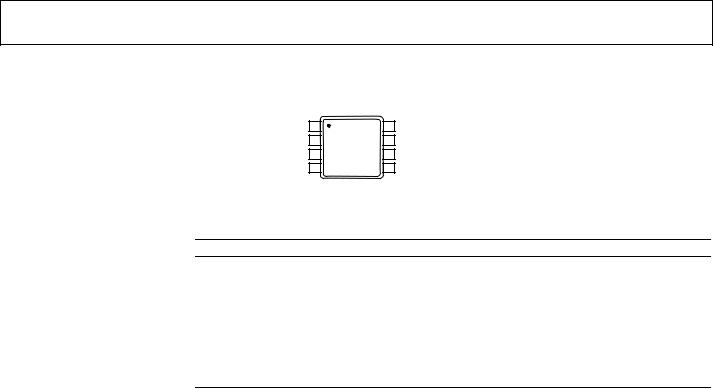
The AD8310 is available in the industrial temperature range of –40°C to +85°C in an 8-lead MSOP package.
One Technology Way, P.O. Box 9106, Norwood, MA 02062-9106, U.S.A. Tel: 781.329.4700 www.analog.com Fax: 781.326.8703 © 2004 Analog Devices, Inc. All rights reserved.

AD8310
TABLE OF CONTENTS |
|
Specifications..................................................................................... |
3 |
Absolute Maximum Ratings............................................................ |
4 |
ESD Caution.................................................................................. |
4 |
Pin Configuration and Function Descriptions............................. |
5 |
Typical Performance Characteristics ............................................. |
6 |
Theory of Operation ........................................................................ |
9 |
Progressive Compression ............................................................ |
9 |
Slope and Intercept Calibration................................................ |
10 |
Offset Control ............................................................................. |
10 |
Product Overview........................................................................... |
11 |
Enable Interface .......................................................................... |
11 |
Input Interface............................................................................. |
11 |
Offset Interface ........................................................................... |
12 |
Output Interface ......................................................................... |
12 |
Using the AD8310........................................................................... |
14 |
Basic Connections ...................................................................... |
14 |
Transfer Function in Terms of Slope and Intercept............... |
15 |
REVISION HISTORY |
|
10/04—Data Sheet Changed from Rev. C to Rev. D |
|
Format Updated .......................................................... |
Universal |
Typical Performance Characteristics Reordered ......................... |
6 |
Changes to Figures 41 and 42 ....................................................... |
20 |
7/03—Data Sheet Changed from Rev. B to Rev. C |
|
Replaced TPC 12............................................................................... |
5 |
Change to DC-Coupled Input Section ........................................ |
14 |
Replaced Figure 20 ......................................................................... |
15 |
Updated Outline Dimensions ....................................................... |
16 |
2/03—Data Sheet Changed from Rev. A to Rev. B |
|
Change to Evaluation Board Section ........................................... |
15 |
Change to Table III......................................................................... |
16 |
Updated Outline Dimensions ....................................................... |
16 |
1/00—Data Sheet Changed from Rev. 0 to Rev. A |
|
10/99—Revision 0: Initial Version |
|
dBV vs. dBm................................................................................ |
15 |
Input Matching ........................................................................... |
15 |
Narrow-Band Matching ............................................................ |
16 |
General Matching Procedure.................................................... |
16 |
Slope and Intercept Adjustments ............................................. |
17 |
Increasing the Slope to a Fixed Value ...................................... |
17 |
Output Filtering.......................................................................... |
18 |
Lowering the High-Pass Corner Frequency of the Offset |
|
Compensation Loop .................................................................. |
18 |
Applications..................................................................................... |
19 |
Cable-Driving ............................................................................. |
19 |
DC-Coupled Input ..................................................................... |
19 |
Evaluation Board ............................................................................ |
20 |
Outline Dimensions ....................................................................... |
22 |
Ordering Guide .......................................................................... |
22 |
Rev. D | Page 2 of 24
|
|
|
|
|
|
|
AD8310 |
||
|
|
|
|
|
|
|
|
|
|
|
SPECIFICATIONS |
|
|
|
|
|
|
|
|
|
TA = 25°C, VS = 5 V, unless otherwise noted. |
|
|
|
|
|
|
||
|
Table 1. |
|
|
|
|
|
|
|
|
|
Parameter |
Conditions |
Min |
Typ |
Max |
|
Unit |
||
|
|
|
|
|
|
|
|
|
|
|
INPUT STAGE |
Inputs INHI, INLO |
|
|
|
|
|
|
|
|
Maximum Input1 |
Single-ended, p-p |
±2.0 |
±2.2 |
|
|
V |
||
|
|
|
|
|
4 |
|
|
dBV |
|
|
Equivalent Power in 50 Ω |
Termination resistor of 52.3 Ω |
|
17 |
|
|
dBm |
||
|
|
Differential drive, p-p |
|
20 |
|
|
dBm |
||
|
Noise Floor |
Terminated 50 Ω source |
|
1.28 |
|
|
nV/√Hz |
||
|
Equivalent Power in 50 Ω |
440 MHz bandwidth |
|
−78 |
|
|
dBm |
||
|
Input Resistance |
From INHI to INLO |
800 |
1000 |
1200 |
|
Ω |
||
|
Input Capacitance |
From INHI to INLO |
|
1.4 |
|
|
pF |
||
|
DC Bias Voltage |
Either input |
|
3.2 |
|
|
V |
||
|
|
|
|
|
|
|
|
|
|
|
LOGARITHMIC AMPLIFIER |
Output VOUT |
|
|
|
|
|
|
|
|
±3 dB Error Dynamic Range |
From noise floor to maximum input |
|
95 |
|
|
dB |
||
|
Transfer Slope |
10 MHz ≤ f ≤ 200 MHz |
22 |
24 |
26 |
|
mV/dB |
||
|
|
Overtemperature, –40°C < TA < +85°C |
20 |
|
26 |
|
mV/dB |
||
|
Intercept (Log Offset)2 |
10 MHz ≤ f ≤ 200 MHz |
−115 |
−108 |
−99 |
|
dBV |
||
|
|
Equivalent dBm (re 50 Ω) |
−102 |
−95 |
−86 |
|
dBm |
||
|
|
Overtemperature, −40°C ≤ TA ≤ +85°C |
−120 |
|
−96 |
|
dBV |
||
|
|
Equivalent dBm (re 50 Ω) |
−107 |
|
−83 |
|
dBm |
||
|
|
Temperature sensitivity |
|
−0.04 |
|
|
dB/°C |
||
|
Linearity Error (Ripple) |
Input from –88 dBV (–75 dBm) to +2 dBV (+15 dBm) |
|
±0.4 |
|
|
dB |
||
|
Output Voltage |
Input = –91 dBV (–78 dBm) |
|
0.4 |
|
|
V |
||
|
|
Input = 9 dBV (22 dBm) |
|
2.6 |
|
|
V |
||
|
Minimum Load Resistance, RL |
|
|
|
100 |
|
|
Ω |
|
|
Maximum Sink Current |
|
|
|
0.5 |
|
|
mA |
|
|
Output Resistance |
|
|
|
0.05 |
|
|
Ω |
|
|
Video Bandwidth |
|
|
|
25 |
|
|
MHz |
|
|
Rise Time (10% to 90%) |
Input Level = −43 dBV (−30 dBm), RL ≥ 402 Ω, CL ≤ 68 pF |
|
15 |
|
|
ns |
||
|
|
Input Level = −3 dBV (+10 dBm), RL ≥ 402 Ω, CL ≤ 68 pF |
|
20 |
|
|
ns |
||
|
Fall Time (90% to 10%) |
Input Level = −43 dBV (−30 dBm), RL ≥ 402 Ω, CL ≤ 68 pF |
|
30 |
|
|
ns |
||
|
|
Input Level = −3 dBV (+10 dBm), RL ≥ 402 Ω, CL ≤ 68 pF |
|
40 |
|
|
ns |
||
|
Output Settling Time to 1% |
Input Level = −13 dBV (0 dBm), RL ≥ 402 Ω, CL ≤ 68 pF |
|
40 |
|
|
ns |
||
|
POWER INTERFACES |
|
|
|
|
|
|
|
|
|
Supply Voltage, VPOS |
|
|
2.7 |
|
5.5 |
|
V |
|
|
Quiescent Current |
Zero-signal |
6.5 |
8.0 |
9.5 |
|
mA |
||
|
Overtemperature |
−40°C < TA< +85°C |
5.5 |
8.5 |
10 |
|
mA |
||
|
Disable Current |
|
|
|
0.05 |
|
|
µA |
|
|
Logic Level to Enable Power |
High condition, −40°C < TA< +85°C |
|
2.3 |
|
|
V |
||
|
Input Current when High |
3 V at ENBL |
|
35 |
|
|
µA |
||
|
Logic Level to Disable Power |
Low condition, −40°C < TA< +85°C |
|
0.8 |
|
|
V |
||
|
|
|
|
|
|
|
|
|
|
|
|
|
|
|
|
|
|
|
|
1The input level is specified in dBV, because logarithmic amplifiers respond strictly to voltage, not power. 0 dBV corresponds to a sinusoidal single-frequency input of 1 V rms. A power level of 0 dBm (1 mW) in a 50 Ω termination corresponds to an input of 0.2236 V rms. Therefore, the relationship between dBV and dBm is a fixed offset of 13 dBm in the special case of a 50 Ω termination.
2 Guaranteed but not tested; limits are specified at six sigma levels.
Rev. D | Page 3 of 24

AD8310
ABSOLUTE MAXIMUM RATINGS
Table 2.
Parameter |
Value |
|
|
Supply Voltage, VS |
7.5 V |
Input Power (re 50 Ω), Single-Ended |
18 dBm |
Differential Drive |
22 dBm |
Internal Power Dissipation |
200 mW |
θJA |
200°C/W |
Maximum Junction Temperature |
125°C |
Operating Temperature Range |
−40°C to +85°C |
Storage Temperature Range |
–65°C to +150°C |
Lead Temperature Range (Soldering 60 s) |
300°C |
|
|
Stresses above those listed under Absolute Maximum Ratings may cause permanent damage to the device. This is a stress rating only; functional operation of the device at these or any other conditions above those indicated in the operational section of this specification is not implied. Exposure to absolute maximum rating conditions for extended periods may effect device reliability.
ESD CAUTION
ESD (electrostatic discharge) sensitive device. Electrostatic charges as high as 4000 V readily accumulate on the human body and test equipment and can discharge without detection. Although this product features proprietary ESD protection circuitry, permanent damage may occur on devices subjected to high energy electrostatic discharges. Therefore, proper ESD precautions are recommended to avoid performance degradation or loss of functionality.
Rev. D | Page 4 of 24
AD8310
PIN CONFIGURATION AND FUNCTION DESCRIPTIONS
INLO |
1 |
AD8310 |
|
COMM |
2 |
||
OFLT |
3 |
TOP VIEW |
|
(Not to Scale) |
|||
VOUT |
|
||
4 |
|
8 INHI
7 ENBL
6 BFIN
5 VPOS
01084-002
|
|
Figure 2. Pin Configuration |
Table 3. Pin Function Descriptions |
|
|
Pin No. |
Mnemonic |
Function |
|
|
|
1 |
INLO |
One of Two Balanced Inputs, Biased Roughly to VPOS/2. |
2 |
COMM |
Common Pin (Usually Grounded). |
3 |
OFLT |
Offset Filter Access, Nominally at about 1.75 V. |
4 |
VOUT |
Low Impedance Output Voltage, 25 mA Maximum Load. |
5 |
VPOS |
Positive Supply, 2.7 V to 5.5 V at 8 mA Quiescent Current. |
6 |
BFIN |
Buffer Input; Used to Lower Postdetection Bandwidth. |
7 |
ENBL |
CMOS Compatible Chip Enable (Active when High). |
8 |
INHI |
Second of Two Balanced Inputs. |
Rev. D | Page 5 of 24
AD8310
TYPICAL PERFORMANCE CHARACTERISTICS
|
3.0 |
|
|
|
|
|
|
|
|
2.5 |
|
|
|
|
|
|
|
(V) |
2.0 |
|
|
|
|
|
|
|
|
|
|
|
|
|
|
|
|
RSSI OUTPUT |
1.5 |
|
|
|
|
|
|
|
1.0 |
TA = –40°C |
|
|
|
|
|
|
|
|
TA = +25°C |
|
|
|
|
|
|
|
|
0.5 |
|
|
|
|
|
|
01084-011 |
|
|
TA = +85°C |
|
|
|
|||
|
0 |
|
|
|
|
|
|
|
|
|
–80 |
–60 |
–40 |
–20 |
0 |
|
|
|
–120 |
–100 |
20 |
|||||
|
|
(–87dBm) |
|
INPUT LEVEL (dBV) |
|
(+13dBm) |
|
|
|
|
|
|
|
|
|
||
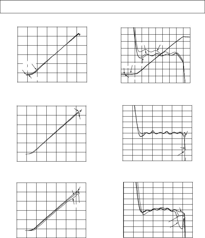
Figure 3. RSSI Output vs. Input Level, 100 MHz Sine Input at TA = −40°C, +25°C, and +85°C, Single-Ended Input
|
3.0 |
|
|
|
|
10MHz |
|
50MHz |
|
|
|
|
|
|
|
|
|
||
|
2.5 |
|
|
|
|
|
|
|
|
|
|
|
|
|
|
|
100MHz |
|
|
(V) |
2.0 |
|
|
|
|
|
|
|
|
|
|
|
|
|
|
|
|
|
|
RSSI OUTPUT |
1.5 |
|
|
|
|
|
|
|
|
1.0 |
|
|
|
|
|
|
|
|
|
|
|
|
|
|
|
|
|
|
|
|
0.5 |
|
|
|
|
|
|
|
|
|
0 |
–100 |
–80 |
–60 |
–40 |
–20 |
0 |
20 |
01084-012 |
|
–120 |
||||||||
|
|
(–87dBm) |
|
INPUT LEVEL (dBV) |
(+13dBm) |
||||
|
|
|
|
|
|
|
|||
Figure 4. RSSI Output vs. Input Level at TA = 25°C for Frequencies of 10 MHz, 50 MHz, and 100 MHz
|
3.0 |
|
|
|
|
|
200MHz |
|
|
|
|
|
|
|
|
||
|
|
|
|
|
|
300MHz |
|
|
|
2.5 |
|
|
|
|
|
|
|
(V) |
2.0 |
|
|
|
|
|
|
|
|
|
|
|
|
|
|
|
|
OUTPUTRSSI |
|
|
|
|
|
|
440MHz |
|
|
|
|
|
|
|
|
|
|
|
1.5 |
|
|
|
|
|
|
|
|
1.0 |
|
|
|
|
|
|
|
|
0.5 |
|
|
|
|
|
|
|
|
0 |
|
|
|
|
|
|
|
|
–120 |
–100 |
–80 |
–60 |
–40 |
–20 |
0 |
20 |
|
|
(–87dBm) |
|
INPUT LEVEL (dBV) |
|
(+13dBm) |
01084013- |
|
Figure 5. RSSI Output vs. Input Level at TA = 25°C for Frequencies of 200 MHz, 300 MHz, and 440 MHz
|
2.4 |
|
|
|
|
|
|
|
|
|
|
4.0 |
|
|
2.1 |
|
|
|
|
|
|
|
|
|
|
3.0 |
|
|
1.8 |
|
|
|
+25°C |
|
–40°C |
|
|
|
2.0 |
|
|
|
|
|
|
|
|
|
|
|
|
|
|||
(V) |
1.5 |
|
|
|
|
|
|
|
|
|
|
1.0 |
(dB) |
|
|
|
|
|
|
|
|
|
|
|
|
||
V |
1.2 |
|
|
|
|
|
|
|
|
|
|
0 |
ERROR |
OUT |
|
|
|
|
|
|
|
|
|
|
|
|
|
|
0.9 |
|
–40°C |
+85°C |
|
|
|
|
|
|
–1.0 |
|
|
|
|
|
|
|
|
|
|
|
|
|
|||
|
0.6 |
+85°C |
|
|
|
|
|
|
|
|
–2.0 |
|
|
|
0.3 |
|
+25°C |
|
|
|
|
|
|
|
–3.0 |
|
|
|
|
|
|
|
|
|
|
|
|
|
|
||
|
0 |
|
|
|
|
PIN (dBm) |
|
|
|
–4.0 |
014-01084 |
||
|
–90 |
–80 |
–70 |
–60 |
–50 |
–40 |
–30 |
–20 |
–10 |
0 |
10 |
|
|
Figure 6. Log Linearity of RSSI Output vs. Input Level, 100 MHz Sine Input at TA = −40°C, +25°C, and +85°C
|
5 |
|
|
|
|
|
|
|
|
|
4 |
|
|
|
|
|
|
|
|
|
3 |
|
|
|
|
|
|
|
|
|
2 |
|
|
|
|
|
|
|
|
(dB) |
1 |
|
|
|
|
|
|
10MHz |
|
|
|
|
|
|
|
|
|
||
ERROR |
0 |
|
|
|
|
|
|
|
|
–1 |
|
|
|
|
|
|
|
|
|
|
–2 |
|
|
|
|
50MHz |
|
|
|
|
–3 |
|
|
|
|
|
|
|
|
|
|
|
|
|
|
|
|
|
|
|
–4 |
|
|
|
|
100MHz |
|
|
|
|
|
|
|
|
|
|
|
|
|
|
–5 |
–100 |
–80 |
–60 |
–40 |
–20 |
0 |
20 |
01084-015 |
|
–120 |
||||||||
|
|
(–87dBm) |
|
INPUT LEVEL (dBV) |
(+13dBm) |
||||
|
|
|
|
|
|
|
|||
Figure 7. Log Linearity of RSSI Output vs. Input Level, at TA = 25°C, for Frequencies of 10 MHz, 50 MHz, and 100 MHz
|
5 |
|
|
|
|
|
|
|
|
4 |
|
|
|
|
|
|
|
|
3 |
|
|
|
|
|
|
|
(dB) |
2 |
|
|
|
|
|
|
|
1 |
|
|
|
|
200MHz |
|
||
ERROR |
–1 |
|
|
|
|
|
|
|
|
0 |
|
|
|
|
|
|
|
|
–2 |
|
|
|
300MHz |
|
|
|
|
–3 |
|
|
|
|
|
||
|
|
|
|
440MHz |
|
|
||
|
|
|
|
|
|
|
||
|
–4 |
|
|
|
|
|
|
|
|
–5 |
–100 |
–80 |
–60 |
–40 |
–20 |
0 |
20 |
|
–120 |
|||||||
|
|
(–87dBm) |
|
INPUT LEVEL (dBV) |
|
(+13dBm) |
01084016- |
|
|
|
|
|
|
||||
|
|
|
|
|
|
|
||
Figure 8. Log Linearity of RSSI Output vs. Input Level at TA = 25°C for Frequencies of 200 MHz, 300 MHz, and 440 MHz
Rev. D | Page 6 of 24

AD8310
100pF |
|
500mV PER |
VOUT |
VERTICAL |
|
|
DIVISION |
|
3300pF |
|
|
|
|
|
|
0.01µF |
|
|
GROUND REFERENCE |
|
50µs PER |
|
|
HORIZONTAL |
01084-009 |
|
DIVISION |
|
|
|
|
|
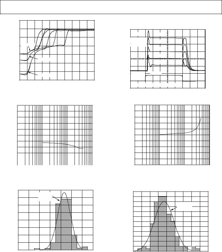
Figure 9. Small-Signal AC Response of RSSI Output with External BFIN Capacitance of 100 pF, 3300 pF, and 0.01 µF
VOUT |
|
200Ω |
|
|
|
500mV PER |
100Ω |
154Ω |
|
|
|
VERTICAL |
|
|
DIVISION |
|
|
GND REFERENCE |
|
|
INPUT |
|
|
500mV PER |
|
100ns PER |
VERTICAL |
|
HORIZONTAL |
DIVISION |
|
DIVISION |
|
01084-005 |
Figure 10. Large-Signal RSSI Pulse Response with CL = 100 pF |
|
and RL = 100 Ω, 154 Ω, and 200 Ω |
|
VOUT |
100ns PER |
HORIZONTAL |
|
500mV PER |
DIVISION |
|
|
VERTICAL |
|
DIVISION |
|
GND REFERENCE |
|
INPUT |
|
–3dBV INPUT |
500mV PER |
LEVEL SHOWN |
VERTICAL |
HERE |
DIVISION |
|
01084006- |
Figure 11. RSSI Pulse Response with RL = 402 Ω and CL = 68 pF, for Inputs Stepped from 0 dBV to −33 dBV, −23 dBV, −13 dBV, and −3 dBV
500mV PER |
VOUT |
VERTICAL |
|
DIVISION |
25ns PER |
|
|
|
HORIZONTAL |
|
DIVISION |
GROUND REFERENCE
10mV PER VERTICAL DIVISION
INPUT
01084-010
Figure 12. Small-Signal RSSI Pulse Response with RL = 402 Ω and CL = 68 pF
VOUT |
CURVES |
500mV PER |
OVERLAP |
VERTICAL |
|
DIVISION |
|
GND REFERENCE
INPUT |
|
500mV PER |
100ns PER |
VERTICAL |
HORIZONTAL |
DIVISION |
DIVISION |
|
01084007- |
Figure 13. Large-Signal RSSI Pulse Response with RL = 100 Ω |
|
and CL = 33 pF, 68 pF, and 100 pF |
|
VOUT |
|
200mV PER |
100ns PER |
HORIZONTAL |
|
VERTICAL |
DIVISION |
DIVISION |
|
GND REFERENCE |
|
INPUT |
|
|
20mV PER |
|
VERTICAL |
|
DIVISION |
|
01084008- |
Figure 14. Small-Signal RSSI Pulse Response with RL = 50 Ω and Back Termination of 50 Ω (Total Load = 100 Ω)
Rev. D | Page 7 of 24
AD8310 |
|
|
|
|
|
|
|
|
|
|
|
|
|
100 |
|
|
|
|
|
|
|
|
|
|
|
|
10 |
|
|
|
|
|
|
|
|
|
|
|
(mA) |
1 |
|
|
|
|
|
|
|
|
|
|
|
|
|
|
|
|
|
|
|
|
|
|
|
|
CURRENT |
0.1 |
TA = +85°C |
|
|
|
|
|
|
|
|
|
|
0.01 |
|
|
|
|
|
|
|
|
|
|
|
|
SUPPLY |
|
|
|
|
|
|
|
|
|
|
|
|
|
|
|
TA = +25°C |
|
|
|
|
|
|
|
||
0.001 |
|
|
|
|
|
|
|
|
|
|
|
|
|
0.0001 |
|
|
TA = –40°C |
|
|
|
|
|
|
|
|
|
|
|
|
|
|
|
|
|
|
|
||
0.00001 |
|
|
|
|
|
|
|
|
|
|
01084-003 |
|
|
0.5 |
0.7 |
0.9 |
1.1 |
1.3 |
1.5 |
1.7 |
1.9 |
2.1 |
2.3 |
2.5 |
|
|
|
|
|
ENABLE VOLTAGE (V) |
|
|
|
|||||
|
|
|
|
|
|
|
|
|||||
Figure 15. Supply Current vs. Enable Voltage at TA = −40°C, +25°C, and +85°C
|
30 |
|
|
29 |
|
|
28 |
|
(mV/dB) |
27 |
|
26 |
||
SLOPE |
||
25 |
||
|
||
RSSI |
24 |
|
23 |
||
|
22
21 |
|
|
|
|
|
|
|
|
|
|
|
20 |
|
|
|
|
|
|
|
|
017-01084 |
||
1 |
10 |
100 |
1000 |
||
FREQUENCY (MHz)
Figure 16. RSSI Slope vs. Frequency
|
40 |
|
NORMAL |
|
|
|
|
|
|
|
|
|
|
|
|
||
|
35 |
|
(23.6584, |
|
|
|
|
|
|
|
0.308728) |
|
|
|
|
||
|
|
|
|
|
|
|
||
|
30 |
|
|
|
|
|
|
|
|
25 |
|
|
|
|
|
|
|
COUNT |
20 |
|
|
|
|
|
|
|
|
|
|
|
|
|
|
|
|
|
15 |
|
|
|
|
|
|
|
|
10 |
|
|
|
|
|
|
|
|
5 |
|
|
|
|
|
|
|
|
0 |
22.0 |
22.5 |
23.0 |
23.5 |
24.0 |
24.5 |
01084-019 |
|
21.5 |
|||||||
|
|
|
|
SLOPE (mV/dB) |
|
|
||
Figure 17. Transfer Slope Distribution, VS = 5 V, Frequency = 100 MHz, 25°C |
||||||||
VOUT |
–3dBV |
|
|
500mV PER |
–23dBV |
|
|
VERTICAL |
|
||
|
|
||
DIVISION |
–43dBV |
|
|
|
|
||
|
–63dBV |
|
|
|
–83dBV |
|
|
5V PER |
ENABLE |
|
|
VERTICAL |
|
|
|
DIVISION |
|
01084-004 |
|
200ns PER HORIZONTAL DIVISION |
|||
|
|||
Figure 18. Power-On/Off Response Time with RF Input of −83 dBV to −3 dBV
|
–99 |
|
|
|
|
|
–101 |
|
|
|
|
(dBV) |
–103 |
|
|
|
|
–105 |
|
|
|
|
|
|
|
|
|
|
|
INTERCEPT |
–107 |
|
|
|
|
–111 |
|
|
|
|
|
|
–109 |
|
|
|
|
RSSI |
–113 |
|
|
|
|
|
–115 |
|
|
|
|
|
–117 |
|
|
|
|
|
–119 |
|
|
|
01084-018 |
|
1 |
10 |
100 |
1000 |
|
|
|
FREQUENCY (MHz) |
|
||
Figure 19. RSSI Intercept vs. Frequency
|
24 |
|
|
|
|
|
|
|
|
|
|
|
22 |
|
|
|
|
|
|
|
|
|
|
|
20 |
|
|
|
|
|
NORMAL |
|
|
|
|
|
|
|
|
|
|
|
|
|
|
||
|
18 |
|
|
|
|
|
(–107.6338, |
|
|
|
|
|
16 |
|
|
|
|
|
2.36064) |
|
|
|
|
|
|
|
|
|
|
|
|
|
|
|
|
COUNT |
14 |
|
|
|
|
|
|
|
|
|
|
12 |
|
|
|
|
|
|
|
|
|
|
|
10 |
|
|
|
|
|
|
|
|
|
|
|
|
|
|
|
|
|
|
|
|
|
|
|
|
8 |
|
|
|
|
|
|
|
|
|
|
|
6 |
|
|
|
|
|
|
|
|
|
|
|
4 |
|
|
|
|
|
|
|
|
|
|
|
2 |
|
|
|
|
|
|
|
|
|
|
|
0 |
–113 |
–111 |
–109 |
–107 |
–105 |
–103 |
–101 |
–99 |
–97 |
01084-020 |
|
–115 |
||||||||||
|
|
|
|
INTERCEPT (dBV) |
|
|
|
||||
Figure 20. Intercept Distribution VS = 5 V, Frequency = 100 MHz, 25°C |
|||||||||||
Rev. D | Page 8 of 24
Loading...