


Analog Devices AD8534ARU, AD8534AR, AD8534AN, AD8532ARU, AD8532ARM Datasheet
...a |
Low Cost, 250 mA Output |
|
Single-Supply Amplifiers |
||
|
|
AD8531/AD8532/AD8534 |
FEATURES
Single-Supply Operation: 2.7 Volts to 6 Volts High Output Current: 250 mA
Low Supply Current: 750 A/Amplifier
Wide Bandwidth: 3 MHz Slew Rate: 5 V/ s
No Phase Reversal
Low Input Currents
Unity Gain Stable Rail-to-Rail Input and Output
APPLICATIONS
Multimedia Audio
LCD Driver
ASIC Input or Output Amplifier
Headphone Driver
GENERAL DESCRIPTION
The AD8531, AD8532, and AD8534 are single, dual and quad rail-to-rail input and output single-supply amplifiers featuring 250 mA output drive current. This high output current makes these amplifiers excellent for driving either resistive or capacitive loads. AC performance is very good with 3 MHz bandwidth, 5 V/ s slew rate and low distortion. All are guaranteed to operate from a 3 volt single supply as well as a 5 volt supply.
The very low input bias currents enable the AD853x to be used for integrators, diode amplification and other applications requiring low input bias current. Supply current is only 750 A per amplifier at 5 volts, allowing low current applications to control high current loads.
Applications include audio amplification for computers, sound ports, sound cards and set-top boxes. The AD853x family is very stable and capable of driving heavy capacitive loads, such as those found in LCDs.
The ability to swing rail-to-rail at the inputs and outputs enables designers to buffer CMOS DACs, ASICs or other wide output swing devices in single-supply systems.
The AD8531, AD8532, and AD8534 are specified over the extended industrial (–40°C to +85°C) temperature range. The AD8531. The AD8532 is available in 8-lead plastic DIP, SOIC, MSOP, TSSOP surface-mount packages. The AD8534 is available in 14-lead plastic DIP, narrow SO-14 and 14-lead TSSOP surface-mount packages. All TSSOP, SOT, and SC70 versions are available in tape and reel only.
PIN CONFIGURATIONS
5-Lead SC70 and SOT-23
(KS and RT Suffixes)
OUT A |
1 |
AD8531 |
V+ |
5 |
|||
V 2 |
|
|
|
+IN A |
3 |
4 |
IN A |
8-Lead DIP, SOIC, TSSOP, and MSOP
(N, R, RU, and RM Suffixes)
NULL |
1 |
AD8531 |
8 |
NC |
–IN A |
2 |
|
7 |
V+ |
+IN A |
3 |
|
6 |
OUT A |
V– |
4 |
|
5 |
NULL |
8-Lead DIP, SOIC, TSSOP, and MSOP
(N, R, RU, and RM Suffixes)
OUT A |
1 |
AD8532 |
8 |
V+ |
–IN A |
2 |
|
7 |
OUT B |
+IN A |
3 |
|
6 |
–IN B |
V– |
4 |
|
5 |
+IN B |
14-Lead DIP, SOIC, and TSSOP
(N, R, and RU Suffixes)
OUT A |
1 |
14 |
OUT D |
–IN A |
2 |
13 |
–IN D |
+IN A |
3 |
12 |
+IN D |
V+ |
4 |
AD8534 |
V– |
11 |
|||
+IN B |
5 |
10 |
+IN C |
–IN B |
6 |
9 |
–IN C |
OUT B |
7 |
8 |
OUT C |
REV. C
Information furnished by Analog Devices is believed to be accurate and reliable. However, no responsibility is assumed by Analog Devices for its use, nor for any infringements of patents or other rights of third parties which may result from its use. No license is granted by implication or otherwise under any patent or patent rights of Analog Devices.
One Technology Way, P.O. Box 9106, Norwood, MA 02062-9106, U.S.A.
Tel: 781/329-4700 |
World Wide Web Site: http://www.analog.com |
Fax: 781/326-8703 |
© Analog Devices, Inc., 2000 |
AD8531/AD8532/AD8534–SPECIFICATIONS
ELECTRICAL CHARACTERISTICS (@ VS = 3.0 V, VCM = 1.5 V, TA = 25 C unless otherwise noted)
Parameter |
Symbol |
Conditions |
Min |
Typ |
Max |
Unit |
|
|
|
|
|
|
|
INPUT CHARACTERISTICS |
|
|
|
|
|
|
Offset Voltage |
VOS |
–40°C ≤ TA ≤ +85°C |
|
|
25 |
mV |
|
|
|
|
30 |
mV |
|
Input Bias Current |
IB |
–40°C ≤ TA ≤ +85°C |
|
5 |
50 |
pA |
Input Offset Current |
IOS |
|
|
60 |
pA |
|
–40°C ≤ TA ≤ +85°C |
|
1 |
25 |
pA |
||
|
|
|
|
30 |
pA |
|
Input Voltage Range |
|
|
0 |
|
3 |
V |
Common-Mode Rejection Ratio |
CMRR |
VCM = 0 V to 3 V |
38 |
45 |
|
dB |
Large Signal Voltage Gain |
AVO |
RL = 2 kΩ, VO = 0.5 V to 2.5 V |
|
25 |
|
V/mV |
Offset Voltage Drift |
∆VOS/∆T |
|
|
20 |
|
µV/°C |
Bias Current Drift |
∆IB/∆T |
|
|
50 |
|
fA/°C |
Offset Current Drift |
∆IOS/∆T |
|
|
20 |
|
fA/°C |
OUTPUT CHARACTERISTICS |
|
|
|
|
|
|
Output Voltage High |
VOH |
IL = 10 mA |
2.85 |
2.92 |
|
V |
Output Voltage Low |
VOL |
–40°C ≤ TA ≤ +85°C |
2.8 |
|
|
V |
IL = 10 mA |
|
60 |
100 |
mV |
||
Output Current |
IOUT |
–40°C ≤ TA ≤ +85°C |
|
±250 |
125 |
mV |
|
|
|
mA |
|||
Closed-Loop Output Impedance |
ZOUT |
f = 1 MHz, AV = 1 |
|
60 |
|
Ω |
POWER SUPPLY |
|
VS = 3 V to 6 V |
45 |
55 |
|
dB |
Power Supply Rejection Ratio |
PSRR |
|
||||
Supply Current/Amplifier |
ISY |
VO = 0 V |
|
0.70 |
1 |
mA |
|
|
–40°C ≤ TA ≤ +85°C |
|
|
1.25 |
mA |
DYNAMIC PERFORMANCE |
|
RL = 2 kΩ |
|
|
|
V/µs |
Slew Rate |
SR |
|
3.5 |
|
||
Settling Time |
tS |
To 0.01% |
|
1.6 |
|
µs |
Gain Bandwidth Product |
GBP |
|
|
2.2 |
|
MHz |
Phase Margin |
φo |
f = 1 kHz, RL = 2 kΩ |
|
70 |
|
Degrees |
Channel Separation |
CS |
|
65 |
|
dB |
|
|
|
|
|
|
|
|
NOISE PERFORMANCE |
|
|
|
|
|
nV/√Hz |
Voltage Noise Density |
en |
f = 1 kHz |
|
45 |
|
|
|
|
f = 10 kHz |
|
30 |
|
nV/√Hz |
Current Noise Density |
in |
f = 1 kHz |
|
0.05 |
|
pA/√Hz |
Specifications subject to change without notice.
–2– |
REV. C |
AD8531/AD8532/AD8534
ELECTRICAL CHARACTERISTICS (@ VS = 5.0 V, VCM = 2.5 V, TA = 25 C unless otherwise noted)
Parameter |
Symbol |
Conditions |
Min |
Typ |
Max |
Unit |
|
|
|
|
|
|
|
INPUT CHARACTERISTICS |
|
|
|
|
|
|
Offset Voltage |
VOS |
–40°C ≤ TA ≤ +85°C |
|
|
25 |
mV |
|
|
|
|
30 |
mV |
|
Input Bias Current |
IB |
–40°C ≤ TA ≤ +85°C |
|
5 |
50 |
pA |
Input Offset Current |
IOS |
|
|
60 |
pA |
|
–40°C ≤ TA ≤ +85°C |
|
1 |
25 |
pA |
||
|
|
|
|
30 |
pA |
|
Input Voltage Range |
|
|
0 |
|
5 |
V |
Common-Mode Rejection Ratio |
CMRR |
VCM = 0 V to 5 V |
38 |
47 |
|
dB |
Large Signal Voltage Gain |
AVO |
RL = 2 kΩ, VO = 0.5 V to 4.5 V |
15 |
80 |
|
V/mV |
Offset Voltage Drift |
∆VOS/∆T |
–40°C ≤ TA ≤ +85°C |
|
20 |
|
µV/°C |
Bias Current Drift |
∆IB/∆T |
|
|
50 |
|
fA/°C |
Offset Current Drift |
∆IOS/∆T |
|
|
20 |
|
fA/°C |
OUTPUT CHARACTERISTICS |
|
|
|
|
|
|
Output Voltage High |
VOH |
IL = 10 mA |
4.9 |
4.94 |
|
V |
Output Voltage Low |
VOL |
–40°C ≤ TA ≤ +85°C |
4.85 |
|
|
V |
IL = 10 mA |
|
50 |
100 |
mV |
||
Output Current |
IOUT |
–40°C ≤ TA ≤ +85°C |
|
±250 |
125 |
mV |
|
|
|
mA |
|||
Closed-Loop Output Impedance |
ZOUT |
f = 1 MHz, AV = 1 |
|
40 |
|
Ω |
POWER SUPPLY |
|
VS = 3 V to 6 V |
45 |
55 |
|
dB |
Power Supply Rejection Ratio |
PSRR |
|
||||
Supply Current/Amplifier |
ISY |
VO = 0 V |
|
0.75 |
1.25 |
mA |
|
|
–40°C ≤ TA ≤ +85°C |
|
|
1.75 |
mA |
DYNAMIC PERFORMANCE |
|
RL = 2 kΩ |
|
|
|
V/µs |
Slew Rate |
SR |
|
5 |
|
||
Full-Power Bandwidth |
BWp |
1% Distortion |
|
350 |
|
kHz |
Settling Time |
tS |
To 0.01% |
|
1.4 |
|
µs |
Gain Bandwidth Product |
GBP |
|
|
3 |
|
MHz |
Phase Margin |
φo |
f = 1 kHz, RL = 2 kΩ |
|
70 |
|
Degrees |
Channel Separation |
CS |
|
65 |
|
dB |
|
NOISE PERFORMANCE |
|
|
|
|
|
nV/√Hz |
Voltage Noise Density |
en |
f = 1 kHz |
|
45 |
|
|
|
|
f = 10 kHz |
|
30 |
|
nV/√Hz |
Current Noise Density |
in |
f = 1 kHz |
|
0.05 |
|
pA/√Hz |
Specifications subject to change without notice.
REV. C |
–3– |
AD8531/AD8532/AD8534
ABSOLUTE MAXIMUM RATINGS1 |
|
Supply Voltage (VS) . . . . . . . . . . . . . . . . . . . . |
. . . . . . . . . . 7 V |
Input Voltage . . . . . . . . . . . . . . . . . . . . . . . . . |
. . . . GND to VS |
Differential Input Voltage2 . . . . . . . . . . . . . . |
. . . . . . . . . ± 6 V |
Storage Temperature Range . . . . . . . . . . . . |
–65°C to +150°C |
Operating Temperature Range . . . . . . . . . . . |
–40°C to +85°C |
Junction Temperature Range . . . . . . . . . . . . |
–65°C to +150°C |
Lead Temperature Range (Soldering, 60 sec) |
. . . . . . . . 300°C |
NOTES
1Stresses above those listed under Absolute Maximum Ratings may cause permanent damage to the device. This is a stress rating only; the functional operation of the device at these or any other conditions above those indicated in the operational sections of this specification is not implied. Exposure to absolute maximum rating conditions for extended periods may affect device reliability.
2For supplies less than +6 volts, the differential input voltage is equal to ± VS.
PACKAGE INFORMATION
Package Type |
JA* |
JC |
Unit |
5-Lead SC70 (KS) |
376 |
126 |
°C/W |
5-Lead SOT-23 (RT) |
230 |
146 |
°C/W |
8-Lead SOIC (R) |
158 |
43 |
°C/W |
8-Lead MSOP (RM) |
210 |
45 |
°C/W |
8-Lead TSSOP (RU) |
240 |
43 |
°C/W |
8-Lead Plastic DIP (N) |
103 |
43 |
°C/W |
14-Lead Plastic DIP (N) |
83 |
39 |
°C/W |
14-Lead SOIC (R) |
120 |
36 |
°C/W |
14-Lead TSSOP (RU) |
240 |
43 |
°C/W |
*θJA is specified for the worst case conditions, i.e., θJA is specified for device in socket for P-DIP packages; θJA is specified for device soldered onto a circuit board for surface-mount packages.
ORDERING GUIDE
Model |
Temperature Range |
Package Description |
Package Option |
Branding Information |
|
|
|
|
|
AD8531AKS* |
–40°C to +85°C |
5-Lead SC70 |
KS-5 |
A7B |
AD8531AR |
–40°C to +85°C |
8-Lead SOIC |
SO-8 |
|
AD8531ART* |
–40°C to +85°C |
5-Lead SOT-23 |
RT-5 |
A7A |
AD8532AR |
–40°C to +85°C |
8-Lead SOIC |
SO-8 |
|
AD8532ARM* |
–40°C to +85°C |
8-Lead MSOP |
RM-8 |
ARA |
AD8532AN |
–40°C to +85°C |
8-Lead Plastic DIP |
N-8 |
|
AD8532ARU* |
–40°C to +85°C |
8-Lead TSSOP |
RU-8 |
|
AD8534AR |
–40°C to +85°C |
14-Lead SOIC |
SO-14 |
|
AD8534AN |
–40°C to +85°C |
14-Lead Plastic DIP |
N-14 |
|
AD8534ARU* |
–40°C to +85°C |
14-Lead TSSOP |
RU-14 |
|
*Available in reels only.
CAUTION
ESD (electrostatic discharge) sensitive device. Electrostatic charges as high as 4000 V readily accumulate on the human body and test equipment and can discharge without detection. Although the AD8531/AD8532/AD8534 features proprietary ESD protection circuitry, permanent damage may occur on devices subjected to high-energy electrostatic discharges. Therefore, proper ESD precautions are recommended to avoid performance degradation or loss of functionality.
2.5 |
|
|
|
|
|
|
|
|
|
|
|
–VOL |
|
|
|
|
|
|
|
|
|
2 |
+VOH |
|
|
|
|
|
|
|
|
|
|
|
|
|
|
|
|
|
|
||
1.5 |
|
|
|
|
|
|
|
|
|
|
OUT |
|
|
|
|
|
|
|
|
|
|
V |
|
|
|
|
|
|
|
|
|
|
1 |
|
|
|
|
|
|
|
|
|
|
0.5 |
|
|
|
|
|
|
|
|
|
|
0 |
20 |
40 |
60 |
80 |
100 |
120 |
140 |
160 |
180 |
200 |
0 |
||||||||||
|
|
|
|
|
RLOAD – |
|
|
|
|
|
WARNING! |
ESD SENSITIVE DEVICE |
Figure 1. Output Voltage vs. Load. VS = ±2.5 V, RL Is Connected to GND (0 V)
–4– |
REV. C |

Typical Performance Characteristics–AD8531/AD8532/AD8534
|
|
|
|
|
|
|
|
|
VS = 2.7V |
|
|||
|
500 |
|
|
|
|
|
|
|
VCM = 1.35V |
|
|||
|
|
|
|
|
|
|
|
|
|||||
Amplifiers– |
|
|
|
|
|
|
|
|
TA = 25 C |
|
|||
400 |
|
|
|
|
|
|
|
|
|
|
|
|
|
|
|
|
|
|
|
|
|
|
|
|
|
|
|
QUANTITY |
300 |
|
|
|
|
|
|
|
|
|
|
|
|
|
|
|
|
|
|
|
|
|
|
|
|
||
200 |
|
|
|
|
|
|
|
|
|
|
|
|
|
|
|
|
|
|
|
|
|
|
|
|
|
|
|
|
100 |
|
|
|
|
|
|
|
|
|
|
|
|
|
|
|
|
|
|
|
|
|
|
|
|
|
|
|
|
|
|
|
|
|
|
|
|
|
|
|
|
|
|
–12 –10 –8 –6 –4 –2 0 2 4 |
|||||||||||
|
|
|
INPUT OFFSET VOLTAGE – mV |
||||||||||
Figure 2. Input Offset Voltage
Distribution
|
8 |
VS = 5V, 3V |
|
|
|
|
|
– pA |
|
VCM = VS/2 |
|
|
|
|
|
7 |
|
|
|
|
|
|
|
CURRENT |
6 |
|
|
|
|
|
|
5 |
|
|
|
|
|
|
|
BIAS |
4 |
|
|
|
|
|
|
INPUT |
3 |
|
|
|
|
|
|
|
|
|
|
|
|
|
|
|
2 |
|
|
|
|
|
|
|
|
–35 –15 |
5 |
25 |
45 |
65 |
85 |
|
|
TEMPERATURE – C |
|
||||
Figure 5. Input Bias Current vs. Temperature
|
1000 |
|
|
|
|
|
|
|
|
|
|
|
|
|
|
|
|
|
|
|
|
|
|
|
|
|
|
|
|
|
|
|
VS = 2.7V |
|
|
|
|
|
|
|
|
|
|
|
|
|
|
|
|
|
|
|
|
|
|||||||
|
|
|
|
|
|
|
|
|
|
|
|
|
|
|
|
|
|
|
|
|
|
|
|
|||||||
|
|
|
TA = 25 C |
|
|
|
|
|
|
|
|
|
|
|
|
|
|
|
|
|
|
|
|
|
||||||
mV |
100 |
|
|
|
|
|
|
|
|
|
|
|
|
|
|
|
|
|
|
|
|
|
|
|
|
|
|
|
|
|
|
|
|
|
|
|
|
|
|
|
|
|
|
|
|
|
|
|
|
|
|
|
|
|
|
|
|
|
|
||
– |
|
|
|
|
|
|
|
|
|
|
|
|
|
|
|
|
|
|
|
|
|
|
|
|
|
|
|
|
|
|
VOLTAGEOUTPUT |
|
|
|
|
|
|
|
|
|
|
|
|
|
|
|
|
|
|
|
|
|
|
|
|
|
|
|
|
|
|
|
|
|
|
|
|
|
|
|
SOURCE |
|
|
|
|
|
|
|
|
|
|
|
|
|
|
|
||||||
|
|
|
|
|
|
|
|
|
|
|
|
|
|
|
|
|
|
|
|
|
|
|
|
|
||||||
|
|
|
|
|
|
|
|
|
|
|
|
|
|
|
|
|
|
|
|
|
|
|
|
|
|
|
|
|
|
|
|
10 |
|
|
|
|
|
|
|
|
|
|
|
|
|
|
|
SINK |
|
|
|
|
|
|
|
|
|
||||
|
|
|
|
|
|
|
|
|
|
|
|
|
|
|
|
|
|
|
|
|
|
|
|
|
|
|
|
|
|
|
|
1 |
|
|
|
|
|
|
|
|
|
|
|
|
|
|
|
|
|
|
|
|
|
|
|
|
|
|
|
|
|
|
|
|
|
|
|
|
|
|
|
|
|
|
|
|
|
|
|
|
|
|
|
|
|
|
|
|
|
|
||
|
|
|
|
|
|
|
|
|
|
|
|
|
|
|
|
|
|
|
|
|
|
|
|
|
|
|
|
|
||
|
|
|
|
|
|
|
|
|
|
|
|
|
|
|
|
|
|
|
|
|
|
|
|
|
|
|
|
|
||
|
|
|
|
|
|
|
|
|
|
|
|
|
|
|
|
|
|
|
|
|
|
|
|
|
|
|
|
|
||
0.1 |
|
|
|
|
|
|
|
|
|
|
|
|
|
|
|
|
|
|
|
|
|
|
|
|
|
|
|
|
|
|
|
|
|
|
|
|
|
|
|
|
|
|
|
|
|
|
|
|
|
|
|
|
|
|
|
|
|
|
|
|
|
|
|
|
|
|
|
|
|
|
|
|
|
|
|
|
|
|
|
|
|
|
|
|
|
|
|
|
|
|
|
|
|
|
|
|
|
|
|
|
|
|
|
|
|
|
|
|
|
|
|
|
|
|
|
|
|
|
|
|
|
|
|
|
|
|
|
|
|
|
|
|
|
|
|
|
|
|
|
|
|
|
|
|
|
|
|
|
|
|
|
|
|
|
|
0.01 |
|
0.1 |
|
1 |
|
10 |
|
100 |
1000 |
||||||||||||||||||||
LOAD CURRENT – mA
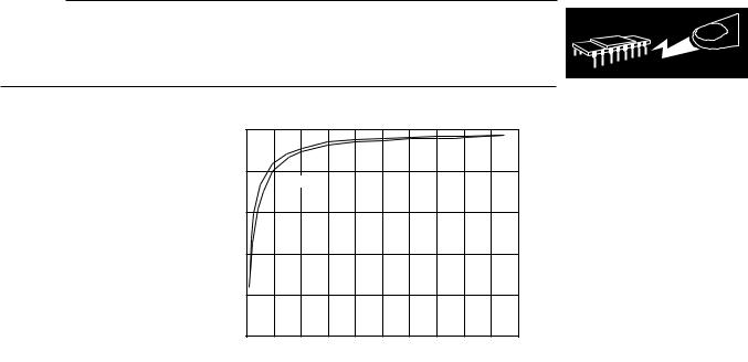
Figure 8. Output Voltage to Supply Rail vs. Load Current
|
|
|
|
|
|
|
|
|
VS = 5V |
|
|||
|
500 |
|
|
|
|
|
|
|
VCM = 2.5V |
|
|||
|
|
|
|
|
|
|
|
|
|||||
Amplifiers– |
|
|
|
|
|
|
|
|
TA = 25 C |
|
|||
400 |
|
|
|
|
|
|
|
|
|
|
|
|
|
|
|
|
|
|
|
|
|
|
|
|
|
|
|
QUANTITY |
300 |
|
|
|
|
|
|
|
|
|
|
|
|
|
|
|
|
|
|
|
|
|
|
|
|
||
200 |
|
|
|
|
|
|
|
|
|
|
|
|
|
|
|
|
|
|
|
|
|
|
|
|
|
|
|
|
100 |
|
|
|
|
|
|
|
|
|
|
|
|
|
|
|
|
|
|
|
|
|
|
|
|
|
|
|
|
|
|
|
|
|
|
|
|
|
|
|
|
|
|
–12 –10 –8 –6 –4 –2 0 2 4 |
|||||||||||
|
|
|
INPUT OFFSET VOLTAGE – mV |
||||||||||
Figure 3. Input Offset Voltage
|
Distribution |
|
|
|
|
|
|
VS = 5V |
|
|
|
|
|
|
TA = 25 C |
|
|
|
|
|
– pA |
8 |
|
|
|
|
|
7 |
|
|
|
|
|
|
CURRENT |
|
|
|
|
|
|
6 |
|
|
|
|
|
|
5 |
|
|
|
|
|
|
|
|
|
|
|
|
|
BIAS |
4 |
|
|
|
|
|
3 |
|
|
|
|
|
|
INPUT |
|
|
|
|
|
|
2 |
|
|
|
|
|
|
|
1 |
|
|
|
|
|
|
0 |
1 |
2 |
3 |
4 |
5 |
|
COMMON-MODE VOLTAGE – Volts |
|||||
Figure 6. Input Bias Current vs. Common-Mode Voltage
|
10000 |
|
|
|
|
|
|
|
VS = 5V |
|
|
|
|
|
1000 |
TA = 25 C |
|
|
|
|
– mV |
|
|
|
|
|
|
|
|
|
|
|
|
|
VOLTAGE |
100 |
|
SOURCE |
|
|
|
|
|
|
|
|||
|
|
|
|
|
||
OUTPUT |
10 |
|
|
SINK |
|
|
|
|
|
|
|
|
|
|
1 |
|
|
|
|
|
|
0.01 |
|
|
|
|
|
|
0.01 |
0.1 |
1 |
10 |
100 |
1000 |
|
|
|
LOAD CURRENT – mA |
|
|
|
Figure 9. Output Voltage to Supply Rail vs. Load Current
|
–2 |
|
|
|
|
VS = 5V |
|
– mV |
|
|
|
|
VCM = 2.5V |
||
|
|
|
|
|
|||
–3 |
|
|
|
|
|
|
|
VOLTAGE |
|
|
|
|
|
|
|
–4 |
|
|
|
|
|
|
|
–5 |
|
|
|
|
|
|
|
OFFSET |
|
|
|
|
|
|
|
–6 |
|
|
|
|
|
|
|
|
|
|
|
|
|
|
|
INPUT |
–7 |
|
|
|
|
|
|
–8 |
|
|
|
|
|
|
|
|
|
|
|
|
|
|
|
|
–35 |
–15 |
5 |
25 |
45 |
65 |
85 |
|
|
TEMPERATURE – C |
|
||||
Figure 4. Input Offset Voltage vs. Temperature
|
6 |
VS = 5V, 3V |
|
|
|
|
|
|
|
5 |
|
|
|
|
|
||
– pA |
VCM = VS/2 |
|
|
|
|
|
||
4 |
|
|
|
|
|
|
|
|
CURRENT |
|
|
|
|
|
|
|
|
3 |
|
|
|
|
|
|
|
|
2 |
|
|
|
|
|
|
|
|
OFFSET |
|
|
|
|
|
|
|
|
1 |
|
|
|
|
|
|
|
|
|
|
|
|
|
|
|
|
|
INPUT |
0 |
|
|
|
|
|
|
|
–1 |
|
|
|
|
|
|
|
|
|
|
|
|
|
|
|
|
|
|
–2 |
–35 |
–15 |
5 |
25 |
45 |
65 |
85 |
|
|
|||||||
|
|
|
TEMPERATURE – C |
|
||||
Figure 7. Input Offset Current vs.
|
Temperature |
|
|
|
|
||
|
|
VS = 2.7V |
|
|
|
|
|
|
|
RL = NO LOAD |
|
|
|
|
|
|
|
TA = 25 C |
|
|
|
|
– Degrees |
|
80 |
|
|
|
|
|
|
– dB |
60 |
|
|
|
|
45 |
|
40 |
|
|
|
|
90 |
||
GAIN |
|
|
|
|
SHIFT |
||
20 |
|
|
|
|
135 |
||
|
|
|
|
|
|
||
|
0 |
|
|
|
|
180 |
PHASE |
|
|
|
|
|
|
|
|
|
1k |
10k |
100k |
1M |
10M |
100M |
|
|
|
|
FREQUENCY – Hz |
|
|
|
|
Figure 10. Open-Loop Gain and Phase vs. Frequency
REV. C |
–5– |
 Loading...