


Analog Devices AD7305YR, AD7305BRU, AD7305BR, AD7305BN, AD7304YR Datasheet
...a |
+3 V/+5 V, Rail-to-Rail |
|
Quad, 8-Bit DAC |
||
|
|
|
|
|
AD7304/AD7305* |
|
|
|
FEATURES
Four 8-Bit DACs in One Package
+3 V, +5 V and 5 V Operation
Rail-to-Rail REF-Input to Voltage Output Swing 2.6 MHz Reference Multiplying Bandwidth
Compact 1.1 mm Height TSSOP 16-/20-Lead Package Internal Power ON Reset
SPI Serial Interface Compatible—AD7304 Fast Parallel Interface—AD7305
40 A Power Shutdown
APPLICATIONS
Automotive Output Span Voltage Instrumentation, Digitally Controlled Calibration
Pin-Compatible AD7226 Replacement when VDD < 5.5 V
GENERAL DESCRIPTION
The AD7304/AD7305 are quad, 8-bit DACs that operate from a single +3 V to +5 V supply or ±5 V supplies. The AD7304 has a serial interface, while the AD7305 has a parallel interface. Internal precision buffers swing rail-to-rail. The reference input range includes both supply rails allowing for positive or negative fullscale output voltages. Operation is guaranteed over the supply voltage range of +2.7 V to +5.5 V, consuming less than 9 mW from a +3 V supply.
The full-scale voltage output is determined by the external reference input voltage applied. The rail-to-rail VREF input to DAC VOUT allows for a full-scale voltage set equal the positive supply VDD, the negative supply VSS or any value in between.
The AD7304’s doubled-buffered serial-data interface offers high speed, three-wire, SPI and microcontroller compatible inputs using data in (SDI), clock (CLK) and chip select (CS) pins. Additionally, an internal power-on reset sets the output to zero scale.
The parallel input AD7305 uses a standard address decode along with the WR control line to load data into the input registers. The double buffered architecture allows all four input registers to be preloaded with new values, followed by a LDAC control strobe which copies all the new data into the DAC registers thereby updating the analog output values. When operating from less than +5.5 V, the AD7305 is pin-compatible with the popular industry standard AD7226.
FUNCTIONAL BLOCK DIAGRAMS
|
VDD |
|
|
|
VREFB VREFA |
|
|
PWR ON |
INPUT |
8 |
DAC A |
8 |
VOUTA |
|
RESET |
REG A |
|
REG |
DAC A |
|
|
|
8 |
8 |
|
8 |
|
|
|
INPUT |
DAC B |
VOUTB |
||
|
|
REG B |
|
REG |
DAC B |
|
CS |
|
INPUT |
8 |
DAC C |
8 |
VOUTC |
|
SERIAL |
REG C |
|
REG |
DAC C |
|
SDI/SHDN |
REG |
|
|
|
|
|
CLK |
|
INPUT |
8 |
DAC D |
8 |
VOUTD |
|
|
REG D |
|
REG |
DAC D |
|
|
|
|
|
|
AD7304 |
|
|
VSS |
GND |
CLR LDAC VREFC VREFD |
|
||
|
|
VDD |
|
|
VREF |
|
|
PWR ON |
INPUT |
8 |
DAC A |
8 |
VOUTA |
|
RESET |
REG A |
|
REG |
DAC A |
|
DB0 |
|
INPUT |
8 |
DAC B |
8 |
|
DB1 |
|
VOUTB |
||||
DB2 |
|
REG B |
|
REG |
DAC B |
|
DB3 |
|
INPUT |
8 |
DAC C |
8 |
|
DB4 |
|
|
||||
DB5 |
|
REG C |
|
REG |
DAC C |
VOUTC |
DB6 |
8 |
INPUT |
8 |
DAC D |
8 |
|
|
|
VOUTD |
||||
|
|
REG D |
|
REG |
DAC D |
|
WR |
|
|
|
|
|
|
A0/SHDN |
DECODE |
|
|
AD7305 |
||
A1 |
|
|
|
|
||
|
|
|
|
|
|
|
|
|
|
|
LDAC |
VSS |
GND |
An internal power ON reset places both parts in the zero-scale state at turn ON. A 40 A power shutdown (SHDN) feature is activated on both parts by tristating the SDI/SHDN pin on the AD7304, and tristating the A0/SHDN address pin on the AD7305.
The AD7304/AD7305 are specified over the extended industrial (–40°C to +85°C), and the automotive (–40°C to +125°C) temperature ranges. AD7304s are available in 16-lead plastic DIP (N-16), and wide-body SOL-16 (R-16) packages. The parallel input AD7305 is available in the 20-lead plastic DIP (N-20), and the SOL-20 (R-20) surface mount package. For ultracompact applications the thin 1.1 mm TSSOP-16 (RU-16) package will be available for the AD7304, while the TSSOP-20 (RU-20) will house the AD7305.
*Protected under Patent Number 5684481.
REV. A
Information furnished by Analog Devices is believed to be accurate and reliable. However, no responsibility is assumed by Analog Devices for its use, nor for any infringements of patents or other rights of third parties which may result from its use. No license is granted by implication or otherwise under any patent or patent rights of Analog Devices.
One Technology Way, P.O. Box 9106, Norwood, MA 02062-9106, U.S.A.
Tel: 781/329-4700 |
World Wide Web Site: http://www.analog.com |
Fax: 781/326-8703 |
© Analog Devices, Inc., 1998 |
|
|
(@ VDD = +3 V or +5 V, VSS = 0 V; or VDD = +5 V and VSS = –5 V, VSS |
||||
AD7304/AD7305–SPECIFICATIONS ≤ VREF ≤ VDD, –40 C < TA < +85 C/+125 C, unless otherwise noted.) |
||||||
Parameter |
Symbol |
Condition |
3 V 10% |
5 V 10% |
5 V 10% |
Units |
|
|
|
|
|
|
|
STATIC PERFORMANCE |
|
|
|
|
|
|
Resolution1 |
N |
|
8 |
8 |
8 |
Bits |
Integral Nonlinearity2 |
INL |
|
± 1 |
± 1 |
± 1 |
LSB max |
Differential Nonlinearity |
DNL |
Monotonic, All Codes 0 to FFH |
± 1 |
± 1 |
± 1 |
LSB max |
Zero-Scale Error |
VZSE |
Data = 00H |
15 |
15 |
± 15 |
mV max |
Full-Scale Voltage Error |
VFSE |
Data = FFH |
± 4 |
± 4 |
± 4 |
LSB max |
Full-Scale Tempco3 |
TCVFS |
|
5 |
5 |
5 |
ppm/°C typ4 |
REFERENCE INPUT |
|
|
|
|
|
|
VREFIN Range |
VREFIN |
|
VSS/VDD |
VSS/VDD |
VSS/VDD |
V min/max |
Input Resistance (AD7304) |
RREFIN |
Code = 55H |
28 |
28 |
28 |
kΩ typ |
Input Resistance (AD7305) |
RREFIN |
All DACs at Code = 55H |
7.5 |
7.5 |
7.5 |
kΩ typ |
Input Capacitance3 |
CREFIN |
|
5 |
5 |
5 |
pF typ |
ANALOG OUTPUTS |
|
|
|
|
|
|
Output Voltage Range |
VOUT |
|
VSS/VDD |
VSS/VDD |
VSS/VDD |
V min/max |
Output Current Drive |
IOUT |
Code = 80H, ∆VOUT < 1 LSB |
± 3 |
± 3 |
± 3 |
mA typ |
Shutdown Resistance |
ROUT |
DAC Outputs Placed in Shutdown State |
120 |
120 |
120 |
kΩ typ |
Capacitive Load3 |
CL |
No Oscillation |
200 |
200 |
200 |
pF typ |
LOGIC INPUTS |
|
|
|
|
|
|
Logic Input Low Voltage |
VIL |
|
0.6 |
0.8 |
0.8 |
V min |
Logic Input High Voltage |
VIH |
|
2.1 |
2.4 |
2.4 |
V max |
Input Leakage Current5 |
IIL |
|
± 10 |
± 10 |
± 10 |
µA max |
Input Capacitance3 |
CIL |
|
8 |
8 |
8 |
pF max |
AC CHARACTERISTICS3 |
|
|
|
|
|
|
Output Slew Rate |
SR |
Code = 00H to FFH to 00H |
1/2.7 |
1/3.6 |
1/3.6 |
V/µs min/typ |
Reference Multiplying |
BW |
Small Signal, VSS = –5 V |
|
|
2.6 |
MHz typ |
Total Harmonic Distortion |
THD |
VREF = 4 V p-p, VSS = –5 V, f = 1 kHz |
|
|
0.025 |
% |
Settling Time6 |
tS |
To ±0.1% of Full Scale |
1.1/2 |
1.0/2 |
1.0/2 |
µs typ/max |
Shutdown Recovery Time |
tSDR |
To ±0.1% of Full Scale |
2 |
2 |
2 |
µs max |
Time to Shutdown |
tSDN |
|
15 |
15 |
15 |
µs typ |
DAC Glitch |
Q |
|
15 |
15 |
15 |
nVs typ |
Digital Feedthrough |
Q |
|
2 |
2 |
2 |
nVs typ |
Feedthrough |
VOUT/VREF |
Code = 00H, VREF =1 V p-p, f = 100 kHz |
|
|
–65 |
dB |
SUPPLY CHARACTERISTICS |
|
|
|
|
|
|
Positive Supply Current |
IDD |
VLOGIC = 0 V or VDD, No Load |
6 |
6 |
6 |
mA max |
Negative Supply Current |
ISS |
VSS = –5 V |
|
|
6 |
mA max |
Power Dissipation |
PDISS |
VLOGIC = 0 V or VDD, No Load |
15 |
30 |
60 |
mW max |
Power Down |
IDD_SD |
SDI/SHDN = Floating |
40 |
40 |
40 |
µA typ |
Power Supply Sensitivity |
PSS |
∆VDD = ±10% |
0.004 |
0.004 |
0.004 |
%/% |
NOTES
1One LSB = VREF/256.
2The first three codes (00H, 01H, 10H) are excluded from the integral nonlinearity error measurement in single supply operation +3 V or +5 V. 3These parameters are guaranteed by design and not subject to production testing.
4Typicals represent average readings measured at +25°C.
5SDI/SHDN and A0/SHDN pins have 30 A maximum IIL input leakage current.
6The settling time specification does not apply for negative going transitions within the last 3 LSBs of ground in single supply operation.
Specifications subject to change without notice.
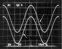
5V
|
VREF = 10V p-p |
|
f = 20kHz |
5V |
0V |
|
|
0V |
|
|
–5V |
|
VOUT = 10V p-p |
–5V |
|
(OUT) |
(IN) |
Figure 1. AD7304/AD7305 Rail-to-Rail Reference Input to Output at 20 kHz
–2– |
REV. A |

AD7304/AD7305
TIMING SPECIFICATIONS |
(@ VDD = +3 V or +5 V, VSS = 0 V; or VDD = +5 V and VSS = –5 V, VSS ≤ VREF ≤ VDD, –40 C < TA < |
||||||
+85 C/125 C, unless otherwise noted.) |
|
|
|
||||
|
|
|
|
|
|
|
|
Parameter |
Symbol |
3 V 10% |
|
5 V 10% |
5 V 10% |
Units |
|
|
|
|
|
|
|
|
|
INTERFACE TIMING SPECIFICATIONS1, 2 |
|
|
|
|
|
||
AD7304 Only |
|
|
70 |
|
55 |
55 |
ns min |
Clock Width High |
tCH |
|
|
||||
Clock Width Low |
tCL |
|
70 |
|
55 |
55 |
ns min |
Data Setup |
tDS |
|
50 |
|
40 |
40 |
ns min |
Data Hold |
tDH |
|
30 |
|
20 |
20 |
ns min |
Load Pulsewidth |
tLDW |
|
70 |
|
60 |
60 |
ns min |
Load Setup |
tLD1 |
|
40 |
|
30 |
30 |
ns min |
Load Hold |
tLD2 |
|
40 |
|
30 |
30 |
ns min |
Clear Pulsewidth |
tCLWR |
|
60 |
|
60 |
60 |
ns min |
Select |
tCSS |
|
30 |
|
20 |
20 |
ns min |
Deselect |
tCSH |
|
60 |
|
40 |
40 |
ns min |
AD7305 Only |
|
|
|
|
|
|
|
Data Setup |
tDS |
|
60 |
|
40 |
40 |
ns min |
Data Hold |
tDH |
|
30 |
|
20 |
20 |
ns min |
Address Setup |
tAS |
|
60 |
|
40 |
40 |
ns min |
Address Hold |
tAH |
|
30 |
|
20 |
20 |
ns min |
Write Width |
tWR |
|
60 |
|
50 |
50 |
ns min |
Load Pulsewidth |
tLDW |
|
60 |
|
50 |
50 |
ns min |
Load Setup |
tLS |
|
60 |
|
40 |
40 |
ns min |
Load Hold |
tLH |
|
30 |
|
20 |
20 |
ns min |
NOTES
1These parameters are guaranteed by design and not subject to production testing.
2All input control signals are specified with tR = tF = 2 ns (10% to 90% of VDD) and timed from a voltage level of 1.6 V.
ABSOLUTE MAXIMUM RATINGS* |
|
VDD to GND . . . . . . . . . . . . . . . . . . . . . . |
. . . . . . –0.3 V, +8 V |
VSS to GND . . . . . . . . . . . . . . . . . . . . . . . . |
. . . . . +0.3 V, –8 V |
VREFX to GND . . . . . . . . . . . . . . . . . . . . . . |
. . . . . . . . VSS, VDD |
Logic Inputs to GND . . . . . . . . . . . . . . . |
–0.3 V, VDD + 0.3 V |
VOUTX to GND . . . . . . . . . . . . . . . . . . . . |
–0.3 V, VDD + 0.3 V |
IOUT Short Circuit to GND . . . . . . . . . . . . |
. . . . . . . . . 50 mA |
Package Power Dissipation . . . . . . . . . . . . |
. . (TJ MAX–TA)/θJA |
Thermal Resistance θJA |
103°C/W |
16-Lead Plastic DIP Package (N-16) . . . |
|
16-Lead SOIC Package (R-16) . . . . . . . |
. . . . . . . . 73°C/W |
TSSOP-16 Package (RU-16) . . . . . . . . . |
. . . . . . . 180°C/W |
20-Lead Plastic DIP Package (N-20) . . . |
. . . . . . . 120°C/W |
20-Lead SOIC Package (R-20) . . . . . . . |
. . . . . . . . 74°C/W |
TSSOP-20 Package (RU-20) . . . . . . . . . |
. . . . . . . 155°C/W |
Maximum Junction Temperature (TJ MAX) |
. . . . . . . . . +150°C |
Operating Temperature Range . . . . . . . . . |
. . –40°C to +85°C |
Storage Temperature Range . . . . . . . . . . . |
. –65°C to +150°C |
Lead Temperature |
+300°C |
N-16 and N-20 (Soldering, 10 secs) . . . |
R-16, R-20, RU-16, RU-20 (Vapor Phase, 60 secs) . . +215°C R-16, R-20, RU-16, RU-20 (Infrared, 15 secs) . . . . +220°C
*Stresses above those listed under Absolute Maximum Ratings may cause permanent damage to the device. This is a stress rating only; functional operation of the device at these or any other conditions above those indicated in the operational sections of this specification is not implied. Exposure to absolute maximum rating conditions for extended periods may affect device reliability.
ORDERING GUIDE
|
Temperature |
Package |
Package |
Model |
Range |
Description |
Options |
|
|
|
|
AD7304BN |
–40°C/+85°C |
16-Lead P-DIP |
N-16 |
AD7304BR |
–40°C/+85°C |
16-Lead SOIC |
R-16 |
AD7304YR |
–40°C/+125°C |
16-Lead SOIC |
R-16 |
AD7304BRU |
–40°C/+85°C |
TSSOP-16 |
RU-16 |
AD7305BN |
–40°C/+85°C |
20-Lead P-DIP |
N-20 |
AD7305BR |
–40°C/+85°C |
20-Lead SOIC |
R-20 |
AD7305YR |
–40°C/+125°C |
20-Lead SOIC |
R-20 |
AD7305BRU |
–40°C/+85°C |
TSSOP-20 |
RU-20 |
|
|
|
|
The AD7304/AD7305 contains 2759 transistors. Die size: 103 mil × 102 mil, 10,506 sq mil.
CAUTION
ESD (electrostatic discharge) sensitive device. Electrostatic charges as high as 4000 V readily accumulate on the human body and test equipment and can discharge without detection. Although the AD7304/AD7305 features proprietary ESD protection circuitry, permanent damage may occur on devices subjected to high energy electrostatic discharges. Therefore, proper ESD precautions are recommended to avoid performance degradation or loss of functionality.
WARNING!
ESD SENSITIVE DEVICE
REV. A |
–3– |

AD7304/AD7305 |
|
|
|
|
|
|
|
|
|
|
|
|
SDI |
SA |
SI |
A1 |
A0 |
D7 |
D6 |
D5 |
D4 |
D3 |
D2 |
D1 |
D0 |
CLK |
|
|
|
|
|
|
|
|
|
|
|
|
|
|
tCSS |
|
|
|
|
|
|
|
|
tCSH |
|
CS |
|
|
|
|
|
|
|
|
|
|
|
|
|
|
|
|
|
|
|
|
|
|
|
|
tLD2 |
LDAC |
tLD1 |
|
|
|
|
|
|
|
|
|
|
|
SDI |
|
|
|
|
|
|
|
|
|
|
|
|
|
|
|
|
tDS |
tDH |
|
|
|
|
|
|
|
CLK |
|
|
tCL |
|
tCH |
|
|
|
|
|
|
|
|
|
|
|
|
|
|
|
|
|
|
|
|
LDAC |
|
|
|
|
|
|
|
tLDW |
|
|
|
|
CLR |
|
|
|
|
|
|
|
tS |
|
|
|
tCLRW |
FS |
|
|
|
|
|
|
|
|
|
|
1 LSB |
|
VOUT |
|
|
|
|
|
|
|
|
|
|
|
|
|
|
|
|
|
|
|
|
|
ERROR BAND |
|||
ZS |
|
|
|
|
|
|
|
|
|
|
|
|
|
|
|
|
|
|
|
|
|
|
|
|
tS |
Figure 2. AD7304 Timing Diagram
|
tSDN |
SDI/SHDN |
tSDR |
IDD |
|
Figure 3. AD7304 Timing Diagram
Table I. AD7304 Control Logic Truth Table
CS |
CLK |
LDAC |
CLR |
Serial Shift Register Function |
Input REG Function |
DAC Register Function |
|
|
|
|
|
|
|
H |
X |
H |
H |
No Effect |
No Effect |
No Effect |
L |
↑+ |
H |
H |
Data Advanced 1 Bit |
No Effect |
No Effect |
↑+ |
L |
H |
H |
No Effect |
Updated with SR Contents2 |
No Effect |
H |
X |
L |
H |
No Effect |
Latched with SR Contents2 |
All Input Register Contents Transferred3 |
H |
X |
H |
↓– |
No Effect |
Loaded with 00H |
Loaded with 00H |
H |
X |
H |
↑+ |
No Effect |
Latched with 00H |
Latched with 00H |
NOTES
1↑+ positive logic transition; ↓– negative logic transition; X Don’t Care.
2One Input Register receives the data bits D7–D0 decoded from the SR address bits (A1, A0); where REG A = (0, 0); B = (0, 1); C = (1, 0); D = (1, 1). 3LDAC is a level-sensitive input.
Table II. AD7304 Serial Input Register Data Format, Data Is Loaded in the MSB-First Format
|
MSB |
|
|
|
|
|
|
|
|
|
|
LSB |
|
B11 |
B10 |
B9 |
B8 |
B7 |
B6 |
B5 |
B4 |
B3 |
B2 |
B1 |
B0 |
|
|
|
|
|
|
|
|
|
|
|
|
|
AD7304 |
SAC |
SDC |
A1 |
A0 |
D7 |
D6 |
D5 |
D4 |
D3 |
D2 |
D1 |
D0 |
|
|
|
|
|
|
|
|
|
|
|
|
|
If B11 (SAC), Shutdown All Channels, is set to logic LOW, all DACs are placed in a power shutdown mode, all output voltages become high resistance. If B10 (SDC), Shutdown Decoded Channel, is set to logic LOW, only the DAC decoded by address bits A1 and A0 is placed in the shutdown mode.
–4– |
REV. A |

|
|
|
|
|
AD7304/AD7305 |
|
|
|
|
|
|
|
|
|
|
|
|
Table III. AD7305 Control Logic Truth Table |
||
|
|
|
|
|
|
|
WR |
A1 |
A0 |
LDAC |
Input Register Function |
DAC Register Function |
|
|
|
|
|
|
|
|
L |
L |
L |
H |
REG A Loaded with DB0–DB7 |
Latched with Previous Contents, No Change |
|
↑+ |
L |
L |
H |
REG A Latched with DB0–DB7 |
Latched with Previous Contents, No Change |
|
L |
L |
H |
H |
REG B Loaded with DB0–DB7 |
Latched with Previous Contents, No Change |
|
↑+ |
L |
H |
H |
REG B Latched with DB0–DB7 |
Latched with Previous Contents, No Change |
|
L |
H |
L |
H |
REG C Loaded with DB0–DB7 |
Latched with Previous Contents, No Change |
|
↑+ |
H |
L |
H |
REG C Latched with DB0–DB7 |
Latched with Previous Contents, No Change |
|
L |
H |
H |
H |
REG D Loaded with DB0–DB7 |
Latched with Previous Contents, No Change |
|
↑+ |
H |
H |
H |
REG D Latched with DB0–DB7 |
Latched with Previous Contents, No Change |
|
H |
X |
X |
L |
No Effect |
All Input Register Contents Loaded, Register Transparent |
|
L |
X |
X |
L |
Input REG x Transparent to DB0–DB7 |
Register Transparent |
|
H |
X |
X |
↑+ |
No Effect |
All Input Register Contents Latched |
|
H |
X |
X |
H |
No Effect, Device Not Selected |
No Effect, Device Not Selected |
|
|
|
|
|
|
|
|
NOTES |
|
1↑+ positive logic transition; ↓– negative logic transition; X Don’t Care. |
PIN CONFIGURATIONS |
2LDAC is a level sensitive input. |
tWR |
|
|
WR |
|
|
tAS |
tAH |
|
A0, A1 |
|
|
tDS |
tDH |
|
D0–D7 |
|
|
tLS |
tLH |
tLDW |
LDAC |
|
|
|
tS |
|
VOUT |
|
1 LSB |
|
ERROR BAND |
Figure 4. AD7305 Timing Diagram
|
tSDN |
A0/SHDN |
tSDR |
IDD |
|
Figure 5. AD7305 Timing Diagram
|
|
|
|
|
|
|
VOUTB |
|
|
|
VOUTC |
|
|
|
|
|
|
|
1 |
|
20 |
||
VOUTB |
1 |
|
16 |
VOUTC |
VOUTA |
2 |
|
19 |
VOUTD |
||
|
|
|
|
|
VSS |
|
|
|
VDD |
||
VOUTA |
2 |
|
15 |
VOUTD |
3 |
|
18 |
||||
|
|
|
|
|
|
VREF |
|
|
|
A0/SHDN |
|
VSS |
3 |
|
14 |
VDD |
|
4 |
|
17 |
|||
|
|
AD7304 |
|
|
GND |
|
AD7305 |
|
A1 |
||
VREFA |
4 |
13 |
VREFC |
5 |
16 |
||||||
VREFB |
|
TOP VIEW |
|
|
|
|
|
|
TOP VIEW |
|
|
5 |
(Not to Scale) |
12 |
V |
REF |
D |
LDAC |
6 |
(Not to Scale) |
15 |
WR |
|
|
|
|
|
|
|
|
|
DB0 |
|||
GND |
6 |
|
11 |
SDI/SHDN |
DB7 |
7 |
|
14 |
|||
|
|
|
|
|
|
DB6 |
|
|
|
DB1 |
|
LDAC |
7 |
|
10 |
CLK |
|
8 |
|
13 |
|||
|
|
|
|
|
|
|
DB5 |
|
|
|
DB2 |
CLR |
8 |
|
9 |
CS |
|
9 |
|
12 |
|||
|
|
|
|
|
|
|
|
|
|
|
|
|
|
|
|
|
|
|
DB4 |
10 |
|
11 |
DB3 |
|
|
|
|
|
|
|
|
||||
|
|
|
|
|
|
|
|
|
|
|
|
REV. A |
–5– |
 Loading...