


 Loading...
Analog Devices AD7741BN, AD7742YR, AD7742BR, AD7742BN, AD7741YR Datasheet
...
a |
Single and Multichannel, Synchronous |
|
Voltage-to-Frequency Converters |
||
|
|
AD7741/AD7742 |
|
|
|
FEATURES
AD7741: One Single-Ended Input Channel
AD7742: Two Differential or Three Pseudo-Differential Input Channels
Integral Nonlinearity of 0.012% at fOUT(Max) = 2.75 MHz (AD7742) and at fOUT(Max) = 1.35 MHz (AD7741)
Single +5 V Supply Operation Buffered Inputs
Programmable Gain Analog Front-End On-Chip +2.5 V Reference Internal/External Reference Option Power Down to 35 mA Max
Minimal External Components Required 8-Lead and 16-Lead DIP and SOIC Packages
APPLICATIONS
Low Cost Analog-to-Digital Conversion
Signal Isolation
GENERAL DESCRIPTION
The AD7741/AD7742 are a new generation of synchronous voltage-to-frequency converters (VFCs). The AD7741 is a single-channel version in an 8-lead package (SOIC/DIP) and the AD7742 is a multichannel version in a 16-lead package (SOIC/ DIP). No user trimming is required to achieve the specified performance.
The AD7741 has a single buffered input whereas the AD7742 has four buffered inputs that may be configured as two fullydifferential inputs or three pseudo-differential inputs. Both parts include an on-chip +2.5 V bandgap reference that provides the user with the option of using this internal reference or an external reference.
|
FUNCTIONAL BLOCK DIAGRAMS |
|||||
|
VDD |
REFIN/OUT |
|
PD |
||
|
|
|
|
+2.5V |
|
|
|
|
|
|
REFERENCE |
POWER-DOWN |
|
|
|
|
|
|
|
LOGIC |
|
|
|
VOLTAGE-TO- |
|
fOUT |
|
VIN |
X1 |
|
FREQUENCY |
|
||
|
|
|
MODULATOR |
|
|
|
|
|
CLOCK |
|
|
AD7741 |
|
|
|
|
|
|
||
|
|
GENERATION |
|
|
||
|
CLKIN |
CLKOUT |
GND |
|
||
|
VDD |
|
|
UNI/BIP |
|
PD |
GAIN |
|
|
|
AD7742 |
|
|
|
|
|
|
POWER-DOWN |
||
|
|
|
|
|
|
|
VIN1 |
|
|
|
|
|
LOGIC |
VIN2 |
INPUT |
X1/X2 |
|
VOLTAGE-TO- |
fOUT |
|
|
MUX |
|
FREQUENCY |
|||
VIN3 |
|
|
MODULATOR |
|
||
|
|
|
|
|||
VIN4 |
|
|
|
|
|
|
A1 |
|
|
CLOCK |
|
+2.5V |
|
|
GENERATION |
|
REFERENCE |
|||
|
|
|
||||
A0 |
|
|
|
|
|
|
|
GND |
CLKIN |
CLKOUT |
REFIN |
REFOUT |
|
The AD7741 has a single-ended voltage input range from 0 V to REFIN. The AD7742 has a differential voltage input range from –VREF to +VREF. Both parts operate from a single +5 V supply consuming typically 6 mA, and also contain a powerdown feature that reduces the current consumption to less than 35 A.
REV. 0
Information furnished by Analog Devices is believed to be accurate and reliable. However, no responsibility is assumed by Analog Devices for its use, nor for any infringements of patents or other rights of third parties which may result from its use. No license is granted by implication or otherwise under any patent or patent rights of Analog Devices.
One Technology Way, P.O. Box 9106, Norwood, MA 02062-9106, U.S.A.
Tel: 781/329-4700 |
World Wide Web Site: http://www.analog.com |
Fax: 781/326-8703 |
© Analog Devices, Inc., 1999 |
AD7741–SPECIFICATIONS |
(VDD = +4.75 V to +5.25 V; VREF = +2.5 V; fCLKIN = 6.144 MHz; all specifications TMIN to |
||||
TMAX unless otherwise noted.) |
|
||||
Parameter2 |
B and Y Version1 |
|
|
||
Min |
Typ |
Max |
Units |
Conditions/Comments |
|
DC PERFORMANCE |
|
|
|
|
|
Integral Nonlinearity |
|
|
± 0.012 |
|
|
fCLKIN = 200 kHz3 |
|
|
% of Span4 |
|
|
fCLKIN = 3 MHz3 |
|
|
± 0.012 |
% of Span |
|
fCLKIN = 6.144 MHz |
|
|
± 0.024 |
% of Span |
VDD > 4.8 V |
Offset Error |
|
|
± 40 |
mV |
|
Gain Error |
0 |
+0.8 |
+1.6 |
% of Span |
|
Offset Error Drift3 |
|
± 30 |
|
µV/°C |
|
Gain Error Drift3 |
|
± 16 |
|
ppm of Span/°C |
VDD = ± 5% |
Power Supply Rejection Ratio3 |
|
–63 |
|
dB |
|
ANALOG INPUT5 |
|
± 50 |
± 100 |
|
|
Input Current |
|
nA |
|
||
Input Voltage Range |
0 |
|
VREF |
V |
|
+2.5 V REFERENCE (REFIN/OUT) |
|
|
|
|
|
REFIN |
|
|
|
|
|
Nominal Input Voltage |
|
2.5 |
|
V |
|
Input Impedance6 |
|
N/A |
|
|
|
REFOUT |
|
|
|
|
|
Output Voltage |
2.38 |
2.50 |
2.60 |
V |
|
Output Impedance3 |
|
1 |
|
kΩ |
|
Reference Drift3 |
|
± 50 |
|
ppm/°C |
|
Line Rejection |
|
–60 |
|
dB |
|
Reference Noise (0.1 Hz to 10 Hz)3 |
|
100 |
|
µV p-p |
|
LOGIC OUTPUT |
|
|
|
|
Output Sourcing 800 µA7 |
Output High Voltage, VOH |
4.0 |
|
|
V |
|
Output Low Voltage, VOL |
|
|
0.4 |
V |
Output Sinking 1.6 mA7 |
Minimum Output Frequency |
|
0.05 fCLKIN |
|
Hz |
VIN = 0 V |
Maximum Output Frequency |
|
0.45 fCLKIN |
|
Hz |
VIN = VREF |
LOGIC INPUT |
|
|
|
|
|
PD ONLY |
|
|
|
|
|
Input High Voltage, VIH |
2.4 |
|
|
V |
|
Input Low Voltage, VIL |
|
|
0.8 |
V |
|
Input Current |
|
|
± 100 |
nA |
|
Pin Capacitance |
|
6 |
10 |
pF |
|
CLKIN ONLY |
|
|
|
|
|
Input High Voltage, VIH |
3.5 |
|
|
V |
|
Input Low Voltage, VIL |
|
|
0.8 |
V |
|
Input Current |
|
|
± 2 |
µA |
|
Pin Capacitance |
|
6 |
10 |
pF |
|
|
|
|
|
|
|
CLOCK FREQUENCY |
|
|
|
|
|
Input Frequency |
|
|
6.144 |
MHz |
For Specified Performance |
|
|
|
|
|
|
POWER REQUIREMENTS |
|
|
|
|
|
VDD |
4.75 |
|
5.25 |
V |
|
IDD (Normal Mode) |
|
|
8 |
mA |
Output Unloaded |
IDD (Power-Down) |
|
15 |
35 |
µA |
|
Power-Up Time3 |
|
30 |
|
µs |
Coming Out of Power-Down Mode |
NOTES
1Temperature ranges: B Version –40°C to +85°C: Y Version: –40°C to +105°C. 2See Terminology.
3Guaranteed by design and characterization, not production tested.
4Span = Maximum Output Frequency–Minimum Output Frequency.
5The absolute voltage on the input pin must not go more positive than VDD – 2.25 V or more negative than GND.
6Because this pin is bidirectional, any external reference must be capable of sinking/sourcing 400 A in order to overdrive the internal reference. 7These logic levels apply to CLKOUT only when it is loaded with one CMOS load.
Specifications subject to change without notice.
–2– |
REV. 0 |
|
|
|
|
|
|
|
|
AD7741/AD7742 |
||
AD7742–SPECIFICATIONS |
(VDD = +4.75 V to +5.25 V; VREF = +2.5 V; fCLKIN = 6.144 MHz; all specifications TMIN to |
|||||||||
TMAX unless otherwise noted.) |
|
|
|
|
||||||
Parameter3 |
B Version1 |
|
|
Y Version2 |
|
|
|
|
||
Min |
Typ |
Max |
|
Min |
Typ |
Max |
Units |
Conditions/Comments |
||
DC PERFORMANCE |
|
|
|
|
|
|
|
|
|
|
Integral Nonlinearity |
|
|
± 0.0122 |
|
|
|
± 0.015 |
|
|
|
fCLKIN = 200 kHz4 |
|
|
|
|
|
% of Span5 |
|
|
||
fCLKIN = 3 MHz4 |
|
|
± 0.0122 |
|
|
|
± 0.015 |
% of Span |
|
|
fCLKIN = 6.144 MHz |
|
|
± 0.0122 |
|
|
|
± 0.015 |
% of Span |
|
|
Offset Error |
|
|
± 40 |
|
|
|
± 40 |
mV |
Unipolar Mode |
|
|
|
|
± 40 |
|
|
|
± 40 |
mV |
Bipolar Mode |
|
Gain Error |
+0.2 |
+1.2 |
+2.2 |
|
+0.2 |
+1.2 |
+2.2 |
% of Span |
Unipolar Mode |
|
|
+0.2 |
+1.2 |
+2.2 |
|
+0.2 |
+1.2 |
+2.2 |
% of Span |
Bipolar Mode |
|
Offset Error Drift4 |
|
± 12 |
|
|
|
± 12 |
|
µV/°C |
Unipolar Mode |
|
|
|
± 12 |
|
|
|
± 12 |
|
µV/°C |
Bipolar Mode |
|
Gain Error Drift4 |
|
± 2 |
|
|
|
± 2 |
|
ppm of Span/°C |
Unipolar Mode |
|
|
|
± 4 |
|
|
|
± 4 |
|
ppm of Span/°C |
Bipolar Mode |
|
Power Supply Rejection Ratio4 |
|
–70 |
|
|
|
–70 |
|
dB |
VDD = ± 5% |
|
Channel-to-Channel Isolation4 |
|
–75 |
|
|
|
–75 |
|
dB |
|
|
Common-Mode Rejection |
–60 |
–78 |
|
|
–58 |
–78 |
|
dB |
|
|
|
|
|
|
|
|
|
|
|
|
|
ANALOG INPUTS (VIN1–VIN4)6 |
|
± 50 |
± 100 |
|
|
± 50 |
± 100 |
|
|
|
Input Current |
|
|
|
nA |
|
|
||||
Common-Mode Input Range |
+0.5 |
|
VDD – 1.75 |
|
+0.5 |
|
VDD – 1.75 |
V |
|
|
Differential Input Range |
–VREF/Gain |
|
+VREF/Gain |
–VREF/Gain |
|
+VREF/Gain |
V |
Bipolar Mode |
||
|
0 |
|
+VREF/Gain |
|
0 |
|
+VREF/Gain |
V |
Unipolar Mode |
|
VOLTAGE REFERENCE |
|
|
|
|
|
|
|
|
|
|
REFIN |
|
|
|
|
|
|
|
|
|
|
Nominal Input Voltage |
|
2.5 |
|
|
|
2.5 |
|
V |
|
|
Input Impedance4 |
|
|
|
|
|
|
|
kΩ |
|
|
fCLKIN = 3 MHz |
70 |
|
|
|
70 |
|
|
|
|
|
fCLKIN = 6.144 MHz |
35 |
|
|
|
35 |
|
|
kΩ |
|
|
REFOUT |
|
|
|
|
|
|
|
|
|
|
Output Voltage |
2.38 |
2.50 |
2.60 |
|
2.38 |
2.50 |
2.60 |
V |
|
|
Output Impedance4 |
|
1 |
|
|
|
1 |
|
kΩ |
|
|
Reference Drift4 |
|
± 50 |
|
|
|
± 50 |
|
ppm/°C |
|
|
Line Rejection |
|
–70 |
|
|
|
–70 |
|
dB |
|
|
Reference Noise |
|
|
|
|
|
|
|
µV p-p |
|
|
(0.1 Hz to 10 Hz)4 |
|
100 |
|
|
|
100 |
|
|
|
|
LOGIC OUTPUT |
|
|
|
|
|
|
|
|
Output Sourcing 800 µA7 |
|
Output High Voltage, VOH |
4.0 |
|
|
|
4.0 |
|
|
V |
||
Output Low Voltage, VOL |
|
|
0.4 |
|
|
|
0.4 |
V |
Output Sinking 1.6 mA7 |
|
Minimum Output Frequency |
|
0.05 fCLKIN |
|
|
|
0.05 fCLKIN |
|
Hz |
VIN = 0 V (Unipolar), VIN = |
|
|
|
|
|
|
|
|
|
|
–VREF/Gain (Bipolar) |
|
Maximum Output Frequency |
|
0.45 fCLKIN |
|
|
|
0.45 fCLKIN |
|
Hz |
VIN = VREF/Gain (Unipolar |
|
|
|
|
|
|
|
|
|
|
and Bipolar) |
|
|
|
|
|
|
|
|
|
|
|
|
LOGIC INPUT |
|
|
|
|
|
|
|
|
|
|
ALL EXCEPT CLKIN |
|
|
|
|
|
|
|
|
|
|
Input High Voltage, VIH |
2.4 |
|
|
|
2.4 |
|
|
V |
|
|
Input Low Voltage, VIL |
|
|
0.8 |
|
|
|
0.8 |
V |
|
|
Input Current |
|
|
± 100 |
|
|
|
± 100 |
nA |
|
|
Pin Capacitance |
|
6 |
10 |
|
|
6 |
10 |
pF |
|
|
CLKIN ONLY |
|
|
|
|
|
|
|
|
|
|
Input High Voltage, VIH |
3.5 |
|
|
|
3.5 |
|
|
V |
|
|
Input Low Voltage, VIL |
|
|
0.8 |
|
|
|
0.8 |
V |
|
|
Input Current |
|
|
± 2 |
|
|
|
± 2 |
µA |
|
|
Pin Capacitance |
|
6 |
10 |
|
|
6 |
10 |
pF |
|
|
|
|
|
|
|
|
|
|
|
|
|
CLOCK FREQUENCY |
|
|
|
|
|
|
|
|
|
|
Input Frequency |
|
|
6.144 |
|
|
|
6.144 |
MHz |
For Specified Performance |
|
|
|
|
|
|
|
|
|
|
|
|
POWER REQUIREMENTS |
|
|
|
|
|
|
|
|
|
|
VDD |
4.75 |
|
5.25 |
|
4.75 |
|
5.25 |
V |
|
|
IDD (Normal Mode) |
|
6 |
8 |
|
|
6 |
8 |
mA |
Output Unloaded |
|
IDD (Power-Down) |
|
25 |
35 |
|
|
25 |
35 |
µA |
|
|
Power-Up Time4 |
|
30 |
|
|
|
30 |
|
µs |
Coming Out of Power- |
|
|
|
|
|
|
|
|
|
|
Down Mode |
|
|
|
|
|
|
|
|
|
|
|
|
NOTES |
|
|
|
|
|
|
|
|
|
|
1Temperature range: B Version: –40°C to +85°C. |
|
|
|
|
|
|
|
|
|
|
2Temperature range: Y Version: –40°C to +105°C. |
|
|
|
|
|
|
|
|
|
|
3See Terminology. |
|
|
|
|
|
|
|
|
|
|
4Guaranteed by design and characterization, not production tested. |
|
|
|
|
|
|
|
|
||
5Span = Maximum Output Frequency–Minimum Output Frequency. |
|
|
|
|
|
|
|
|
||
6The absolute voltage on the input pins must not go more positive than VDD – 1.75 V or more negative than +0.5 V. |
|
|
|
|||||||
7These logic levels apply to CLKOUT only when it is loaded with one CMOS load. |
|
|
|
|
|
|
||||
Specifications subject to change without notice.
REV. 0 |
–3– |
AD7741/AD7742
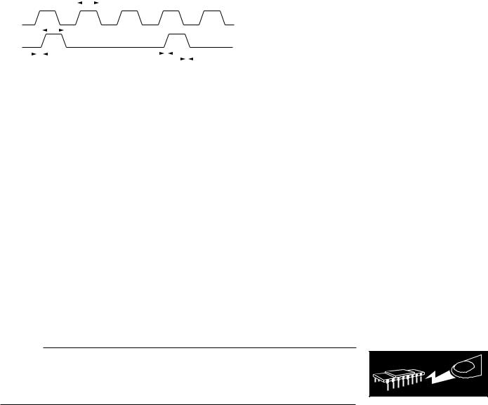
TIMING CHARACTERISTICS1, 2, 3
(VDD = +4.75 V to +5.25 V; VREF = +2.5 V. All specifications TMIN to TMAX unless otherwise noted.)
|
Limit at TMIN, TMAX |
|
|
Parameter |
(B and Y Version) |
Units |
Conditions/Comments |
|
|
|
|
fCLKIN |
6.144 |
MHz max |
|
tHIGH/tLOW |
55/45 |
max |
Input Clock Mark/Space Ratio |
|
45/55 |
min |
|
t1 |
9 |
ns typ |
fCLOCK Rising Edge to fOUT Rising Edge |
t2 |
4 |
ns typ |
fOUT Rise Time |
t3 |
4 |
ns typ |
fOUT Fall Time |
t4 |
tHIGH ± 5 |
ns typ |
fOUT Pulsewidth |
NOTES
1Guaranteed by design and characterization, not production tested.
2All input signals are specified with tr = tf = 5 ns (10% to 90% of VDD) and timed from a voltage level of (VIL + VIH)/2. 3See Figure 1.
Specifications subject to change without notice.
ABSOLUTE MAXIMUM RATINGS1, 2
|
|
|
|
|
|
|
|
|
|
|
tHIGH |
|
|
|
|
|
|
|
|
|
|
|
|
|
||||
|
|
|
|
|
|
|
|
|
|
|
|
|
|
|
|
|
|
|
|
|
|
|
|
|
|
|
|
|
|
|
|
|
|
|
|
|
|
|
|
|
|
|
|
|
|
|
|
|
|
|
|
|
|
|
|
|
|
CLKIN |
|
|
|
|
|
|
|
|
|
|
|
|
|
|
|
|
|
|
|
|
|
|
|
|
|
|
||
fOUT |
|
|
t4 |
|
|
|
|
|
|
|
|
|
|
|
|
|
|
|
|
|
|
|||||||
|
|
|
|
|
|
|
|
|
|
|
|
|
|
|
|
|||||||||||||
|
|
|
|
|
|
|
|
|
|
|
|
|
|
|
|
|
|
|
|
|
|
|
|
|
|
|||
|
|
|
|
|
|
|
|
|
|
|
|
|
|
|
|
|
|
|
|
|
|
|
|
|
|
|||
t1 |
|
|
|
|
|
|
|
|
|
|
|
|
|
|
|
t2 |
|
|
|
|
|
|
|
|
|
|
|
t3 |
|
|
|
|
|
|
|
|
|
|
|
|
|
|
|
|
|
|
|
|
|
|
|
|
|
||||
|
|
|
|
|
|
|
|
|
Figure 1. Timing Diagram |
|
||||||||||||||||||
|
|
|
|
|
|
|
|
|
|
|
||||||||||||||||||
|
|
|
|
|
|
|
|
|
|
|
ORDERING GUIDE |
|
|
|||||||||||||||
|
|
|
|
|
|
|
|
|
|
|
|
|
|
|
|
|
|
|
|
|
|
|
|
|
|
|
|
|
|
|
|
|
|
|
|
Temperature |
Package |
|
Package |
||||||||||||||||||
Models |
|
|
Ranges |
Descriptions |
|
Options |
||||||||||||||||||||||
|
|
|
|
|
|
|
|
|
|
|
|
|
|
|
|
|
|
|
|
|
|
|
|
|
|
|
|
|
AD7741BN |
|
|
–40°C to +85°C |
Plastic DIP |
|
N-8 |
||||||||||||||||||||||
AD7741BR |
|
|
–40°C to +85°C |
Small Outline |
|
R-8 |
||||||||||||||||||||||
AD7741YR |
|
|
–40°C to +105°C |
Small Outline |
|
R-8 |
||||||||||||||||||||||
AD7742BN |
|
|
–40°C to +85°C |
Plastic DIP |
|
N-16 |
||||||||||||||||||||||
AD7742BR |
|
|
–40°C to +85°C |
Small Outline |
|
R-16A |
||||||||||||||||||||||
AD7742YR |
|
|
–40°C to +105°C |
Small Outline |
|
R-16A |
||||||||||||||||||||||
(TA = +25°C unless otherwise noted) |
|
VDD to GND . . . . . . . . . . . . . . . . . . . . . |
. . . . . –0.3 V to +7 V |
Analog Input Voltage to GND . . . . . . . . |
–5 V to VDD + 0.3 V |
Digital Input Voltage to GND . . . . . . . |
–0.3 V to VDD + 0.3 V |
Reference Input Voltage to GND . . . . |
–0.3 V to VDD + 0.3 V |
fOUT to GND . . . . . . . . . . . . . . . . . . . . |
–0.3 V to VDD + 0.3 V |
Operating Temperature Range |
–40°C to +105°C |
Automotive (Y Version) . . . . . . . . . . . |
|
Industrial (B Version) . . . . . . . . . . . . |
. . . . –40°C to +85°C |
Storage Temperature Range . . . . . . . . . |
. . . –65°C to +150°C |
Junction Temperature . . . . . . . . . . . . . . |
. . . . . . . . . . +150°C |
Plastic DIP Package |
|
Power Dissipation . . . . . . . . . . . . . . . |
. . . . . . . . . . 450 mW |
θJA Thermal Impedance (8 Lead) . . . . |
. . . . . . . . . 125°C/W |
θJA Thermal Impedance (16 Lead) . . . |
. . . . . . . . . 117°C/W |
Lead Temperature, Soldering |
+215°C |
Vapor Phase (60 sec) . . . . . . . . . . . |
|
Infrared (15 sec) . . . . . . . . . . . . . . . |
. . . . . . . . . . +220°C |
SOIC Package |
|
Power Dissipation . . . . . . . . . . . . . . . |
. . . . . . . . . . 450 mW |
θJA Thermal Impedance (8 Lead) . . . . |
. . . . . . . . . 157°C/W |
θJA Thermal Impedance (16 Lead) . . . |
. . . . . . . . . 125°C/W |
Lead Temperature, Soldering |
+215°C |
Vapor Phase (60 sec) . . . . . . . . . . . |
|
Infrared (15 sec) . . . . . . . . . . . . . . . |
. . . . . . . . . . +220°C |
NOTES
1Stresses above those listed under Absolute Maximum Ratings may cause permanent damage to the device. This is a stress rating only; functional operation of the device at these or any other conditions above those listed in the operational sections of this specification is not implied. Exposure to absolute maximum rating conditions for extended periods may affect device reliability.
2Transient currents of up to 100 mA will not cause SCR latch-up.
CAUTION
ESD (electrostatic discharge) sensitive device. Electrostatic charges as high as 4000 V readily accumulate on the human body and test equipment and can discharge without detection. Although the AD7741/AD7742 features proprietary ESD protection circuitry, permanent damage may occur on devices subjected to high energy electrostatic discharges. Therefore, proper ESD precautions are recommended to avoid performance degradation or loss of functionality.
WARNING!
ESD SENSITIVE DEVICE
–4– |
REV. 0 |
Loading...