


 Loading...
a |
12-Bit, 41 MSPS |
Monolithic A/D Converter |
FEATURES
41 MSPS Minimum Sample Rate
80 dB Spurious-Free Dynamic Range
595 mW Power Dissipation
Single +5 V Supply
On-Chip T/H and Reference
Twos Complement Output Format
CMOS-Compatible Output Levels
APPLICATIONS
Cellular/PCS Base Stations
GPS Anti-Jamming Receivers
Communications Receivers
Spectrum Analyzers
Electro-Optics
Medical Imaging
ATE
PRODUCT DESCRIPTION
The AD9042 is a high speed, high performance, low power, monolithic 12-bit analog-to-digital converter. All necessary functions, including track-and-hold (T/H) and reference are included on chip to provide a complete conversion solution. The AD9042 runs off of a single +5 V supply and provides CMOS-compatible digital outputs at 41 MSPS.
Designed specifically to address the needs of wideband, multichannel receivers, the AD9042 maintains 80 dB spurious-free dynamic range (SFDR) over a bandwidth of 20 MHz. Noise performance is also exceptional; typical signal-to-noise ratio is 68 dB.
The AD9042 is built on Analog Devices’ high speed complementary bipolar process (XFCB) and uses an innovative multipass architecture. Units are packaged in a 28-pin DIP; this custom
AD9042AD PIN DESIGNATIONS
|
|
|
|
|
|
|
|
|
|
|
GND |
1 |
|
|
|
|
28 |
D11 (MSB) |
|||
|
|
|
|
|
|
|
|
D10 |
||
DVCC |
2 |
|
|
|
|
27 |
||||
GND |
|
|
|
|
|
|
|
|
|
|
3 |
|
|
|
|
26 |
D9 |
||||
ENCODE |
|
|
|
|
|
|
D8 |
|||
4 |
|
|
|
|
25 |
|||||
|
|
|
|
|
|
|
|
D7 |
||
ENCODE |
5 |
AD9042 |
|
24 |
||||||
GND |
|
|
|
|
|
|
||||
6 |
TOP VIEW |
|
23 |
D6 |
||||||
GND |
|
(Not to Scale) |
|
|
|
|
|
|||
7 |
|
22 |
D5 |
|||||||
|
|
|
|
|
|
|
|
|
|
|
AIN |
8 |
|
|
|
|
21 |
D4 |
|||
|
|
|
|
|
|
|
|
|
|
|
VOFFSET |
9 |
|
|
|
|
20 |
D3 |
|||
VREF |
|
|
|
|
|
|
|
|
|
|
10 |
|
|
|
|
19 |
D2 |
||||
|
|
|
|
|
|
|
|
|
|
|
GND |
11 |
|
|
|
|
18 |
D1 |
|||
AVCC |
|
|
|
|
|
|
|
|
|
|
12 |
|
|
|
|
17 |
D0 (LSB) |
||||
|
|
|
|
|
|
|
|
|
|
|
GND |
13 |
|
|
|
|
16 |
NC |
|||
AVCC |
|
|
|
|
|
|
|
|
|
|
14 |
|
|
|
|
15 |
NC |
||||
|
|
|
|
|
|
|
|
|
|
|
NC = NO CONNECT
REV. A
Information furnished by Analog Devices is believed to be accurate and reliable. However, no responsibility is assumed by Analog Devices for its use, nor for any infringements of patents or other rights of third parties which may result from its use. No license is granted by implication or otherwise under any patent or patent rights of Analog Devices.
AD9042
FUNCTIONAL BLOCK DIAGRAM
|
|
|
AVCC |
DVCC |
|
|
|
AIN |
A1 |
TH1 |
TH2 |
|
TH3 |
A2 |
|
|
|
|
|
|
|
|
|
|
|
|
|
|
|
ADC |
|
VOFFSET |
|
|
|
|
|
|
|
VREF |
+2.4V |
ADC |
DAC |
AD9042 |
7 |
||
|
|
|
|||||
REFERENCE |
6 |
|
|||||
|
|
|
|
|
|
|
|
ENCODE |
INTERNAL |
|
DIGITAL ERROR CORRECTION LOGIC |
||||
ENCODE |
TIMING |
MSB |
|
|
|
LSB |
|
|
|
|
|
|
|||
|
|
GND |
D11 D10 D9 D8 D7 D6 D5 D4 D3 D2 |
D1 D0 |
|||
cofired ceramic package forms a multilayer substrate to which internal bypass capacitors and the 9042 die are attached and a 44-pin TQFP low profile surface mount package. The AD9042 industrial grade is specified from –40°C to +85°C. However, the AD9042 was designed to perform over the full military temperature range (–55°C to +125°C); consult factory for military grade product options.
PRODUCT HIGHLIGHTS
1.Guaranteed sample rate is 41 MSPS.
2.Dynamic performance specified over entire Nyquist band; spurious signals typ. 80 dBc for –1 dBFS input signals.
3.Low power dissipation: 595 mW off a single +5 V supply.
4.Reference and track-and-hold included on chip.
5.Packaged in 28-pin ceramic DIP and 44-pin TQFP.
AD9042AST PIN DESIGNATIONS
|
|
|
D11(MSB) |
D10 |
D9 |
DV |
DV |
GND |
GND |
DV |
DV |
GND |
GND |
|
|
|
|
|
|
|
|
CC |
CC |
|
|
CC |
CC |
|
|
|
|
|
|
44 |
43 |
42 |
41 |
40 |
39 |
38 |
37 |
36 |
35 |
34 |
|
|
|
DVCC |
|
|
|
|
|
|
|
|
|
|
|
|
|
|
|
1 |
|
|
|
|
|
|
|
|
|
|
|
33 |
D8 |
||
DVCC |
2 |
|
PIN 1 |
|
|
|
|
|
|
|
|
32 |
D7 |
||
ENCODE |
3 |
|
|
|
|
|
|
|
|
|
|
|
31 |
D6 |
|
|
|
|
|
|
|
|
|
|
|
|
|
|
|
|
|
ENCODE |
4 |
|
|
|
|
|
|
|
|
|
|
|
30 |
D5 |
|
GND |
5 |
|
|
|
|
|
AD9042 |
|
|
|
29 |
D4 |
|||
|
|
|
|
|
|
|
|
|
|
|
|
|
|||
GND |
6 |
|
|
|
|
|
TOP VIEW |
|
|
|
28 |
D3 |
|||
AIN |
7 |
|
|
|
|
(Not to Scale) |
|
|
|
27 |
D2 |
||||
|
|
|
|
|
|
|
|
|
|
|
|||||
VOFFSET |
8 |
|
|
|
|
|
|
|
|
|
|
|
26 |
D1 |
|
VREF |
9 |
|
|
|
|
|
|
|
|
|
|
|
|
25 D0 (LSB) |
|
C1 10 |
|
|
|
|
|
|
|
|
|
|
|
24 |
GND |
||
AVCC |
11 |
|
|
|
|
|
|
|
|
|
|
|
23 |
NC |
|
|
|
12 |
13 |
14 |
15 |
16 |
17 |
18 |
19 |
20 |
21 |
22 |
|
|
|
|
|
|
CC |
GND |
GND |
CC |
CC |
GND |
GND |
CC |
CC |
GND |
GND |
|
|
|
|
|
AV |
AV |
AV |
AV |
AV |
|
|||||||
NC = NO CONNECT
© Analog Devices, Inc., 1996
One Technology Way, P.O. Box 9106, Norwood, MA 02062-9106, U.S.A. Tel: 617/329-4700 Fax: 617/326-8703

AD9042–SPECIFICATIONS
DC SPECIFICATIONS (AVCC = DVCC = +5 V; VREF tied to VOFFSET through 50 Ω; TMIN = –408C, TMAX = +858C)1
|
|
Test |
AD9042AST |
Test |
AD9042AD |
|
||||
Parameter |
Temp |
Level |
Min |
Typ |
Max |
Level |
Min |
Typ |
Max |
Units |
|
|
|
|
|
|
|
|
|
|
|
RESOLUTION |
|
|
|
12 |
|
|
|
12 |
|
Bits |
|
|
|
|
|
|
|
|
|
|
|
DC ACCURACY |
|
|
|
|
|
|
|
|
|
|
No Missing Codes |
Full |
VI |
Guaranteed |
VI |
Guaranteed |
|
||||
Offset Error |
Full |
VI |
–10 |
±3 |
+10 |
VI |
–10 |
±3 |
+10 |
mV |
Offset Tempco |
Full |
V |
|
25 |
|
V |
|
25 |
|
ppm/°C |
Gain Error |
Full |
VI |
–6.5 |
0 |
+6.5 |
VI |
–6.5 |
0 |
+6.5 |
% FS |
Gain Tempco |
Full |
V |
|
–50 |
|
V |
|
–50 |
|
ppm/°C |
REFERENCE OUT (VREF)2 |
+25°C |
V |
|
2.4 |
|
V |
|
2.4 |
|
V |
ANALOG INPUT (AIN) |
|
|
VREF ±0.500 |
|
|
VREF ±0.500 |
|
|||
Input Voltage Range |
|
|
|
|
V |
|||||
Input Resistance |
Full |
IV |
200 |
250 |
300 |
IV |
200 |
250 |
300 |
Ω |
Input Capacitance |
+25°C |
V |
|
5.5 |
|
V |
|
7 |
|
pF |
ENCODE INPUT3 |
|
|
|
|
|
|
|
|
|
|
Logic Compatibility4 |
|
|
TTL/CMOS |
|
TTL/CMOS |
|
||||
Logic “1” Voltage |
Full |
VI |
2.0 |
|
5.0 |
VI |
2.0 |
|
5.0 |
V |
Logic “0” Voltage |
Full |
VI |
0 |
|
0.8 |
VI |
0 |
|
0.8 |
V |
Logic “1” Current (VINH = 5 V) |
Full |
VI |
450 |
625 |
800 |
VI |
450 |
625 |
800 |
μA |
Logic “0” Current (VINL = 0 V) |
Full |
VI |
–400 |
–300 |
–200 |
VI |
–400 |
–300 |
–200 |
μA |
Input Capacitance |
+25°C |
V |
|
2 |
|
V |
|
2.5 |
|
pF |
DIGITAL OUTPUTS |
|
|
|
|
|
|
|
|
|
|
Logic Compatibility |
|
|
|
CMOS |
|
|
|
CMOS |
|
|
Logic “1” Voltage (IOH = 10 μA) |
+25°C |
I |
3.5 |
4.2 |
|
I |
3.5 |
4.2 |
|
V |
|
Full |
IV |
3.5 |
|
|
IV |
3.5 |
|
|
V |
Logic “0” Voltage (IOL = 10 μA) |
+25°C |
I |
|
0.75 |
0.80 |
I |
|
0.75 |
0.80 |
V |
|
Full |
IV |
|
|
0.85 |
IV |
|
|
0.85 |
V |
Output Coding |
|
|
Twos Complement |
|
Twos Complement |
|
||||
|
|
|
|
|
|
|
|
|
|
|
POWER SUPPLY |
|
|
|
|
|
|
|
|
|
|
AVCC Supply Voltage |
Full |
VI |
|
5.0 |
|
VI |
|
5.0 |
|
V |
I (AVCC) Current |
Full |
V |
|
109 |
|
V |
|
109 |
|
mA |
DVCC Supply Voltage |
Full |
VI |
|
5.0 |
|
VI |
|
5.0 |
|
V |
I (DVCC) Current |
Full |
V |
|
10 |
|
V |
|
10 |
|
mA |
ICC (Total) Supply Current |
Full |
VI |
|
119 |
147 |
VI |
|
119 |
147 |
mA |
Power Dissipation |
Full |
VI |
|
595 |
735 |
VI |
|
595 |
735 |
mW |
Power Supply Rejection |
+25°C |
I |
–20 |
±1 |
+20 |
I |
–20 |
±1 |
+20 |
mV/V |
(PSRR) |
Full |
V |
|
±5 |
|
V |
|
±5 |
|
mV/V |
NOTES
1C1 (Pin 10 on AD9042AST only) tied to GND through 0.01 μF capacitor.
2VREF is normally tied to VOFFSET through 50 Ω. If VREF is used to provide dc offset to other circuits, it should first be buffered. 3ENCODE driven by single-ended source; ENCODE bypassed to ground through 0.01 μF capacitor.
4ENCODE may also be driven differentially in conjunction with ENCODE; see “Encoding the AD9042” for details.
Specifications subject to change without notice.
|
|
(AVCC = DVCC = +5 V; ENCODE & ENCODE = 41 MSPS; |
|
|
|
|
|||||
SWITCHING SPECIFICATIONS VREF tied to VOFFSET through 50 Ω; TMIN = –408C, TMAX = +858C)1 |
|
|
|
||||||||
|
|
|
Test |
AD9042AST |
Test |
AD9042AD |
|
||||
Parameter (Conditions) |
Temp |
|
Level |
Min |
Typ |
Max |
Level |
Min |
Typ |
Max |
Units |
|
|
|
|
|
|
|
|
|
|
|
|
Maximum Conversion Rate |
Full |
|
VI |
41 |
|
|
VI |
41 |
|
|
MSPS |
Minimum Conversion Rate |
Full |
|
IV |
|
|
5 |
IV |
|
|
5 |
MSPS |
Aperture Delay (tA) |
+25°C |
|
V |
|
–250 |
|
V |
|
–250 |
|
ps |
Aperture Uncertainty (Jitter) |
+25°C |
|
V |
|
0.7 |
|
V |
|
0.7 |
|
ps rms |
ENCODE Pulse Width High |
+25°C |
|
IV |
10 |
|
|
IV |
10 |
|
|
ns |
ENCODE Pulse Width Low |
+25°C |
|
IV |
10 |
|
|
IV |
10 |
|
|
ns |
Output Delay (tOD) |
Full |
|
IV |
5 |
9 |
14 |
IV |
5 |
9 |
14 |
ns |
NOTE
1C1 (Pin 10 on AD9042AST only) tied to GND through 0.01 μF capacitor.
–2– |
REV. A |

AC SPECIFICATIONS1 |
(AVCC = DVCC = +5 V; ENCODE & ENCODE = 41 MSPS; |
|
|
|
|
|
AD9042 |
||||||||||
VREF tied to VOFFSET through 50 Ω; TMIN = –408C, TMAX = +858C)2 |
|
|
|
||||||||||||||
|
|
|
|
|
Test |
|
AD9042AST |
Test |
|
|
AD9042AD |
|
|
||||
Parameter (Conditions) |
|
Temp |
Level |
|
Min |
Typ |
Max |
Level |
|
Min |
Typ |
Max |
|
Units |
|||
|
|
|
|
|
|
|
|
|
|
|
|
|
|
|
|
|
|
SNR3 |
|
|
+25°C |
|
|
|
|
|
|
|
|
|
|
|
|
|
|
Analog Input |
1.2 MHz |
|
V |
|
|
68 |
|
I |
|
65 |
68 |
|
|
dB |
|||
@ –1 dBFS |
|
|
Full |
V |
|
|
67.5 |
|
V |
|
|
67.5 |
|
|
dB |
||
|
9.6 MHz |
|
+25°C |
V |
|
|
67.5 |
|
I |
|
64.5 |
67.5 |
|
|
dB |
||
|
|
|
Full |
V |
|
|
67 |
|
V |
|
|
67 |
|
|
dB |
||
|
19.5 MHz |
|
+25°C |
I |
|
64 |
67 |
|
I |
|
64 |
67 |
|
|
dB |
||
|
|
|
Full |
V |
|
|
66.5 |
|
V |
|
|
66.5 |
|
|
dB |
||
|
|
|
|
|
|
|
|
|
|
|
|
|
|
|
|
|
|
SINAD4 |
|
|
+25°C |
|
|
|
|
|
|
|
|
|
|
|
|
|
|
Analog Input |
1.2 MHz |
|
V |
|
|
67.5 |
|
I |
|
64 |
67.5 |
|
|
dB |
|||
@ –1 dBFS |
|
|
Full |
V |
|
|
67 |
|
V |
|
|
67 |
|
|
dB |
||
|
9.6 MHz |
|
+25°C |
V |
|
|
67.5 |
|
I |
|
64 |
67.5 |
|
|
dB |
||
|
|
|
Full |
V |
|
|
67 |
|
V |
|
|
67 |
|
|
dB |
||
|
19.5 MHz |
|
+25°C |
I |
|
64 |
67 |
|
I |
|
64 |
67 |
|
|
dB |
||
|
|
|
Full |
V |
|
|
66.5 |
|
V |
|
|
66.5 |
|
|
dB |
||
|
|
|
|
|
|
|
|
|
|
|
|
|
|
|
|
|
|
Worst Spur5 |
|
|
+25°C |
|
|
|
|
|
|
|
|
|
|
|
|
|
|
Analog Input |
1.2 MHz |
|
V |
|
|
80 |
|
I |
|
74 |
80 |
|
|
dBc |
|||
@ –1 dBFS |
|
|
Full |
V |
|
|
78 |
|
V |
|
|
78 |
|
|
dBc |
||
|
9.6 MHz |
|
+25°C |
V |
|
|
80 |
|
I |
|
74 |
80 |
|
|
dBc |
||
|
|
|
Full |
V |
|
|
78 |
|
V |
|
|
78 |
|
|
dBc |
||
|
19.5 MHz |
|
+25°C |
I |
|
73 |
80 |
|
I |
|
73 |
80 |
|
|
dBc |
||
|
|
|
Full |
V |
|
|
78 |
|
V |
|
|
78 |
|
|
dBc |
||
|
|
|
|
|
|
|
|
|
|
|
|
|
|
|
|
|
|
Small Signal SFDR (w/Dither)6 |
|
|
|
|
|
|
|
|
|
|
|
|
|
|
|
|
|
Analog Input @1.2 MHz |
|
Full |
V |
|
|
90 |
|
V |
|
|
90 |
|
|
dBFS |
|||
|
9.6 MHz |
|
Full |
V |
|
|
90 |
|
V |
|
|
90 |
|
|
dBFS |
||
|
19.5 MHz |
|
Full |
V |
|
|
90 |
|
V |
|
|
90 |
|
|
dBFS |
||
|
|
|
|
|
|
|
|
|
|
|
|
|
|
|
|
|
|
Two-Tone IMD Rejection7 |
|
|
|
|
|
|
|
|
|
|
|
|
|
|
|
|
|
F1, F2 @ –7 dBFS |
|
Full |
V |
|
|
80 |
|
V |
|
|
80 |
|
|
dBc |
|||
|
|
|
|
|
|
|
|
|
|
|
|
|
|
|
|
|
|
Two-Tone SFDR (w/Dither)8 |
|
Full |
V |
|
|
90 |
|
V |
|
|
90 |
|
|
dBFS |
|||
Thermal Noise |
|
|
+25°C |
V |
|
|
0.33 |
|
V |
|
|
0.33 |
|
|
LSB rms |
||
|
|
|
|
|
|
|
|
|
|
|
|
|
|
|
|
|
|
Differential Nonlinearity |
|
+25°C |
I |
|
–1.0 |
±0.3 |
+1.0 |
I |
|
–1.0 |
±0.3 |
+1.0 |
|
LSB |
|||
(ENCODE = 20 MSPS) |
|
Full |
V |
|
|
±0.4 |
|
VI |
|
–1.0 |
|
+1.25 |
|
LSB |
|||
Integral Nonlinearity |
|
|
|
|
|
|
|
±0.75 |
|
|
|
|
±0.75 |
|
|
|
|
(ENCODE = 20 MSPS) |
|
Full |
V |
|
|
|
V |
|
|
|
|
LSB |
|||||
|
|
|
|
|
|
|
|
|
|
|
|
|
|
|
|
|
|
Analog Input Bandwidth |
|
+25°C |
V |
|
|
100 |
|
V |
|
|
100 |
|
|
MHz |
|||
|
|
|
|
|
|
|
|
|
|
|
|
|
|
|
|
|
|
Transient Response |
|
+25°C |
V |
|
|
10 |
|
V |
|
|
10 |
|
|
ns |
|||
|
|
|
|
|
|
|
|
|
|
|
|
|
|
|
|
|
|
Overvoltage Recovery Time |
|
+25°C |
V |
|
|
25 |
|
V |
|
|
25 |
|
|
ns |
|||
|
|
|
|
|
|
|
|
|
|
|
|
|
|
|
|
|
|
NOTES |
|
|
|
|
|
|
|
|
|
|
|
|
|
|
|
|
|
1All ac specifications tested by driving ENCODE and |
ENCODE |
differentially; see “ENCODING the AD9042” for details. |
|
|
|
|
|
||||||||||
2C1 (Pin 10 on AD9042AST only) tied to GND through 0.01 μF capacitor. |
|
|
|
|
|
|
|
|
|
|
|||||||
3Analog input signal power at –1 dBFS; signal-to-noise ratio (SNR) is the ratio of signal level to total noise (first five harmonics removed). |
|
|
|
||||||||||||||
4Analog input signal power at –1 dBFS; signal-to-noise and distortion (SINAD ) is the ratio of signal level to total noise + harmonics. |
|
|
|
||||||||||||||
5Analog input signal power at –1 dBFS; |
worst spur is the ratio of the signal level to worst spur, usually limited by harmonics. |
|
|
|
|
||||||||||||
6Analog input signal power swept from –20 dBFS to –95 dBFS; dither power = –32.5 dBm; dither circuit used on input signal (see “Overcoming Static Nonlinearities with Dither”); SFDR is ratio of converter full scale to worst spur.
7Tones at –7 dBFS (F1 = 15.3 MHz, F2 = 19.5 MHz); two tone intermodulation distortion (IMD) rejection is ratio of either tone to worst third order intermod product. 8Both input tones swept from –20 to –95 dBFS; Dither power = –32.5 dBm; dither circuit used on input signal (see “Overcoming Static Nonlinearities with Dither); two tone spurious-free dynamic range (SFDR) is the ratio of converter full scale to worst spur.
Specifications subject to change without notice.
REV. A |
–3– |

AD9042
WAFER TEST LIMITS1 (AVCC = DVCC = +5 V; ENCODE = 10.3 MSPS unless otherwise noted)
|
|
AD9042CHIPS |
|
|
Parameter |
Temp |
Min |
Max |
Units |
|
|
|
|
|
POWER SUPPLY |
+25°C |
|
|
|
ICC Supply Current |
90 |
147 |
mA |
|
ENCODE Input |
+25°C |
|
|
μA |
Logic “1” Current |
450 |
800 |
||
Logic “0” Current |
+25°C |
–400 |
–200 |
μA |
DC ACCURACY |
+25°C |
|
|
|
Offset Error |
–8 |
8 |
mV |
|
Gain Error |
+25°C |
–6 |
6 |
% FS |
No Missing Codes |
+25°C |
Guaranteed |
|
|
Differential Nonlinearity @ 5.3 MSPS |
+25°C |
–0.995 |
|
LSB |
|
|
|
|
|
NOTES
1Electrical test is performed at wafer probe to the limits shown. Due to variations in assembly methods and normal yield loss, yield after packaging is not guaranteed for standard product dice.
2Die substrate is connected to 0 V.
ABSOLUTE MAXIMUM RATINGS1
Parameter |
Min |
Max |
Units |
|
|
|
|
ELECTRICAL |
|
|
|
AVCC Voltage |
0 |
7 |
V |
DVCC Voltage |
0 |
7 |
V |
Analog Input Voltage |
0.5 |
4.5 |
V |
Analog Input Current |
|
20 |
mA |
Digital Input Voltage (ENCODE) |
0 |
AVCC |
V |
ENCODE, ENCODE Differential |
|
|
|
Voltage |
|
4 |
V |
Digital Output Current |
–40 |
40 |
mA |
|
|
|
|
ENVIRONMENTAL2 |
|
|
|
Operating Temperature Range |
|
|
°C |
(Ambient) |
–40 |
+85 |
|
Maximum Junction Temperature |
|
|
°C |
AD9042AD |
|
+175 |
|
AD9042AST |
|
+150 |
°C |
Lead Temperature (Soldering, 10 sec) |
|
+300 |
°C |
Storage Temperature Range (Ambient) |
–65 |
+150 |
°C |
NOTES
1Absolute maximum ratings are limiting values to be applied individually, and beyond which the serviceability of the circuit may be impaired. Functional operability is not necessarily implied. Exposure to absolute maximum rating conditions for an extended period of time may affect device reliability.
2Typical thermal impedances for “D” package (custom ceramic 28-pin DIP): θJC = 14°C/W; θJA = 34°C/W. For “ST” package (44-pin TQFP) ; θJA = 55°C/W.
EXPLANATION OF TEST LEVELS
Test Level
I – 100% production tested.
II– 100% production tested at +25°C, and sample tested at specified temperatures. AC testing done on sample basis.
III |
– |
Sample tested only. |
IV |
– |
Parameter is guaranteed by design and characterization |
|
|
testing. |
V |
– |
Parameter is a typical value only. |
VI |
– |
All devices are 100% production tested at +25°C; |
|
|
sample tested at temperature extremes. |
ORDERING GUIDE
Model |
Temperature Range |
Package Description |
Package Option |
|
|
|
|
AD9042AST |
–40°C to +85°C (Ambient) |
44-Pin TQFP (Thin Quad Plastic Flatpack) |
ST-44 |
AD9042AD |
–40°C to +85°C (Ambient) |
28-Pin 600 Mil Hermetic Ceramic DIP (DH-28) |
DH-28 |
AD9042CHIPS |
–40°C to +85°C (Ambient) |
Unpackaged Die |
|
AD9042ST/PCB |
|
Evaluation Board with AD9042AST |
|
AD9042D/PCB |
|
Evaluation Board with AD9042AD |
|
|
|
|
|
CAUTION
ESD (electrostatic discharge) sensitive device. Electrostatic charges as high as 4000 V readily accumulate on the human body and test equipment and can discharge without detection. Although the AD9042 features proprietary ESD protection circuitry, permanent damage may occur on devices subjected to high energy electrostatic discharges. Therefore, proper ESD precautions are recommended to avoid performance degradation or loss of functionality.
WARNING!
ESD SENSITIVE DEVICE
–4– |
REV. A |
AD9042
AD9042AST PIN DESCRIPTIONS
Pin No. |
|
Name |
Function |
||
|
|
|
|
|
|
1, 2 |
DVCC |
+5 V Power Supply (Digital). |
|||
|
|
|
|
|
Powers output stage only. |
3 |
|
ENCODE |
Encode input. Data conversion |
||
|
|
|
|
|
initiated on rising edge. |
4 |
|
|
|
|
Complement of ENCODE. Drive |
|
ENCODE |
||||
|
|
|
|
|
differentially with ENCODE or |
|
|
|
|
|
bypass to Ground for single-ended |
|
|
|
|
|
clock mode. |
5, 6 |
|
GND |
Ground. |
||
7 |
|
AIN |
Analog Input. |
||
8 |
|
VOFFSET |
Voltage Offset Input. Sets mid- |
||
|
|
|
|
|
point of analog input range. |
|
|
|
|
|
Normally tied to VREF through |
|
|
|
|
|
50 Ω resistor. |
9 |
|
VREF |
Internal Voltage Reference. |
||
|
|
|
|
|
Nominally +2.4 V; normally tied |
|
|
|
|
|
to VOFFSET through 50 Ω resistor. |
|
|
|
|
|
Bypass to Ground with 0.1 μF + |
|
|
|
|
|
0.01 μF microwave chip cap. |
10 |
|
C1 |
Internal Bias Point. Bypass to |
||
|
|
|
|
|
ground with 0.01 μF cap. |
11, 12 |
|
AVCC |
+5 V Power Supply (Analog). |
||
13, 14 |
|
GND |
Ground. |
||
15, 16 |
|
AVCC |
+5 V Power Supply (Analog). |
||
17, 18 |
|
GND |
Ground. |
||
19, 20 |
|
AVCC |
+5 V Power Supply (Analog). |
||
21 |
|
GND |
Ground. |
||
22 |
|
GND |
Ground. |
||
23 |
|
NC |
No Connects. |
||
24 |
|
GND |
Ground. |
||
25 |
|
D0 (LSB) |
Digital Output Bit |
||
|
|
|
|
|
(Least Significant Bit) |
26–33 |
D1–D8 |
Digital Output Bits |
|||
34, 35 |
|
GND |
Ground. |
||
36, 37 |
|
DVCC |
+5 V Power Supply (Digital). |
||
|
|
|
|
|
Powers output stage only. |
38, 39 |
|
GND |
Ground. |
||
40, 41 |
|
DVCC |
+5 V Power Supply (Digital). |
||
|
|
|
|
|
Powers Output Stage only. |
42, 43 |
|
D9–D10 |
Digital Output Bits. |
||
44 |
|
D11 |
(MSB)1 |
Digital Output Bit |
|
|
|
|
|
|
(Most Significant Bit). |
|
|
|
|
|
|
NOTE
1Output coded as twos complement.
AD9042AD PIN DESCRIPTIONS
Pin No. |
|
Name |
|
Function |
||
|
|
|
|
|
|
|
1 |
|
GND |
|
Ground. |
||
2 |
|
DVCC |
|
+5 V Power Supply (Digital). |
||
|
|
|
|
|
|
Powers output stage only. |
3 |
|
GND |
|
Ground. |
||
4 |
|
ENCODE |
|
Encode input. Data conversion |
||
|
|
|
|
|
|
initiated on rising edge. |
5 |
|
|
|
|
|
Complement of ENCODE. Drive |
|
ENCODE |
|||||
|
|
|
|
|
|
differentially with ENCODE or |
|
|
|
|
|
|
bypass to Ground for single-ended |
|
|
|
|
|
|
clock mode. |
6, 7 |
|
GND |
|
Ground. |
||
8 |
|
AIN |
|
Analog Input. |
||
9 |
|
VOFFSET |
|
Voltage Offset Input. Sets mid- |
||
|
|
|
|
|
|
point of analog input range. |
|
|
|
|
|
|
Normally tied to VREF through |
|
|
|
|
|
|
50 Ω resistor. |
10 |
|
VREF |
|
Internal Voltage Reference. |
||
|
|
|
|
|
|
Nominally +2.4 V; normally tied |
|
|
|
|
|
|
to VOFFSET through 50 Ω resistor. |
|
|
|
|
|
|
Bypass to Ground with 0.1 μF cap. |
11 |
|
GND |
|
Ground. |
||
12 |
|
AVCC |
|
+5 V Power Supply (Analog). |
||
13 |
|
GND |
|
Ground. |
||
14 |
|
AVCC |
|
+5 V Power Supply (Analog). |
||
15, 16 |
|
NC |
|
No Connects. |
||
17 |
|
D0 (LSB) |
|
Digital Output Bit. |
||
|
|
|
|
|
|
(Least Significant Bit). |
18–27 |
D1–D10 |
|
Digital Output Bits. |
|||
28 |
|
|
(MSB)1 |
|
Digital Output Bit |
|
|
D11 |
|||||
|
|
|
|
|
|
(Most Significant Bit). |
|
|
|
|
|
|
|
NOTE |
|
|
|
|
|
|
1Output coded as twos complement. |
|
|||||
|
AD9042 CUSTOM 28-PIN DIP PACKAGE |
|||||
REV. A |
–5– |

AD9042
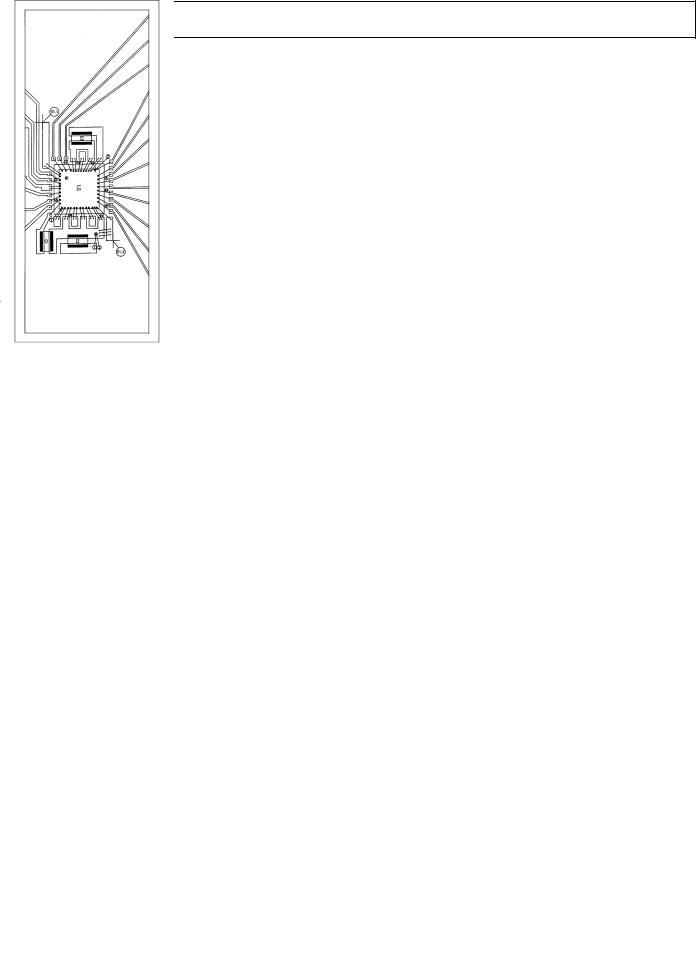
DIE LAYOUT AND MECHANICAL INFORMATION
Die Dimensions . . . . . . . . . . . . . . . . 155 × 168 × 21 (±1) mils Pad Dimensions . . . . . . . . . . . . . . . . . . . . . . . . . . . . 4 × 4 mils Metalization . . . . . . . . . . . . . . . . . . . . . . . . . . . . . . Aluminum Backing . . . . . . . . . . . . . . . . . . . . . . . . . . . . . . . . . . . . . None Substrate Potential . . . . . . . . . . . . . . . . . . . . . . . . . . . . GND Transistor Count . . . . . . . . . . . . . . . . . . . . . . . . . . . . . . 2,605 Passivation . . . . . . . . . . . . . . . . . . . . . . . . . . . . . . . Oxynitride Die Attach . . . . . . . . . . . . . . . . . . . . . . . . . . . . . . Silver Filled Bond Wire . . . . . . . . . . . . . . . . . . . . . . . . . . . . . . . . . . . Gold
DIE LAYOUT W/PAD LABELS
DEFINITION OF SPECIFICATIONS Analog Bandwidth
The analog input frequency at which the spectral power of the fundamental frequency (as determined by the FFT analysis) is reduced by 3 dB.
Aperture Delay
The delay between the 50% point of the rising edge of the ENCODE command and the instant at which the analog input is sampled.
Aperture Uncertainty (Jitter)
The sample-to-sample variation in aperture delay.
Differential Nonlinearity
The deviation of any code from an ideal 1 LSB step.
Encode Pulse Width/Duty Cycle
Pulse width high is the minimum amount of time that the ENCODE pulse should be left in logic “1” state to achieve rated performance; pulse width low is the minimum time ENCODE pulse should be left in low state. At a given clock rate, these specs define an acceptable Encode duty cycle.
Harmonic Distortion
The ratio of the rms signal amplitude to the rms value of the worst harmonic component, reported in dBc.
Integral Nonlinearity
The deviation of the transfer function from a reference line measured in fractions of 1 LSB using a “best straight line” determined by a least square curve fit.
Minimum Conversion Rate
The encode rate at which the SNR of the lowest analog signal frequency drops by no more than 3 dB below the guaranteed limit.
Maximum Conversion Rate
The encode rate at which parametric testing is performed.
Output Propagation Delay
The delay between the 50% point of the rising edge of ENCODE command and the time when all output data bits are within valid logic levels.
Overvoltage Recovery Time
The amount of time required for the converter to recover to 0.02% accuracy after an analog input signal 150% of full scale is reduced to midscale.
Power Supply Rejection Ratio
The ratio of a change in input offset voltage to a change in power supply voltage.
Signal-to-Noise-and-Distortion (SINAD)
The ratio of the rms signal amplitude (set at 1 dB below full scale) to the rms value of the sum of all other spectral components, including harmonics but excluding dc.
Signal-to-Noise Ratio (without Harmonics)
The ratio of the rms signal amplitude (set at 1 dB below full scale) to the rms value of the sum of all other spectral components, excluding the first five harmonics and dc.
Spurious-Free Dynamic Range
The ratio of the rms signal amplitude to the rms value of the peak spurious spectral component. The peak spurious component may or may not be a harmonic. May be reported in dBc (i.e., degrades as signal levels is lowered), or in dBFS (always related back to converter full scale).
Transient Response
The time required for the converter to achieve 0.02% accuracy when a one-half full-scale step function is applied to the analog input.
Two-Tone Intermodulation Distortion Rejection
The ratio of the rms value of either input tone to the rms value of the worst third order intermodulation product; reported in dBc.
Two-Tone SFDR
The ratio of the rms value of either input tone to the rms value of the peak spurious component. The peak spurious component may or may not be an IMD product. May be reported in dBc (i.e., degrades as signal levels is lowered), or in dBFS (always related back to converter full scale).
–6– |
REV. A |

Equivalent Circuits–AD9042
|
|
|
N |
|
|
|
tA = –250 PS TYP |
|
|
||
|
ANALOG |
|
|
|
|
|
INPUT |
N + 1 |
|
|
|
|
|
(AIN) |
|
|
|
|
|
|
|
|
|
|
ENCODE |
|
|
|
|
|
INPUTS |
|
|
|
|
|
(ENCODE) |
|
|
|
|
|
DIGITAL |
|
|
|
|
|
OUTPUTS |
N – 2 |
N – 1 |
N |
|
|
(D11–D0) |
|
|
|
|
|
|
|
tOD = 9ns TYP |
|
|
|
|
|
Figure 1. Timing Diagram |
|
|
AVCC |
|
|
|
|
DVCC |
+3.5V |
|
|
|
|
|
|
|
|
|
|
CURRENT |
|
|
|
|
|
MIRROR |
AVCC |
|
|
|
|
|
250µA |
|
|
250Ω |
|
|
|
|
|
|
|
|
|
250Ω |
|
|
|
|
AIN |
|
|
|
|
|
AVCC |
V |
OFFSET |
|
|
DV |
|
|
|
|
CC |
|
250µA |
VREF |
|
200Ω |
||
D0–D11 |
||
+1.5V |
||
6pF |
||
|
||
Figure 2. Analog Input Stage |
|
|
|
CURRENT |
|
AVCC |
MIRROR |
|
|
AVCC |
|
|
R1 |
AVCC |
Figure 5. Digital Output Stage |
||||
R1 |
|
|
|
||||||
17kΩ |
|
|
17kΩ |
|
|
|
|
|
|
ENCODE |
|
|
|
|
ENCODE |
|
AVCC |
|
|
R2 |
TIMING |
|
R2 |
|
|
|
AVCC |
|
|
|
|
|
|
|
|
||||
CIRCUITS |
|
|
|
|
|
|
|||
8kΩ |
|
8kΩ |
|
|
|
|
|
|
|
|
|
|
|
|
2.4V |
|
|
|
|
|
|
|
|
|
|
|
|
|
VREF |
Figure 3. Encode Inputs |
|
|
|
0.5mA |
|
|
|||
|
|
|
|
|
|
||||
AVCC |
|
|
|
|
Figure 6. 2.4 V Reference |
||||
|
|
|
|
|
|
|
+5V |
|
+5V |
VREF |
AVCC |
|
|
|
|
|
2,12,14 |
|
|
|
AVCC |
|
|
0.1µF |
|
28 |
10kΩ |
||
|
|
|
|
|
200kHz |
8 |
AIN |
|
|
|
|
|
|
|
D11 |
|
|||
|
|
|
|
|
SINEWAVE |
|
|
|
|
|
|
|
|
|
49.9Ω |
9 |
VOFFSET |
|
|
CURRENT |
|
|
|
|
10 |
|
|
|
|
|
|
|
|
|
VREF |
|
|
||
MIRROR |
|
|
|
|
|
|
|
|
|
|
C1 |
|
|
|
TTL CLOCK OSC. |
4 |
ENCODE |
|
|
|
(PIN 10*) |
|
|
|
|
5 |
|
|
|
*AD9042AST ONLY |
|
|
|
|
NC |
ENCODE |
D0 17 |
|
|
INTERNAL NODE ON AD9042AD |
|
|
|
|
|
||||
|
|
|
|
|
|
|
|||
|
|
|
|
|
|
|
1,3,6,7,11,13 |
|
|
Figure 4. Compensation Pin, C1
NOTE: ALL +5V SUPPLY PINS & VREF PIN BYPASSED TO GND
WITH A 0.1µF CAPACITOR. PINS 15,16 ARE NOT CONNECTED.
Figure 7. AD9042AD Burn-In Diagram
REV. A |
–7– |

AD9042–Typical Performance Characteristics
|
0 |
|
|
|
|
|
|
|
|
|
dB |
|
|
|
|
|
|
|
ENCODE = 41 MSPS |
|
|
|
|
|
|
|
|
|
AIN = 1.2MHz |
|
||
– |
|
|
|
|
|
|
|
|
||
–20 |
|
|
|
|
|
|
|
|
|
|
SCALE |
|
|
|
|
|
|
|
|
|
|
–60 |
|
|
|
|
|
|
|
|
|
|
ADCFULL |
|
|
|
|
|
|
|
|
|
|
|
–40 |
|
|
|
|
|
|
|
|
|
TO |
2 |
3 |
4 |
5 |
6 |
7 |
8 |
9 |
|
|
RELATIVE |
|
|
||||||||
–80 |
|
|
|
|
|
|
|
|
|
|
|
|
|
|
|
|
|
|
|
|
|
POWER |
–100 |
|
|
|
|
|
|
|
|
|
–120 |
|
|
|
|
|
|
|
|
|
|
|
|
|
|
|
8.2 |
|
12.3 |
16.4 |
|
|
|
dc |
4.1 |
|
|
|
|
20.5 |
|||
|
|
|
|
|
FREQUENCY – MHz |
|
|
|||
WORST CASE HARMONIC – dBc
|
|
|
|
|
|
|
|
|
|
|
|
|
|
81 |
|
|
|
|
|
|
ENCODE = 41 MSPS |
|
|||||
|
|
|
|
|
|
TEMP = –40°C, +25°C, & +85°C |
|
||||||
80 |
|
|
T = +25°C |
|
|
|
|||||||
|
|
|
|||||||||||
|
|
|
|
|
|
|
|
|
|
|
|
|
|
|
|
T = –40°C |
|
|
|
|
|
|
|
|
|||
|
|
|
|
||||||||||
|
|
|
|
|
|
|
|
|
|
|
|
|
|
|
|
|
|
|
|
|
|
|
|
|
|
|
|
79 |
|
|
T = +85°C |
|
|||||||||
|
|
|
|
|
|
|
|
|
|
|
|
|
|
|
|
|
|
|
|
|
|
|
|
|
|
|
|
78 |
|
|
|
|
|
|
|
|
|
|
|
|
|
|
|
|
|
|
|
|
|
|
|
|
|
|
|
|
|
|
|
|
|
|
|
|
|
|
|
|
|
77
0 |
2 |
4 |
6 |
8 |
10 |
12 |
14 |
16 |
18 |
20 |
|
|
|
ANALOG INPUT FREQUENCY – MHz |
|
|
|||||
Figure 8. Single Tone at 1.2 MHz |
Figure 11. Harmonics vs. AIN |
POWER RELATIVE TO ADC FULL SCALE – dB
0
–20
–40
–60
–80
–100
–120 dc
|
|
|
ENCODE = 41 MSPS |
|
70 |
|
|
|
|
ENCODE = 41 MSPS |
|
|
||||||
|
|
|
AIN = 9.6MHz |
|
|
|
|
|
|
TEMP = –40°C, +25°C, & +85°C |
|
|||||||
|
|
|
|
|
|
|
|
|
|
|
||||||||
|
|
|
|
|
|
|
|
69 |
|
|
|
|
|
|
|
|
|
|
|
|
|
|
|
|
|
|
– dB |
|
T = –40°C |
|
|
|
|
|
|
|
|
|
|
|
|
|
|
|
|
|
|
|
|
|
|
|
|
|
|
|
|
|
|
|
|
|
|
|
68 |
|
|
|
|
|
|
|
|
|
|
4 |
8 8 |
5 |
3 |
7 |
6 |
2 |
|
SNR |
|
|
|
|
|
|
|
T = +25°C |
|
|
|
|
|
|
|
|
|
|
|
|
|
|
|
|
|
|
|
||
|
|
|
|
|
|
|
|
67 |
|
|
T = +85°C |
|
|
|
|
|
|
|
|
|
|
|
|
|
|
|
66 |
|
|
|
|
|
|
|
|
|
|
|
4.1 |
8.2 |
12.3 |
|
16.4 |
|
20.5 |
0 |
2 |
4 |
6 |
8 |
10 |
12 |
14 |
16 |
18 |
20 |
|
|
|
|
|
|
ANALOG INPUT FREQUENCY – MHz |
|
|
||||||||||
|
|
FREQUENCY – MHz |
|
|
|
|
|
|
|
|
|
|||||||
Figure 9. Single Tone at 9.6 MHz |
Figure 12. Noise vs. AIN |
|
0 |
|
|
|
|
|
|
|
|
– dB |
–20 |
ENCODE = 41 MSPS |
|
|
|
|
|
||
SCALE |
AIN = 19.5MHz |
|
|
|
|
|
|
||
FULLADC |
|
|
|
|
|
|
|
||
–60 |
|
|
|
|
|
|
|
|
|
|
–40 |
|
|
|
|
|
|
|
|
TO |
|
2 |
4 |
6 |
8 |
9 |
7 |
5 |
3 |
RELATIVE |
–80 |
|
|
|
|
|
|
|
|
|
|
|
|
|
|
|
|
|
|
POWER |
–100 |
|
|
|
|
|
|
|
|
–120 |
|
|
|
|
|
|
|
|
|
|
|
|
|
8.2 |
12.3 |
|
16.4 |
|
|
|
dc |
|
4.1 |
|
|
20.5 |
|||
FREQUENCY – MHz
Figure 10. Single Tone at 19.5 MHz
|
90 |
|
|
|
|
|
|
|
|
|
|
|
|
|
|
|
|
|
|
|
|
|
|
|
|
|
|
|
|
|
|
|
|
|
|
|
|
|
|
|
|
|
|
|
|
ENCODE = 41 MSPS |
|
|
|
||||
– dBc |
80 |
|
|
|
|
|
|
|
|
|
|
|
|
|
|
|
|
|
|
|
|
|
|
|
|
|
|
|
|
|
|
|
|
||
70 |
|
|
|
|
|
|
|
|
|
|
|
|
|
|
|
|
|
|
|
|
|
|
|
|
|
|
|
|
|
|
|
|
|
||
HARMONIC |
60 |
|
|
|
|
|
|
|
|
|
|
|
|
|
|
|
|
WORST |
50 |
|
|
|
|
|
|
|
|
|
|
|
|
|
|
|
|
|
|
|
|
|
|
|
|
|
|
|
|
|
|
|
|
|
|
|
40 |
|
|
|
|
|
|
|
|
|
|
|
|
|
|
|
|
|
|
|
|
|
|
|
|
|
|
|
|
|
|
|
|
|
|
|
30 |
|
|
|
|
|
|
|
|
|
|
|
|
|
|
|
|
|
|
2 |
4 |
10 |
20 |
40 |
|
|
100 |
||||||||
|
1 |
|
|
||||||||||||||
ANALOG INPUT FREQUENCY – MHz
Figure 13. Harmonics vs. AIN
–8– |
REV. A |
Loading...