


Analog Devices AD9223ARS, AD9223AR, AD9221SSOPEB, AD9221SIOCEB, AD9221ARS Datasheet
...a |
Complete 12-Bit 1.5/3.0/10.0 MSPS |
|
Monolithic A/D Converters |
||
|
|
AD9221/AD9223/AD9220 |
FEATURES
Monolithic 12-Bit A/D Converter Product Family
Family Members Are: AD9221, AD9223, and AD9220
Flexible Sampling Rates: 1.5 MSPS, 3.0 MSPS and
10.0 MSPS
Low Power Dissipation: 59 mW, 100 mW and 250 mW
Single +5 V Supply
Integral Nonlinearity Error: 0.5 LSB
Differential Nonlinearity Error: 0.3 LSB
Input Referred Noise: 0.09 LSB
Complete: On-Chip Sample-and-Hold Amplifier and
Voltage Reference
Signal-to-Noise and Distortion Ratio: 70 dB
Spurious-Free Dynamic Range: 86 dB
Out-of-Range Indicator
Straight Binary Output Data
28-Lead SOIC and 28-Lead SSOP
PRODUCT DESCRIPTION
The AD9221, AD9223, and AD9220 are a generation of high performance, single supply 12-bit analog-to-digital converters. Each device exhibits true 12-bit linearity and temperature drift performance1 as well as 11.5 bit or better ac performance.2 The AD9221/AD9223/AD9220 share the same interface options, package, and pinout. Thus, the product family provides an upward or downward component selection path based on performance, sample rate and power. The devices differ with respect to their specified sampling rate and power consumption which is reflected in their dynamic performance over frequency.
The AD9221/AD9223/AD9220 combine a low cost, high speed CMOS process and a novel architecture to achieve the resolution and speed of existing hybrid and monolithic implementations at a fraction of the power consumption and cost. Each device is a complete, monolithic ADC with an on-chip, high performance, low noise sample-and-hold amplifier and programmable voltage reference. An external reference can also be chosen to suit the dc accuracy and temperature drift requirements of the application.
The devices use a multistage differential pipelined architecture with digital output error correction logic to provide 12-bit accuracy at the specified data rates and to guarantee no missing codes over the full operating temperature range.
The input of the AD9221/AD9223/AD9220 is highly flexible, allowing for easy interfacing to imaging, communications, medical, and data-acquisition systems. A truly differential input structure allows for both single-ended and differential input interfaces of varying input spans. The sample-and-hold (SHA) amplifier is equally suited for both multiplexed systems that switch full-scale voltage levels in successive channels as well as sampling single-channel inputs at frequencies up to and beyond the Nyquist rate. Also, the AD9221/AD9223/AD9220 is well
FUNCTIONAL BLOCK DIAGRAM
|
CLK |
AVDD |
DVDD |
|
|
SHA |
|
|
|
|
|
VINA |
MDAC1 |
MDAC2 |
MDAC3 |
|
|
VINB |
GAIN = 16 |
GAIN = 8 |
GAIN = 4 |
|
|
|
|
|
|
|
|
|
5 |
4 |
3 |
|
A/D |
|
A/D |
A/D |
A/D |
|
|
CAPT |
5 |
4 |
3 |
|
3 |
|
|
||||
CAPB |
DIGITAL CORRECTION LOGIC |
|
|
||
VREF |
|
|
12 |
|
|
|
OUTPUT BUFFERS |
|
OTR |
||
|
|
|
|||
SENSE |
|
|
|
|
BIT 1 |
MODE |
1V |
AD9221/AD9223/AD9220 |
(MSB) |
||
SELECT |
BIT 12 |
||||
|
|
|
|
|
(LSB) |
|
REFCOM |
AVSS |
DVSS |
CML |
|
suited for communication systems employing Direct-IF Down Conversion since the SHA in the differential input mode can achieve excellent dynamic performance far beyond its specified Nyquist frequency.2
A single clock input is used to control all internal conversion cycles. The digital output data is presented in straight binary output format. An out-of-range (OTR) signal indicates an overflow condition which can be used with the most significant bit to determine low or high overflow.
PRODUCT HIGHLIGHTS
The AD9221/AD9223/AD9220 family offers a complete singlechip sampling 12-bit, analog-to-digital conversion function in pin-compatible 28-lead SOIC and SSOP packages.
Flexible Sampling Rates—The AD9221, AD9223 and AD9220 offer sampling rates of 1.5 MSPS, 3.0 MSPS and 10.0 MSPS, respectively.
Low Power and Single Supply—The AD9221, AD9223 and AD9220 consume only 59 mW, 100 mW and 250 mW, respectively, on a single +5 V power supply.
Excellent DC Performance Over Temperature—The AD9221/ AD9223/AD9220 provide 12-bit linearity and temperature drift performance.1
Excellent AC Performance and Low Noise—The AD9221/ AD9223/AD9220 provides better than 11.3 ENOB performance and has an input referred noise of 0.09 LSB rms.2
Flexible Analog Input Range—The versatile onboard sample- and-hold (SHA) can be configured for either single ended or differential inputs of varying input spans.
NOTES
1Excluding internal voltage reference.
2Depends on the analog input configuration.
REV. C
Information furnished by Analog Devices is believed to be accurate and reliable. However, no responsibility is assumed by Analog Devices for its use, nor for any infringements of patents or other rights of third parties which may result from its use. No license is granted by implication or otherwise under any patent or patent rights of Analog Devices.
One Technology Way, P.O. Box 9106, Norwood, MA 02062-9106, U.S.A.
Tel: 781/329-4700 |
World Wide Web Site: http://www.analog.com |
Fax: 781/326-8703 |
© Analog Devices, Inc., 1999 |
AD9221/AD9223/AD9220–SPECIFICATIONS
(AVDD = +5 V, DVDD = +5 V, fSAMPLE = Max Conversion Rate, VREF = 2.5 V, VINB = 2.5 V, TMIN to TMAX unless |
|||||
DC SPECIFICATIONS otherwise noted) |
|
|
|
|
|
Parameter |
|
AD9221 |
AD9223 |
AD9220 |
Units |
|
|
|
|
|
|
RESOLUTION |
|
12 |
12 |
12 |
Bits min |
|
|
|
|
|
|
MAX CONVERSION RATE |
|
1.5 |
3 |
10 |
MHz min |
|
|
|
|
|
|
INPUT REFERRED NOISE (TYP) |
|
|
|
|
|
VREF = 1 V |
|
0.23 |
0.23 |
0.23 |
LSB rms typ |
VREF = 2.5 V |
|
0.09 |
0.09 |
0.09 |
LSB rms typ |
ACCURACY |
|
± 0.4 |
± 0.5 |
± 0.5 |
|
Integral Nonlinearity (INL) |
|
LSB typ |
|||
|
|
± 1.25 |
± 1.25 |
± 1.25 |
LSB max |
Differential Nonlinearity (DNL) |
|
± 0.3 |
± 0.3 |
± 0.3 |
LSB typ |
|
|
± 0.75 |
± 0.75 |
± 0.75 |
LSB max |
INL1 |
|
± 0.6 |
± 0.6 |
± 0.7 |
LSB typ |
DNL1 |
|
± 0.3 |
± 0.3 |
± 0.35 |
LSB typ |
No Missing Codes |
|
12 |
12 |
12 |
Bits Guaranteed |
Zero Error (@ +25°C) |
|
± 0.3 |
± 0.3 |
± 0.3 |
% FSR max |
Gain Error (@ +25°C)2 |
|
± 1.5 |
± 1.5 |
± 1.5 |
% FSR max |
Gain Error (@ +25°C)3 |
|
± 0.75 |
± 0.75 |
± 0.75 |
% FSR max |
TEMPERATURE DRIFT |
|
± 2 |
± 2 |
± 2 |
ppm/°C typ |
Zero Error |
|
||||
Gain Error2 |
|
± 26 |
± 26 |
± 26 |
ppm/°C typ |
Gain Error3 |
|
± 0.4 |
± 0.4 |
± 0.4 |
ppm/°C typ |
POWER SUPPLY REJECTION |
|
|
|
|
|
AVDD, DVDD (+5 V ± 0.25 V) |
|
± 0.06 |
± 0.06 |
± 0.06 |
% FSR max |
ANALOG INPUT |
|
|
|
|
|
Input Span (with VREF = 1.0 V) |
|
2 |
2 |
2 |
V p-p min |
(with VREF = 2.5 V) |
|
5 |
5 |
5 |
V p-p max |
Input (VINA or VINB) Range |
|
0 |
0 |
0 |
V min |
|
|
AVDD |
AVDD |
AVDD |
V max |
Input Capacitance |
|
16 |
16 |
16 |
pF typ |
|
|
|
|
|
|
INTERNAL VOLTAGE REFERENCE |
|
|
|
|
|
Output Voltage (1 V Mode) |
|
1 |
1 |
1 |
Volts typ |
Output Voltage Tolerance (1 V Mode) |
|
± 14 |
± 14 |
± 14 |
mV max |
Output Voltage (2.5 V Mode) |
|
2.5 |
2.5 |
2.5 |
Volts typ |
Output Voltage Tolerance (2.5 V Mode) |
|
± 35 |
± 35 |
± 35 |
mV max |
Load Regulation4 |
|
2.0 |
2.0 |
1.5 |
mV max |
REFERENCE INPUT RESISTANCE |
|
5 |
5 |
5 |
kΩ typ |
|
|
|
|
|
|
POWER SUPPLIES |
|
|
|
|
|
Supply Voltages |
|
|
|
|
V (± 5% AVDD Operating) |
AVDD |
|
+5 |
+5 |
+5 |
|
DVDD |
|
+2.7 to +5.25 |
+2.7 to +5.25 |
+5 (± 5%) |
V |
Supply Current |
|
|
|
|
|
IAVDD |
|
14.0 |
26 |
58 |
mA max |
|
|
11.8 |
20 |
48 |
mA typ |
IDVDD |
|
0.5 |
0.5 |
12 |
mA max |
|
|
0.02 |
0.02 |
10 |
mA typ |
|
|
|
|
|
|
POWER CONSUMPTION |
|
59.0 |
100 |
250 |
mW typ |
|
|
70.0 |
130 |
310 |
mW max |
|
|
|
|
|
|
NOTES
1VREF =1 V.
2Including internal reference.
3Excluding internal reference.
4Load regulation with 1 mA load current (in addition to that required by the AD9220/AD9221/AD9223).
Specification subject to change without notice.
–2– |
REV. C |
AD9221/AD9223/AD9220
(AVDD = +5 V, DVDD= +5 V, fSAMPLE = Max Conversion Rate, VREF = 1.0 V, VINB = 2.5 V, DC Coupled/Single- |
|||||
AC SPECIFICATIONS Ended Input TMIN to TMAX unless otherwise noted) |
|
|
|
||
Parameters |
AD9221 |
|
AD9223 |
AD9220 |
Units |
|
|
|
|
|
|
MAX CONVERSION RATE |
1.5 |
|
3.0 |
10.0 |
MHz min |
|
|
|
|
|
|
DYNAMIC PERFORMANCE |
|
|
|
|
|
Input Test Frequency 1 (VINA = –0.5 dBFS) |
100 |
|
500 |
1000 |
kHz |
Signal-to-Noise and Distortion (SINAD) |
70.0 |
|
70.0 |
70 |
dB typ |
|
69.0 |
|
68.5 |
68.5 |
dB min |
Effective Number of Bits (ENOBs) |
11.3 |
|
11.3 |
11.3 |
dB typ |
|
11.2 |
|
11.1 |
11.1 |
dB min |
Signal-to-Noise Ratio (SNR) |
70.2 |
|
70.0 |
70.2 |
dB typ |
|
69.0 |
|
68.5 |
69.0 |
dB min |
Total Harmonic Distortion (THD) |
–83.4 |
|
–83.4 |
–83.7 |
dB typ |
|
–77.5 |
|
–76.0 |
–76.0 |
dB max |
Spurious Free Dynamic Range (SFDR) |
86.0 |
|
87.5 |
88.0 |
dB typ |
|
79.0 |
|
77.5 |
77.5 |
dB max |
Input Test Frequency 2 (VINA = –0.5 dBFS) |
0.50 |
|
1.50 |
5.0 |
MHz |
Signal-to-Noise and Distortion (SINAD) |
69.9 |
|
69.4 |
67.0 |
dB typ |
|
69.0 |
|
68.0 |
65.0 |
dB min |
Effective Number of Bits (ENOBs) |
11.3 |
|
11.2 |
10.8 |
dB typ |
|
11.2 |
|
11.1 |
10.5 |
dB min |
Signal-to-Noise Ratio (SNR) |
70.1 |
|
69.7 |
68.8 |
dB typ |
|
69.0 |
|
68.5 |
67.5 |
dB min |
Total Harmonic Distortion (THD) |
–83.4 |
|
–82.9 |
–72.0 |
dB typ |
|
–77.5 |
|
–75.0 |
–68.0 |
dB max |
Spurious Free Dynamic Range (SFDR) |
86.0 |
|
85.7 |
75.0 |
dB typ |
|
79.0 |
|
76.0 |
69.0 |
dB max |
Full Power Bandwidth |
25 |
|
40 |
60 |
MHz typ |
Small Signal Bandwidth |
25 |
|
40 |
60 |
MHz typ |
Aperture Delay |
1 |
|
1 |
1 |
ns typ |
Aperture Jitter |
4 |
|
4 |
4 |
ps rms typ |
Acquisition to Full-Scale Step |
125 |
|
43 |
30 |
ns typ |
|
|
|
|
|
|
Specifications subject to change without notice.
DIGITAL SPECIFICATIONS (AVDD = +5 V, DVDD = +5 V, TMIN to TMAX unless otherwise noted)
Parameters |
Symbol |
|
Units |
|
|
|
|
CLOCK INPUT |
|
|
|
High Level Input Voltage |
VIH |
+3.5 |
V min |
Low Level Input Voltage |
VIL |
+1.0 |
V max |
High Level Input Current (VIN = DVDD) |
IIH |
±10 |
A max |
Low Level Input Current (VIN = 0 V) |
IIL |
±10 |
A max |
Input Capacitance |
CIN |
5 |
pF typ |
LOGIC OUTPUTS |
|
|
|
DVDD = 5 V |
|
|
|
High Level Output Voltage (IOH = 50 A) |
VOH |
+4.5 |
V min |
High Level Output Voltage (IOH = 0.5 mA) |
VOH |
+2.4 |
V min |
Low Level Output Voltage (IOL = 1.6 mA) |
VOL |
+0.4 |
V max |
Low Level Output Voltage (IOL = 50 A) |
VOL |
+0.1 |
V max |
DVDD = 3 V |
|
|
|
High Level Output Voltage (IOH = 50 A) |
VOH |
+2.95 |
V min |
High Level Output Voltage (IOH = 0.5 mA) |
VOH |
+2.80 |
V min |
Low Level Output Voltage (IOL = 1.6 mA) |
VOL |
+0.4 |
V max |
Low Level Output Voltage (IOL = 50 A) |
VOL |
+0.05 |
V max |
Output Capacitance |
COUT |
5 |
pF typ |
Specifications subject to change without notice.
REV. C |
–3– |
AD9221/AD9223/AD9220
SWITCHING SPECIFICATIONS (TMIN to TMAX with AVDD = +5 V, DVDD = +5 V, CL = 20 pF)
Parameters |
Symbol |
AD9221 |
AD9223 |
AD9220 |
Units |
|
|
|
|
|
|
Clock Period1 |
tC |
667 |
333 |
100 |
ns min |
CLOCK Pulsewidth High |
tCH |
300 |
150 |
45 |
ns min |
CLOCK Pulsewidth Low |
tCL |
300 |
150 |
45 |
ns min |
Output Delay |
tOD |
8 |
8 |
8 |
ns min |
|
|
13 |
13 |
13 |
ns typ |
|
|
19 |
19 |
19 |
ns max |
Pipeline Delay (Latency) |
|
3 |
3 |
3 |
Clock Cycles |
|
|
|
|
|
|
NOTES
1The clock period may be extended to 1 ms without degradation in specified performance @ +25 °C.
Specifications subject to change without notice.
|
S1 |
|
S2 |
ANALOG |
|
tC |
S4 |
INPUT |
tCH |
S3 |
|
|
|
tCL |
|
INPUT |
|
|
|
CLOCK |
|
|
|
|
|
|
tOD |
DATA |
|
|
DATA 1 |
OUTPUT |
|
|
|
|
|
|
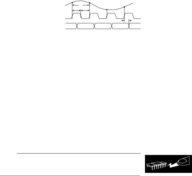
Figure 1. Timing Diagram
ABSOLUTE MAXIMUM RATINGS*
|
With |
|
|
|
|
Respect |
|
|
|
Parameter |
to |
Min |
Max |
Units |
|
|
|
|
|
AVDD |
AVSS |
–0.3 |
+6.5 |
V |
DVDD |
DVSS |
–0.3 |
+6.5 |
V |
AVSS |
DVSS |
–0.3 |
+0.3 |
V |
AVDD |
DVDD |
–6.5 |
+6.5 |
V |
REFCOM |
AVSS |
–0.3 |
+0.3 |
V |
CLK |
AVSS |
–0.3 |
AVDD + 0.3 |
V |
Digital Outputs |
DVSS |
–0.3 |
DVDD + 0.3 |
V |
VINA, VINB |
AVSS |
–0.3 |
AVDD + 0.3 |
V |
VREF |
AVSS |
–0.3 |
AVDD + 0.3 |
V |
SENSE |
AVSS |
–0.3 |
AVDD + 0.3 |
V |
CAPB, CAPT |
AVSS |
–0.3 |
AVDD + 0.3 |
V |
Junction Temperature |
|
|
+150 |
°C |
Storage Temperature |
|
–65 |
+150 |
°C |
Lead Temperature |
|
|
|
°C |
(10 sec) |
|
|
+300 |
|
|
|
|
|
|
*Stresses above those listed under Absolute Maximum Ratings may cause permanent damage to the device. This is a stress rating only; functional operation of the device at these or any other conditions above those indicated in the operational sections of this specification is not implied. Exposure to absolute maximum ratings for extended periods may effect device reliability.
THERMAL CHARACTERISTICS
Thermal Resistance 28-Lead SOIC
θJA = 71.4°C/W
θJC = 23°C/W 28-Lead SSOP
θJA = 63.3°C/W
θJC = 23°C/W
ORDERING GUIDE
|
Temperature |
Package |
|
Package |
Model |
Range |
Description |
|
Options |
|
|
|
|
|
AD9221AR |
–40°C to +85°C |
28-Lead SOIC |
|
R-28 |
AD9223AR |
–40°C to +85°C |
28-Lead SOIC |
|
R-28 |
AD9220AR |
–40°C to +85°C |
28-Lead SOIC |
|
R-28 |
AD9221ARS |
–40°C to +85°C |
28-Lead SSOP |
|
RS-28 |
AD9223ARS |
–40°C to +85°C |
28-Lead SSOP |
|
RS-28 |
AD9220ARS |
–40°C to +85°C |
28-Lead SSOP |
|
RS-28 |
AD9220/AD9221/AD9223SOICEB |
Evaluation Board |
|
||
AD9220/AD9221/AD9223SSOPEB |
Evaluation Board |
|
||
|
|
|
|
|
CAUTION
ESD (electrostatic discharge) sensitive device. Electrostatic charges as high as 4000 V readily accumulate on the human body and test equipment and can discharge without detection. Although these devices feature proprietary ESD protection circuitry, permanent damage may occur on devices subjected to high energy electrostatic discharges. Therefore, proper ESD precautions are recommended to avoid performance degradation or loss of functionality.
WARNING!
ESD SENSITIVE DEVICE
–4– |
REV. C |

AD9221/AD9223/AD9220
PIN CONNECTIONS
CLK |
|
|
|
DVDD |
1 |
|
28 |
||
(LSB) BIT 12 |
|
|
|
DVSS |
2 |
|
27 |
||
BIT 11 |
|
|
|
|
3 |
|
26 |
AVDD |
|
BIT 10 |
|
|
|
AVSS |
4 |
AD9221/ |
25 |
||
BIT 9 |
|
|
VINB |
|
5 |
AD9223/ |
24 |
||
BIT 8 |
|
AD9220 |
|
|
6 |
23 |
VINA |
||
BIT 7 |
|
|
|
|
7 |
TOP VIEW |
22 |
CML |
|
|
|
(Not to Scale) |
|
|
BIT 6 |
8 |
21 |
CAPT |
|
BIT 5 |
|
|
|
|
9 |
|
20 |
CAPB |
|
|
|
|
|
|
BIT 4 |
10 |
|
19 |
REFCOM |
|
|
|
|
|
BIT 3 |
11 |
|
18 |
VREF |
|
|
|
|
|
BIT 2 |
12 |
|
17 |
SENSE |
|
|
|
|
|
(MSB) BIT 1 |
13 |
|
16 |
AVSS |
|
|
|
|
|
OTR |
14 |
|
15 |
AVDD |
|
|
|
|
|
PIN FUNCTION DESCRIPTIONS
Pin |
|
|
Number |
Name |
Description |
|
|
|
1 |
CLK |
Clock Input Pin |
2 |
BIT 12 |
Least Significant Data Bit (LSB) |
3–12 |
BIT N |
Data Output Bit |
13 |
BIT 1 |
Most Significant Data Bit (MSB) |
14 |
OTR |
Out of Range |
15, 26 |
AVDD |
+5 V Analog Supply |
16, 25 |
AVSS |
Analog Ground |
17 |
SENSE |
Reference Select |
18 |
VREF |
Reference I/O |
19 |
REFCOM |
Reference Common |
20 |
CAPB |
Noise Reduction Pin |
21 |
CAPT |
Noise Reduction Pin |
22 |
CML |
Common-Mode Level (Midsupply) |
23 |
VINA |
Analog Input Pin (+) |
24 |
VINB |
Analog Input Pin (–) |
27 |
DVSS |
Digital Ground |
28 |
DVDD |
+3 V to +5 V Digital Supply |
|
|
|
DEFINITIONS OF SPECIFICATION
INTEGRAL NONLINEARITY (INL)
INL refers to the deviation of each individual code from a line drawn from “negative full scale” through “positive full scale.” The point used as “negative full scale” occurs 1/2 LSB before the first code transition. “Positive full scale” is defined as a level 1 1/2 LSB beyond the last code transition. The deviation is measured from the middle of each particular code to the true straight line.
DIFFERENTIAL NONLINEARITY (DNL, NO MISSING CODES)
An ideal ADC exhibits code transitions that are exactly 1 LSB apart. DNL is the deviation from this ideal value. Guaranteed no missing codes to 12-bit resolution indicates that all 4096 codes, respectively, must be present over all operating ranges.
REV. C
ZERO ERROR
The major carry transition should occur for an analog value 1/2 LSB below VINA = VINB. Zero error is defined as the deviation of the actual transition from that point.
GAIN ERROR
The first code transition should occur at an analog value 1/2 LSB above negative full scale. The last transition should occur at an analog value 1 1/2 LSB below the nominal full scale. Gain error is the deviation of the actual difference between first and last code transitions and the ideal difference between first and last code transitions.
TEMPERATURE DRIFT
The temperature drift for zero error and gain error specifies the maximum change from the initial (+25°C) value to the value at
TMIN or TMAX.
POWER SUPPLY REJECTION
The specification shows the maximum change in full scale from the value with the supply at the minimum limit to the value with the supply at its maximum limit.
APERTURE JITTER
Aperture jitter is the variation in aperture delay for successive samples and is manifested as noise on the input to the A/D.
APERTURE DELAY
Aperture delay is a measure of the sample-and-hold amplifier (SHA) performance and is measured from the rising edge of the clock input to when the input signal is held for conversion.
SIGNAL-TO-NOISE AND DISTORTION (S/N+D, SINAD) RATIO
S/N+D is the ratio of the rms value of the measured input signal to the rms sum of all other spectral components below the Nyquist frequency, including harmonics but excluding dc.
The value for S/N+D is expressed in decibels.
EFFECTIVE NUMBER OF BITS (ENOB)
For a sine wave, SINAD can be expressed in terms of the number of bits. Using the following formula,
N = (SINAD – 1.76)/6.02
it is possible to get a measure of performance expressed as N, the effective number of bits.
Thus, effective number of bits for a device for sine wave inputs at a given input frequency can be calculated directly from its measured SINAD.
TOTAL HARMONIC DISTORTION (THD)
THD is the ratio of the rms sum of the first six harmonic components to the rms value of the measured input signal and is expressed as a percentage or in decibels.
SIGNAL-TO-NOISE RATIO (SNR)
SNR is the ratio of the rms value of the measured input signal to the rms sum of all other spectral components below the Nyquist frequency, excluding the first six harmonics and dc. The value for SNR is expressed in decibels.
SPURIOUS FREE DYNAMIC RANGE (SFDR)
SFDR is the difference in dB between the rms amplitude of the input signal and the peak spurious signal.
–5–
AD9221/AD9223/AD9220
AD9221–Typical Characterization Curves
(AVDD = +5 V, DVDD = +5 V, fSAMPLE = 1.5 MSPS, TA = +258C)
|
1.0 |
|
|
0.8 |
|
|
0.6 |
|
|
0.4 |
|
LSBs |
0.2 |
|
0.0 |
|
|
– |
–0.2 |
|
DNL |
|
|
–0.4 |
|
|
|
|
|
|
–0.6 |
|
|
–0.8 |
|
|
–1.0 |
|
|
0 |
4095 |
|
|
CODE |
|
1.0 |
|
|
|
|
|
0.8 |
|
|
8,180,388 |
|
|
|
|
|
|
|
|
0.6 |
|
|
|
|
|
0.4 |
|
|
|
|
–INLLSBs |
0.2 |
|
HITS |
|
|
0.0 |
|
|
|
||
|
|
|
|
|
|
|
–0.2 |
|
|
|
|
|
–0.4 |
|
|
|
|
|
–0.6 |
|
121,764 |
|
|
|
|
|
|
|
|
|
–0.8 |
|
|
|
85,895 |
|
|
|
|
|
|
|
–1.0 |
|
N–1 |
N |
N+1 |
|
0 |
4095 |
|||
|
|
CODE |
|
CODE |
|
|
|
|
|
|
Figure 2. Typical DNL |
Figure 3. Typical INL |
Figure 4. “Grounded-Input” |
|
|
Histogram (Input Span = 2 V p-p) |
|
80 |
|
|
–50 |
|
|
75 |
|
|
–55 |
|
|
|
|
|
|
|
|
70 |
–0.5dB |
|
–60 |
–20.0dB |
|
|
|
–65 |
|
|
|
|
–6.0dB |
|
|
|
– dB |
65 |
|
–70 |
|
|
|
– dB |
|
|||
|
|
|
|||
60 |
|
–75 |
–6.0dB |
||
SINAD |
|
THD |
|
||
55 |
–20.0dB |
–80 |
|
||
|
50 |
|
–85 |
–0.5dB |
|
|
|
|
|
||
|
|
|
–90 |
|
|
|
|
|
|
|
|
|
45 |
|
|
–95 |
|
|
|
|
|
|
|
|
40 |
|
|
–100 |
|
|
0.1 |
1.0 |
|
0.1 |
1.0 |
|
|
FREQUENCY – MHz |
|
|
FREQUENCY – MHz |
Figure 5. SINAD vs. Input Frequency |
Figure 6. THD vs. Input Frequency |
(Input Span = 2.0 V p-p, VCM = 2.5 V) |
(Input Span = 2.0 V p-p, VCM = 2.5 V) |
|
80 |
|
|
|
75 |
–0.5dB |
|
|
|
|
|
|
70 |
|
|
dB– |
65 |
–6.0dB |
|
|
|
||
SINAD |
60 |
|
|
55 |
–20.0dB |
|
|
|
50 |
|
|
|
45 |
|
|
|
40 |
0.1 |
1.0 |
|
|
||
|
|
FREQUENCY – MHz |
|
Figure 7. SINAD vs. Input Frequency (Input Span = 5.0 V p-p, VCM = 2.5 V)
|
–50 |
|
|
|
–55 |
|
|
|
–60 |
–20.0dB |
|
|
|
||
dB |
–65 |
|
|
|
–0.5dB |
||
THD– |
–70 |
||
|
|||
–75 |
|
||
|
–6.0dB |
||
|
|
||
|
–80 |
|
|
|
–85 |
|
|
|
–90 |
|
|
|
0.1 |
1.0 |
FREQUENCY – MHz
Figure 8. THD vs. Input Frequency (Input Span = 5.0 V p-p, VCM = 2.5 V)
|
–60 |
|
|
|
|
|
|
|
|
–65 |
|
|
|
|
|
|
|
|
–70 |
|
|
|
|
|
|
|
– dB |
–75 |
|
|
|
|
|
|
|
–80 |
|
|
|
|
|
|
|
|
THD |
|
|
|
|
|
5V p-p |
|
|
|
|
|
|
|
|
|
||
–85 |
|
|
|
|
|
|
|
|
|
|
|
|
|
|
|
|
|
|
|
|
|
|
|
|
2V p-p |
|
|
–90 |
|
|
|
|
|
|
|
|
–95 |
|
|
|
|
|
|
|
–100 |
|
|
|
|
|
|
|
|
|
0.2 |
0.3 |
0.4 |
0.6 |
0.8 |
1 |
2 |
3 |
SAMPLE RATE – MSPS
Figure 9. THD vs. Sample Rate
(AIN = –0.5 dB, fIN = 500 kHz, VCM = 2.5 V)
|
100 |
|
|
|
|
|
|
|
90 |
|
|
|
|
|
|
|
80 |
|
|
|
|
|
|
– dB |
70 |
|
|
|
|
|
|
60 |
|
|
SFDR |
|
|
|
|
SNR/SFDR |
|
|
|
|
|
|
|
50 |
|
|
|
|
|
|
|
40 |
|
|
SNR |
|
|
|
|
|
|
|
|
|
|
||
|
|
|
|
|
|
|
|
|
30 |
|
|
|
|
|
|
|
20 |
|
|
|
|
|
|
|
10 |
–50 |
–40 |
–30 |
–20 |
–10 |
0 |
|
–60 |
||||||
|
|
|
|
AI N – dBFS |
|
|
|
Figure 10. SNR/SFDR vs. AIN (Input Amplitude) (fIN = 500 kHz, Input Span = 2 V p-p, VCM = 2.5 V)
–6– |
REV. C |

AD9221/AD9223/AD9220
AD9223–Typical Characterization Curves (AVDD = +5 V, DVDD = +5 V, fSAMPLE = 3.0 MSPS, TA = +258C)
|
1.0 |
|
|
0.8 |
|
|
0.6 |
|
|
0.4 |
|
– LSBs |
0.2 |
|
0.0 |
|
|
DNL |
–0.2 |
|
|
|
|
|
–0.4 |
|
|
–0.6 |
|
|
–0.8 |
|
|
–1.0 |
|
|
0 |
4095 |
|
|
CODE |
|
1.0 |
|
|
|
|
|
0.8 |
|
|
8,123,672 |
|
|
|
|
|
|
|
|
0.6 |
|
|
|
|
|
0.4 |
|
|
|
|
–INLLSBs |
0.2 |
|
HITS |
|
|
0.0 |
|
|
|
||
|
|
|
|
|
|
|
–0.2 |
|
|
|
|
|
–0.4 |
|
|
|
|
|
–0.6 |
|
|
|
130,323 |
|
|
|
96,830 |
|
|
|
–0.8 |
|
|
|
|
|
|
|
|
|
|
|
–1.0 |
|
|
|
|
|
0 |
4095 |
N–1 |
N |
N+1 |
|
|
CODE |
|
CODE |
|
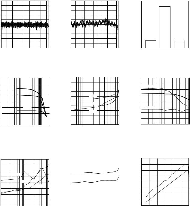
Figure 11. Typical DNL |
Figure 12. Typical INL |
Figure 13. “Grounded-Input” |
|
|
Histogram (Input Span = 2 V p-p) |
|
80 |
|
|
|
75 |
|
|
|
70 |
–0.5dB |
|
|
|
|
|
|
65 |
–6.0dB |
|
– dB |
|
|
|
60 |
|
|
|
SINAD |
|
|
|
55 |
–20.0dB |
|
|
|
|
|
|
|
50 |
|
|
|
45 |
|
|
|
40 |
|
|
|
0.1 |
1.0 |
10.0 |
|
|
FREQUENCY – MHz |
|
|
–50 |
|
|
|
–55 |
|
|
|
–60 |
–20.0dB |
|
|
–65 |
|
|
|
|
|
|
– dB |
–70 |
|
|
–75 |
–0.5dB |
|
|
THD |
|
||
–80 |
–6.0dB |
|
|
|
–85 |
|
|
|
|
|
|
|
–90 |
|
|
|
–95 |
|
|
|
–100 |
|
|
|
0.1 |
1.0 |
10.0 |
|
|
FREQUENCY – MHz |
|
Figure 14. SINAD vs. Input Frequency |
Figure 15. THD vs. Input Frequency |
(Input Span = 2.0 V p-p, VCM = 2.5 V) |
(Input Span = 2.0 V p-p, VCM = 2.5 V) |
|
80 |
|
|
|
75 |
–0.5dB |
|
|
|
|
|
|
70 |
|
|
– dB |
65 |
–6.0dB |
|
60 |
|
|
|
SINAD |
|
|
|
55 |
|
|
|
|
|
|
|
|
50 |
–20.0dB |
|
|
|
|
|
|
45 |
|
|
|
40 |
|
|
|
0.1 |
1.0 |
10.0 |
|
|
FREQUENCY – MHz |
|
Figure 16. SINAD vs. Input Frequency (Input Span = 5.0 V p-p, VCM = 2.5 V)
|
–50 |
|
|
|
–55 |
|
|
|
–60 |
|
|
|
–65 |
–20.0dB |
|
|
|
|
|
– dB |
–70 |
|
|
–75 |
–6.0dB |
|
|
THD |
|
||
|
|
||
–80 |
|
|
|
|
|
|
|
|
–85 |
–0.5dB |
|
|
|
|
|
|
–90 |
|
|
|
–95 |
|
|
|
–100 |
|
|
|
0.1 |
1.0 |
10.0 |
FREQUENCY – MHz
Figure 17. THD vs. Input Frequency (Input Span = 5.0 V p-p, VCM = 2.5 V)
–60
–65
–70
dB |
–75 |
|
|
|
5V p-p |
||
– |
–80 |
||
|
|||
THD |
|
||
–85 |
2V p-p |
||
|
|||
|
|
–90
–95 |
|
|
|
|
|
|
|
|
|
|
|
|
|
|
|
|
|
|
|
|
|
–100 |
|
|
|
|
|
|
|
|
|
|
|
|
|
|
|
|
|
|
|
|
|
0.4 |
0.6 |
0.8 |
1 |
2 |
3 |
4 |
5 |
6 |
||
|
|
|
SAMPLE RATE – MSPS |
|
|
|
|
|||
Figure 18. THD vs. Sample Rate (AIN = –0.5 dB, fIN = 500 kHz, VCM = 2.5 V)
|
100 |
|
|
|
|
|
|
|
90 |
|
|
|
|
|
|
|
80 |
|
|
|
|
|
|
– dB |
70 |
|
|
|
|
|
|
60 |
|
SFDR |
|
|
|
||
SNR/SFDR |
|
|
|
|
|
|
|
50 |
|
|
|
|
|
|
|
40 |
|
|
SNR |
|
|
|
|
|
|
|
|
|
|
||
|
|
|
|
|
|
|
|
|
30 |
|
|
|
|
|
|
|
20 |
|
|
|
|
|
|
|
10 |
|
|
|
|
|
|
|
–60 |
–50 |
–40 |
–30 |
–20 |
–10 |
0 |
AIN – dBFS
Figure 19. SNR/SFDR vs. AIN (Input Amplitude) (fIN = 1.5 MHz, Input Span = 2 V p-p, VCM = 2.5 V)
REV. C |
–7– |
AD9221/AD9223/AD9220
AD9220–Typical Characterization Curves
(AVDD = +5 V, DVDD = +5 V, fSAMPLE = 10 MSPS, TA = +258C)
|
1.0 |
|
|
0.8 |
|
|
0.6 |
|
|
0.4 |
|
LSBs |
0.2 |
|
0.0 |
|
|
– |
|
|
DNL |
–0.2 |
|
–0.4 |
|
|
|
|
|
|
–0.6 |
|
|
–0.8 |
|
|
–1.0 |
|
|
1 |
4095 |
|
|
CODE |
Figure 20. Typical DNL
|
1.0 |
|
|
|
|
|
0.8 |
|
|
8,123,672 |
|
|
|
|
|
|
|
|
0.6 |
|
|
|
|
LSBs–INL |
0.4 |
|
HITS |
|
|
–0.2 |
|
|
|
||
|
0.2 |
|
|
|
|
|
0.0 |
|
|
|
|
|
–0.4 |
|
|
|
|
|
–0.6 |
|
134,613 |
|
130,323 |
|
–0.8 |
|
|
|
|
|
–1.0 |
|
|
|
|
|
1 |
4095 |
N–1 |
N |
N+1 |
|
|
CODE |
|
CODE |
|
|
|
|
|
|
Figure 21. Typical INL |
Figure 22. “Grounded-Input” |
|
Histogram (Input Span = 2 V p-p) |
|
80 |
|
|
|
75 |
–0.5dB |
|
|
|
|
|
|
70 |
|
|
|
|
–6dB |
|
– dB |
65 |
|
|
60 |
|
|
|
SINAD |
|
|
|
55 |
–20dB |
|
|
|
50 |
|
|
|
45 |
|
|
|
40 |
|
|
|
0.1 |
1.0 |
10.0 |
|
|
FREQUENCY – MHz |
|
Figure 23. SINAD vs. Input Frequency (Input Span = 2.0 V p-p, VCM = 2.5 V)
|
–50 |
|
|
|
–55 |
|
|
|
–60 |
|
|
|
|
–20.0dB |
|
– dB |
–65 |
|
|
–70 |
–0.5dB |
|
|
THD |
|
|
|
|
–6.0dB |
|
|
–75 |
|
|
|
|
|
|
|
|
–80 |
|
|
|
–85 |
|
|
|
–90 |
|
|
|
0.1 |
1.0 |
10.0 |
|
|
FREQUENCY – MHz |
|
Figure 26. THD vs. Input Frequency (Input Span = 5.0 V p-p, VCM = 2.5 V)
|
–50 |
|
|
|
80 |
|
|
|
–55 |
|
|
|
75 |
|
|
|
|
|
|
|
–0.5dB |
|
|
|
–60 |
|
|
|
|
|
|
|
|
|
|
|
|
|
|
|
–65 |
|
|
|
70 |
–6.0dB |
|
|
|
|
|
|
|
||
dB |
–70 |
|
–20dB |
dB– |
65 |
|
|
THD– |
|
|
SINAD |
|
|
|
|
–80 |
|
|
60 |
|
|
||
|
–75 |
|
–6dB |
|
|
|
|
|
|
|
|
|
|
|
|
|
|
|
|
|
55 |
–20.0dB |
|
|
–85 |
|
–0.5dB |
|
50 |
|
|
|
–90 |
|
|
|
|
|
|
|
|
|
|
|
|
|
|
|
–95 |
|
|
|
45 |
|
|
|
|
|
|
|
|
|
|
|
–100 |
|
|
|
40 |
|
|
|
0.5 |
1.0 |
10.0 |
|
0.1 |
1.0 |
10.0 |
|
|
|
FREQUENCY – MHz |
|
|
FREQUENCY – MHz |
|
Figure 24. THD vs. Input Frequency |
Figure 25. SINAD vs. Input Fre- |
(Input Span = 2.0 V p-p, VCM = 2.5 V) |
quency (Input Span = 5.0 V p-p, |
|
VCM = 2.5 V) |
|
–60 |
|
|
|
|
|
|
|
|
|
|
|
|
|
|
|
|
|
|
|
|
|
|
|
|
|
|
|
|
|
|
|
|
|
|
|
|
|
|
|
|
|
|
|
|
|
|
|
–65 |
|
|
|
|
|
|
|
|
|
|
|
|
|
|
|
|
|
|
|
|
|
|
|
|
|
|
|
|
|
|
|
|
|
|
|
|
|
|
|
|
|
|
|
|
|
|
|
–70 |
|
|
|
|
|
|
|
5V p-p |
|
|
|
|
|
|
|
|
|
|
|
|||
|
–75 |
|
|
|
|
|
|
|
|
|
|
|
|
|
|
|
|
|
|
|
|
|
|
– dB |
|
|
|
|
|
|
|
2V p-p |
|
|
|
|
|
|
|
|
|
|
|
||||
|
|
|
|
|
|
|
|
|
|
|
|
|
|
|
|
|
|
|
|||||
–80 |
|
|
|
|
|
|
|
|
|
|
|
|
|
|
|
|
|
|
|
|
|
|
|
THD |
|
|
|
|
|
|
|
|
|
|
|
|
|
|
|
|
|
|
|
|
|
|
|
–85 |
|
|
|
|
|
|
|
|
|
|
|
|
|
|
|
|
|
|
|
|
|
|
|
|
|
|
|
|
|
|
|
|
|
|
|
|
|
|
|
|
|
|
|
|
|
|
|
|
|
|
|
|
|
|
|
|
|
|
|
|
|
|
|
|
|
|
|
|
|
|
|
|
–90 |
|
|
|
|
|
|
|
|
|
|
|
|
|
|
|
|
|
|
|
|
|
|
|
|
|
|
|
|
|
|
|
|
|
|
|
|
|
|
|
|
|
|
|
|
|
|
|
–95 |
|
|
|
|
|
|
|
|
|
|
|
|
|
|
|
|
|
|
|
|
|
|
|
|
|
|
|
|
|
|
|
|
|
|
|
|
|
|
|
|
|
|
|
|
|
|
|
–100 |
|
|
|
|
|
|
|
|
|
|
|
|
|
|
|
|
|
|
|
|
|
|
|
|
|
|
|
|
|
|
|
|
|
|
|
|
|
|
|
|
|
|
|
|
|
|
|
1 |
10 |
|
|
15 |
||||||||||||||||||
|
|
|
|
|
|
|
SAMPLE RATE – MSPS |
|
|
|
|||||||||||||
Figure 27. THD vs. Clock Frequency
(AIN = –0.5 dB, fIN = 1.0 MHz, VCM = 2.5 V)
|
90 |
|
|
|
|
|
|
|
80 |
|
|
|
SFDR |
|
|
|
|
|
|
|
|
||
|
70 |
|
|
|
|
|
|
dB |
60 |
|
|
|
|
|
|
– |
|
|
|
|
SNR |
|
|
|
|
|
|
|
|
||
SNR/SFDR |
|
|
|
|
|
|
|
50 |
|
|
|
|
|
|
|
40 |
|
|
|
|
|
|
|
|
|
|
|
|
|
|
|
|
30 |
|
|
|
|
|
|
|
20 |
|
|
|
|
|
|
|
10 |
–50 |
–40 |
–30 |
–20 |
–10 |
0 |
|
–60 |
||||||
AIN – dBFS
Figure 28. SNR/SFDR vs. AIN (Input Amplitude) (fIN = 5.0 MHz, Input Span = 2 V p-p, VCM = 2.5 V)
–8– |
REV. C |
INTRODUCTION
The AD9221/AD9223/AD9220 are members of a high performance, complete single-supply 12-bit ADC product family based on the same CMOS pipelined architecture. The product family allows the system designer an upward or downward component selection path based on dynamic performance, sample rate, and power. The analog input range of the AD9221/AD9223/AD9220 is highly flexible allowing for both single-ended or differential inputs of varying amplitudes which can be ac or dc coupled. Each device shares the same interface options, pinout and package offering.
The AD9221/AD9223/AD9220 utilize a four-stage pipeline architecture with a wideband input sample-and-hold amplifier (SHA) implemented on a cost-effective CMOS process. Each stage of the pipeline, excluding the last stage, consists of a low resolution flash A/D connected to a switched capacitor DAC and interstage residue amplifier (MDAC). The residue amplifier amplifies the difference between the reconstructed DAC output and the flash input for the next stage in the pipeline. One bit of redundancy is used in each of the stages to facilitate digital correction of flash errors. The last stage simply consists of a flash A/D.
The pipeline architecture allows a greater throughput rate at the expense of pipeline delay or latency. This means that while the converter is capable of capturing a new input sample every clock cycle, it actually takes three clock cycles for the conversion to be fully processed and appear at the output. This latency is not a concern in most applications. The digital output, together with the out-of-range indicator (OTR), is latched into an output buffer to drive the output pins. The output drivers of the AD9220ARS, AD9221 and AD9223 can be configured to interface with +5 V or +3.3 V logic families, while the AD9220AR can only be configured for +5 V logic.
The AD9221/AD9223/AD9220 use both edges of the clock in their internal timing circuitry (see Figure 1 and specification page for exact timing requirements). The A/D samples the analog input on the rising edge of the clock input. During the clock low time (between the falling edge and rising edge of the clock), the input SHA is in the sample mode; during the clock high time it is in hold. System disturbances just prior to the rising edge of the clock and/or excessive clock jitter may cause the input SHA to acquire the wrong value, and should be minimized.
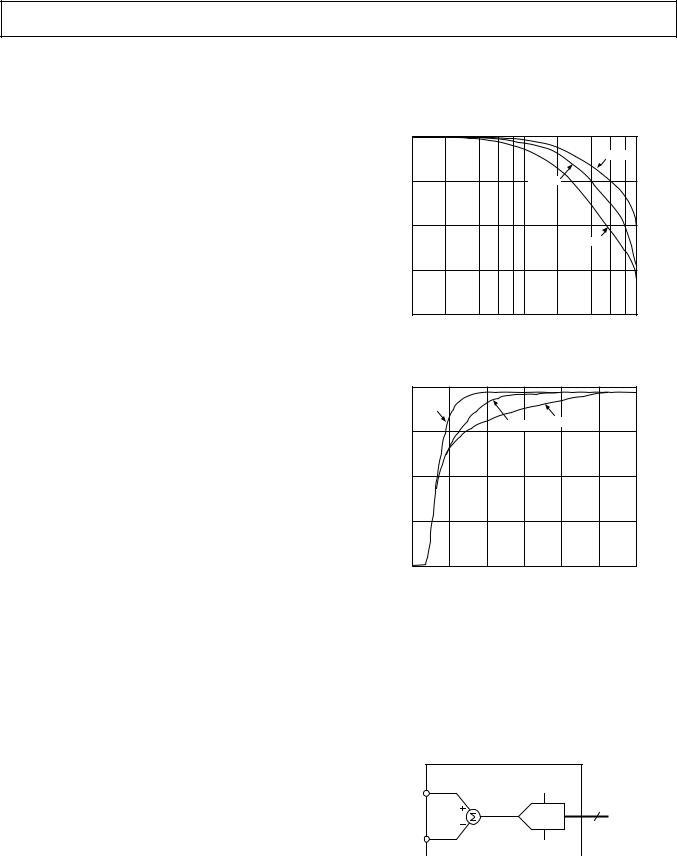
The internal circuitry of both the input SHA and individual pipeline stages of each member of the product family are optimized for both power dissipation and performance. An inherent tradeoff exists between the input SHA’s dynamic performance and its power dissipation. Figures 29 and 30 shows this tradeoff by comparing the full-power bandwidth and settling time of the AD9221/AD9223/AD9220. Both figures reveal that higher full-power bandwidths and faster settling times are achieved at the expense of an increase in power dissipation. Similarly, a tradeoff exists between the sampling rate and the power dissipated in each stage.
As previously stated, the AD9220, AD9221 and AD9223 are similar in most aspects except for the specified sampling rate, power consumption, and dynamic performance. The product family is highly flexible providing several different input ranges
AD9221/AD9223/AD9220
and interface options. As a result, many of the application issues and tradeoffs associated with these resulting configurations are also similar. The data sheet is structured such that the designer can make an informed decision in selecting the proper A/D and optimizing its performance to fit the specific application.
|
0 |
|
|
|
|
|
AD9220 |
|
–3 |
|
AD9223 |
– dB |
|
|
|
AMPLITUDE |
–6 |
|
|
|
|
AD9221 |
|
|
|
|
|
|
–9 |
|
|
–12 |
|
|
|
|
1 |
10 |
100 |
FREQUENCY – MHz
Figure 29. Full-Power Bandwidth
|
4000 |
|
|
|
|
|
|
|
|
AD9220 |
|
|
|
|
|
|
|
|
|
AD9223 |
AD9221 |
|
|
|
3000 |
|
|
|
|
|
|
|
|
|
|
|
|
|
|
CODE |
2000 |
|
|
|
|
|
|
|
|
|
|
|
|
|
|
|
1000 |
|
|
|
|
|
|
|
0 |
|
|
|
|
|
|
|
0 |
10 |
20 |
30 |
40 |
50 |
60 |
SETTLING TIME – ns
Figure 30. Settling Time
ANALOG INPUT AND REFERENCE OVERVIEW
Figure 31, a simplified model of the AD9221/AD9223/AD9220, highlights the relationship between the analog inputs, VINA, VINB, and the reference voltage, VREF. Like the voltage applied to the top of the resistor ladder in a flash A/D converter, the value VREF defines the maximum input voltage to the A/D core. The minimum input voltage to the A/D core is automatically defined to be –VREF.
AD9221/AD9223/AD9220 |
|
|
VINA |
+VREF |
|
VCORE |
A/D |
12 |
|
CORE |
|
VINB |
–V |
|
REF |
|
|
Figure 31. AD9221/AD9223/AD9220 Equivalent Functional
Input Circuit
REV. C |
–9– |
 Loading...