


 Loading...
a EMI/EMC-Compliant, 15 kV ESD Protected,
RS-232 Line Drivers/Receivers
ADM202E/ADM1181A
FEATURES
Complies with 89/336/EEC EMC Directive ESD Protection to IEC1000-4-2 (801.2)8 kV: Contact Discharge
15 kV: Air-Gap Discharge
15 kV: Human Body Model
EFT Fast Transient Burst Immunity (IEC1000-4-4) Low EMI Emissions (EN55022)
230 kbits/s Data Rate Guaranteed TSSOP Package Option
Upgrade for MAX202E, 232E, LT1181A
APPLICATIONS
General-Purpose RS-232 Data Link
Portable Instruments
PDAs
FUNCTIONAL BLOCK DIAGRAMS
5V INPUT
0.1 F |
C1+ |
+5V TO +10V VCC |
C3 |
C5 |
|||
10V |
C1– |
VOLTAGE |
V+ |
||||
DOUBLER |
0.1 F |
0.1 F |
|||||
|
|||||||
|
|
+10V TO –10V V– |
6.3V |
|
|||
0.1 F |
C2+ |
C4 |
|
||||
10V |
|
VOLTAGE |
|
|
|||
C2– |
|
0.1 F |
|
||||
|
INVERTER |
|
|
||||
|
|
|
|
|
10V |
|
|
T1IN |
|
T1 |
|
|
T1OUT |
EIA/TIA-232 |
|
CMOS |
|
|
|
|
|
||
INPUTS |
|
T2 |
|
|
T2OUT |
OUTPUTS |
|
T2IN |
|
|
|
|
|||
R1OUT |
|
|
R1 |
|
R1IN |
EIA/TIA-232 |
|
CMOS |
|
|
|
|
|
||
OUTPUTS |
|
R2 |
|
|
INPUTS* |
||
R2OUT |
|
|
R2IN |
|
|||
|
|
GND |
ADM202E |
|
|
||
|
|
|
|
|
|
||
GENERAL DESCRIPTION
The ADM202E and ADM1181A are robust, high speed, 2-channel RS232/V.28 interface devices that operate from a single 5 V power supply. Both products are suitable for operation in harsh electrical environments and are compliant with the EU directive on EMC (89/336/EEC). Both the level of electromagnetic emissions and immunity are in compliance. EM immunity includes ESD protection in excess of ± 15 kV on all I/O lines, Fast Transient burst protection (1000-4-4) and Radiated Immunity (1000-4-3). EM emissions include radiated and conducted emissions as required by Information Technology Equipment EN55022, CISPR22.
The ADM202E and ADM1181A conform to the EIA-232E and CCITT V.28 specifications and operate at data rates up to 230 kbps.
Four external 0.1 F charge pump capacitors are used for the voltage doubler/inverter permitting operation from a single 5 V supply.
The ADM202E provides a robust pin-compatible upgrade for existing ADM202, ADM232L or MAX202E/MAX232E sockets. It is available in a 16-lead DIP, wide and narrow SO and also a space saving TSSOP package. The TSSOP package gives a 44% space saving over SOIC.
The ADM1181A provides a robust pin compatible upgrade for the LTC1181A, and it is available in 16-lead DIP and 16-lead SO packages.
REV. B
Information furnished by Analog Devices is believed to be accurate and reliable. However, no responsibility is assumed by Analog Devices for its use, nor for any infringements of patents or other rights of third parties which may result from its use. No license is granted by implication or otherwise under any patent or patent rights of Analog Devices.
*INTERNAL 5k PULL-DOWN RESISTOR ON EACH RS-232 INPUT
5V INPUT
0.1 F |
C1+ |
+5V TO +10V VCC |
|
|
C5 |
||
10V |
C1– |
VOLTAGE |
V+ |
|
|
||
DOUBLER |
|
|
0.1 F |
||||
|
|
C3 |
|||||
|
|
|
|
|
|
10V |
|
|
|
+10V TO –10V |
|
|
0.1 F |
||
0.1 F |
C2+ |
V– |
C4 |
|
|||
10V |
|
||||||
10V |
|
VOLTAGE |
|
|
|||
C2– |
|
0.1 F |
|
|
|||
|
INVERTER |
|
|
|
|||
|
|
|
|
|
10V |
|
|
T1IN |
|
T1 |
|
|
T1OUT |
EIA/TIA-232 |
|
CMOS |
|
|
|
|
|
||
INPUTS |
|
T2 |
|
|
T2OUT |
OUTPUTS |
|
T2IN |
|
|
|
|
|
||
R1OUT |
|
|
R1 |
|
R1IN |
EIA/TIA-232 |
|
CMOS |
|
|
|
|
|
||
OUTPUTS |
|
R2 |
|
|
INPUTS* |
||
R2OUT |
|
|
R2IN |
|
|
||
|
|
GND |
ADM1181A |
|
|
|
|
|
|
|
|
|
|
|
|
*INTERNAL 5k PULL-DOWN RESISTOR ON EACH RS-232 INPUT
ORDERING GUIDE
|
Temperature |
Package |
Package |
Model |
Range |
Description |
Option |
|
|
|
|
ADM202EAN |
–40°C to +85°C |
Plastic DIP |
N-16 |
ADM202EARW |
–40°C to +85°C |
Wide SOIC |
R-16W |
ADM202EARN |
–40°C to +85°C |
Narrow SOIC |
R-16N |
ADM202EARU |
–40°C to +85°C |
TSSOP |
RU-16 |
ADM1181AAN |
–40°C to +85°C |
Plastic DIP |
N-16 |
ADM1181AARW |
–40°C to +85°C |
Wide SOIC |
R-16W |
One Technology Way, P.O. Box 9106, Norwood, MA 02062-9106, U.S.A.
Tel: 781/329-4700 |
World Wide Web Site: http://www.analog.com |
Fax: 781/326-8703 |
© Analog Devices, Inc., 2001 |
|
|
|
|
(VCC = 5.0 V 10%, C1–C4 = 0.1 F. All specifications |
|
ADM202E/ADM1181A–SPECIFICATIONS TMIN to TMAX unless otherwise noted.) |
|||||
Parameter |
Min |
Typ |
Max |
Unit |
Test Conditions/Comments |
|
|
|
|
|
|
DC CHARACTERISTICS |
|
|
|
|
|
Operating Voltage Range |
4.5 |
5.0 |
5.5 |
Volts |
|
VCC Power Supply Current |
|
2.5 |
6.0 |
mA |
No Load |
|
|
13 |
18 |
mA |
RL = 3 kΩ to GND |
LOGIC |
|
|
|
|
|
Input Logic Threshold Low, VINL |
|
|
0.8 |
V |
TIN |
Input Logic Threshold High, VINH |
2.4 |
|
|
V |
TIN |
CMOS Output Voltage Low, VOL |
|
|
0.4 |
V |
IOUT = 3.2 mA |
CMOS Output Voltage High, VOH |
3.5 |
|
|
V |
IOUT = –1 mA |
Logic Pull-Up Current |
|
12 |
±25 |
µA |
TIN = 0 V |
RS-232 RECEIVER |
|
|
|
|
|
EIA-232 Input Voltage Range |
–30 |
|
+30 |
V |
|
EIA-232 Input Threshold Low |
0.4 |
1.2 |
|
V |
|
EIA-232 Input Threshold High |
|
1.6 |
2.4 |
V |
|
EIA-232 Input Hysteresis |
|
0.4 |
|
V |
|
EIA-232 Input Resistance |
3 |
5 |
7 |
kΩ |
TA = 0°C to 85°C |
RS-232 TRANSMITTER |
±5.0 |
±9.0 |
|
|
|
Output Voltage Swing |
|
Volts |
All Transmitter Outputs |
||
|
|
|
|
|
Loaded with 3 kΩ to Ground |
Transmitter Output Resistance |
300 |
±10 |
±60 |
Ω |
VCC = 0 V, VOUT = ±2 V |
RS-232 Output Short Circuit Current |
|
mA |
|
||
|
|
|
|
|
|
TIMING CHARACTERISTICS |
|
|
|
|
RL = 3 kΩ to 7 kΩ, CL = 50 pF to 1000 pF |
Maximum Data Rate |
230 |
|
|
kbps |
|
Receiver Propagation Delay |
|
|
|
µs |
|
TPHL |
|
0.1 |
1 |
|
|
TPLH |
|
0.3 |
1 |
µs |
RL = 3 kΩ, CL = 1000 pF |
Transmitter Propagation Delay |
|
1.0 |
1.5 |
µs |
|
Transition Region Slew Rate |
3 |
8 |
30 |
V/µs |
RL = 3 kΩ, CL = 1000 pF |
|
|
|
|
|
Measured from +3 V to –3 V or |
|
|
|
|
|
–3 V to +3 V |
|
|
|
|
|
|
EM IMMUNITY |
|
±15 |
|
|
|
ESD Protection (I/O pins) |
|
|
kV |
Human Body Model |
|
|
|
±15 |
|
kV |
IEC1000-4-2 Air Discharge |
|
|
±8 kV |
|
kV |
IEC1000-4-2 Contact Discharge |
EFT Protection (I/O pins) |
|
±2 |
|
kV |
IEC1000-4-4 |
EMI Immunity |
|
10 |
|
V/m |
IEC1000-4-3 |
|
|
|
|
|
|
Specifications subject to change without notice.
ABSOLUTE MAXIMUM RATINGS*
(TA = 25°C unless otherwise noted)
VCC . . . . . . . . . . . . . . . . . . . . . . . . . . . |
. . . . . . –0.3 V to +6 V |
V+ . . . . . . . . . . . . . . . . . . . . . . . . . . . . |
(VCC – 0.3 V) to +14 V |
V– . . . . . . . . . . . . . . . . . . . . . . . . . . . . |
. . . . . +0.3 V to –14 V |
Input Voltages |
|
TIN . . . . . . . . . . . . . . . . . . . . . . . . . . |
–0.3 V to (V+, +0.3 V) |
RIN . . . . . . . . . . . . . . . . . . . . . . . . . . |
. . . . . . . . . . . . . ±30 V |
Output Voltages |
±15 V |
TOUT . . . . . . . . . . . . . . . . . . . . . . . . |
|
ROUT . . . . . . . . . . . . . . . . . . . . . . . |
–0.3 V to (VCC + 0.3 V) |
Short Circuit Duration |
|
TOUT . . . . . . . . . . . . . . . . . . . . . . . . |
. . . . . . . . . Continuous |
Power Dissipation |
|
Power Dissipation N-16 . . . . . . . . . . . |
. . . . . . . . . . . 450 mW |
(Derate 6 mW/°C above 50°C) |
117°C/W |
θJA, Thermal Impedance . . . . . . . . . |
Power Dissipation R-16 . . . . . . . . . . . . . . . . . |
. |
. . . . . 450 mW |
(Derate 6 mW/°C above 50°C) |
|
158°C/W |
θJA, Thermal Impedance . . . . . . . . . . . . . . |
. |
|
Power Dissipation RU-16 . . . . . . . . . . . . . . . |
. |
. . . . . 500 mW |
(Derate 6 mW/°C above 50°C) |
|
158°C/W |
θJA, Thermal Impedance . . . . . . . . . . . . . . |
. |
|
Operating Temperature Range |
|
–40°C to +85°C |
Industrial (A Version) . . . . . . . . . . . . . . . . |
|
|
Storage Temperature Range . . . . . . . . . . . . |
–65°C to +150°C |
|
Lead Temperature (Soldering, 10 sec) . . . . . . |
. |
. . . . . . . 300°C |
ESD Rating (MIL-STD-883B) (I/O Pins) . . . |
. |
. . . . . . ±15 kV |
ESD Rating (IEC1000-4-2 Air) (I/O Pins) . . |
. |
. . . . . . ±15 kV |
ESD Rating (IEC1000-4-2 Contact) (I/O Pins) |
. . . . . . ±8 kV |
|
EFT Rating (IEC1000-4-4) (I/O Pins) . . . . . |
. |
. . . . . . . ±2 kV |
*This is a stress rating only and functional operation of the device at these or any other conditions above those indicated in the operation sections of this specification is not implied. Exposure to absolute maximum rating conditions for extended periods of time may affect reliability.
–2– |
REV. B |

ADM202E/ADM1181A
|
PIN FUNCTION DESCRIPTION |
|
|
|
|
|
||||||||||
|
|
|
|
|
|
|
|
|
|
|
|
|
|
|
|
|
Mnemonic |
|
Function |
|
|
|
|
|
|
|
|
|
|
|
|
||
|
|
|
|
|
|
|
|
|
|
|
|
|
||||
VCC |
|
Power Supply Input: 5 V ± 10%. |
|
|
|
|
|
|||||||||
V+ |
|
Internally Generated Positive Supply |
||||||||||||||
|
|
(+9 V nominal). |
|
|
|
|
|
|
|
|
|
|
||||
V– |
|
Internally Generated Negative Supply |
||||||||||||||
|
|
(–9 V nominal). |
|
|
|
|
|
|
|
|
|
|
||||
GND |
|
Ground Pin. Must Be Connected to 0 V. |
||||||||||||||
C1+, C1– |
|
External Capacitor 1 is connected between |
||||||||||||||
|
|
these pins. 0.1 µF capacitor is recommended |
||||||||||||||
|
|
but larger capacitors up to 47 µF may be used. |
||||||||||||||
C2+, C2– |
|
External Capacitor 2 is connected between |
||||||||||||||
|
|
these pins. 0.1 µF capacitor is recommended |
||||||||||||||
|
|
but larger capacitors up to 47 µF may be used. |
||||||||||||||
TIN |
|
Transmitter (Driver) Inputs. These inputs |
||||||||||||||
|
|
accept TTL/CMOS levels. |
|
|
|
|
|
|||||||||
TOUT |
|
Transmitter (Driver) Outputs. These are |
||||||||||||||
|
|
RS-232 signal levels (typically ±9 V). |
||||||||||||||
RIN |
|
Receiver Inputs. These inputs accept RS-232 |
||||||||||||||
|
|
signal levels. An Internal 5 kΩ pull-down resis- |
||||||||||||||
|
|
tor to GND is connected on each input. |
||||||||||||||
ROUT |
|
Receiver Outputs. These are CMOS output |
||||||||||||||
|
|
logic levels. |
|
|
|
|
|
|
|
|
|
|
|
|||
|
|
|
|
|
|
|
|
|
|
|
|
|
|
|
|
|
|
|
|
|
|
|
|
|
5V INPUT |
|
|
|
|
|
|||
|
|
|
|
|
|
|
|
|
|
|
|
|
|
|
|
|
0.1 F |
|
|
C1+ |
+5V TO +10V V |
CC |
|
|
|
C3 |
|
|
|
|
|
||
10V |
|
|
C1– |
VOLTAGE |
|
|
|
|
|
|
|
|
C5 |
|||
|
|
|
|
DOUBLER V+ |
|
|
|
0.1 F |
|
|
|
|
0.1 F |
|||
|
|
|
|
|
+10V TO –10V V– |
|
|
|
6.3V |
|
|
|
|
|
||
0.1 F |
|
|
C2+ |
|
|
|
C4 |
|
|
|
|
|
||||
10V |
|
|
C2– |
VOLTAGE |
|
|
|
|
0.1 F |
|
|
|
|
|
||
|
|
|
|
INVERTER |
|
|
|
|
|
|
|
|
|
|||
|
|
|
|
|
|
|
|
|
|
|
10V |
|
|
|
|
|
T1IN |
|
|
T1 |
|
|
|
|
T1OUT |
EIA/TIA-232 |
|||||||
|
|
|
|
|
|
|||||||||||
CMOS |
|
|
|
|
|
|
|
|
|
|
||||||
INPUTS |
|
|
|
T2 |
|
|
|
|
T2OUT |
OUTPUTS |
||||||
T2IN |
|
|
|
|
|
|
|
|
|
|
||||||
R1OUT |
|
|
|
R1 |
|
|
|
|
R1IN |
EIA/TIA-232 |
||||||
|
|
|
|
|
|
|
||||||||||
CMOS |
|
|
|
|
|
|
|
|
|
|
||||||
OUTPUTS |
|
|
|
|
|
|
|
|
|
|
INPUTS* |
|||||
R2OUT |
|
|
R2 |
|
|
|
|
R2IN |
|
|
|
|
|
|||
|
|
|
|
|
|
|
|
|
|
|
||||||
|
|
|
|
GND |
ADM202E |
|
|
|
|
|
|
|
|
|
||
|
|
|
|
|
|
|
|
|
|
|
|
|
|
|
||
|
|
|
|
|
|
|
|
|
|
|
||||||
*INTERNAL 5k PULL-DOWN RESISTOR ON EACH RS-232 INPUT |
||||||||||||||||
ADM202E Typical Operating Circuit |
|
|
|
|
|
|||||||||||
PIN CONNECTIONS
C1+ |
|
|
|
VCC |
1 |
|
16 |
||
V+ |
|
|
|
|
2 |
|
15 |
GND |
|
C1– |
|
ADM202E |
|
|
3 |
14 |
T1OUT |
||
C2+ |
|
ADM1181A |
|
R1IN |
4 |
13 |
|||
C2– |
|
TOP VIEW |
|
|
5 |
12 |
R1OUT |
||
V– |
|
(Not to Scale) |
|
T1IN |
6 |
|
11 |
||
T2OUT |
|
|
|
T2IN |
7 |
|
10 |
||
R2IN |
|
|
|
R2OUT |
8 |
|
9 |
||
|
|
|
|
|
|
|
|
|
|
5V INPUT |
|
|
0.1 F |
C1+ |
+5V TO +10V VCC |
|
|
C5 |
||
10V |
C1– |
VOLTAGE |
V+ |
|
|
||
DOUBLER |
|
|
0.1 F |
||||
|
|
C3 |
|||||
|
|
|
|
|
|
10V |
|
|
|
+10V TO –10V |
|
|
0.1 F |
||
0.1 F |
C2+ |
V– |
C4 |
|
|||
10V |
|
||||||
10V |
|
VOLTAGE |
|
|
|||
C2– |
|
0.1 F |
|
|
|||
|
INVERTER |
|
|
|
|||
|
|
|
|
|
10V |
|
|
T1IN |
|
T1 |
|
T1OUT |
EIA/TIA-232 |
||
CMOS |
|
|
|
|
|
||
INPUTS |
|
T2 |
|
T2OUT |
OUTPUTS |
||
T2IN |
|
|
|
|
|||
R1OUT |
|
|
R1 |
|
R1IN |
EIA/TIA-232 |
|
CMOS |
|
|
|
|
|
||
OUTPUTS |
|
|
R2 |
|
|
INPUTS* |
|
R2OUT |
|
|
|
R2IN |
|
|
|
|
|
GND |
ADM1181A |
|
|
|
|
|
|
|
|
|
|
|
|
*INTERNAL 5k PULL-DOWN RESISTOR ON EACH RS-232 INPUT
ADM1181A Typical Operating Circuit
REV. B |
–3– |
ADM202E/ADM1181A
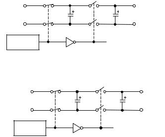
GENERAL DESCRIPTION
The ADM202E/ADM1181E are ruggedized RS-232 line drivers/ receivers. Step-up voltage converters coupled with level shifting transmitters and receivers allow RS-232 levels to be developed while operating from a single 5 V supply.
Features include low power consumption, high transmission rates and compatibility with the EU directive on Electromagnetic compatibility. EM compatibility includes protection against radiated and conducted interference including high levels of Electrostatic Discharge.
All inputs and outputs contain protection against Electrostatic Discharges up to ±15 kV and Electrical Fast Transients up to
±2 kV. This ensures compliance to IE1000-4-2 and IEC1000-4-4 requirements.
The devices are ideally suited for operation in electrically harsh environments or where RS-232 cables are frequently being plugged/unplugged. They are also immune to high RF field strengths without special shielding precautions.
CMOS technology is used to keep the power dissipation to an absolute minimum allowing maximum battery life in portable applications.
The ADM202E/ADM1181A is a modification, enhancement and improvement to the AD230–AD241 family and its derivatives. It is essentially plug-in compatible and does not have materially different applications.
CIRCUIT DESCRIPTION
The internal circuitry consists of four main sections. These are:
1.A charge pump voltage converter
2.5 V logic to EIA-232 transmitters
3.EIA-232 to 5 V logic receivers.
4.Transient protection circuit on all I/O lines
Charge Pump DC-DC Voltage Converter
The charge pump voltage converter consists of an 200 kHz oscillator and a switching matrix. The converter generates a
± 10 V supply from the input 5 V level. This is done in two stages using a switched capacitor technique as illustrated below. First, the 5 V input supply is doubled to 10 V using capacitor C1 as the charge storage element. The 10 V level is then inverted to generate –10 V using C2 as the storage element.
Capacitors C3 and C4 are used to reduce the output ripple. Their values are not critical and can be increased if desired. On the ADM202E, capacitor C3 is shown connected between V+ and VCC, while it is connected between V+ and GND on the ADM1181A. It is acceptable to use either configuration with both the ADM202E and ADM1181A. If desired, larger capacitors (up to 47 µF) can be used for capacitors C1–C4. This facilitates direct substitution with older generation charge pump RS-232 transceivers.
S1 |
S3 |
VCC |
V+ = 2VCC |
C1 |
C3 |
S2 |
S4 |
GND |
VCC |
INTERNAL
OSCILLATOR
NOTE: C3 CONNECTS BETWEEN V+ AND GND ON THE ADM1181A
Figure 1. Charge Pump Voltage Doubler
V+ |
S1 |
S3 |
|
|
GND |
||
FROM |
|
|
|
VOLTAGE |
C2 |
C4 |
|
DOUBLER |
S2 |
S4 |
|
GND |
|||
|
V– = –(V+) |
||
INTERNAL |
|
|
|
OSCILLATOR |
|
|
Figure 2. Charge Pump Voltage Inverter
Transmitter (Driver) Section
The drivers convert 5 V logic input levels into RS-232 output levels. With VCC = 5 V and driving an RS-232 load, the output voltage swing is typically ±9 V.
Receiver Section
The receivers are inverting level shifters which accept RS-232 input levels and translate them into 5 V logic output levels. The inputs have internal 5 kΩ pull-down resistors to ground and are also protected against overvoltages of up to ± 30 V.
Unconnected inputs are pulled to 0 V by the internal 5 kΩ pulldown resistor. This, therefore, results in a Logic 1 output level for unconnected inputs or for inputs connected to GND.
The receivers have Schmitt trigger inputs with a hysteresis level of 0.5 V. This ensures error-free reception for both noisy inputs and for inputs with slow transition times.
HIGH BAUD RATE
The ADM202E/ADM1181A feature high slew rates permitting data transmission at rates well in excess of the EIA/RS-232-E specifications. RS-232 voltage levels are maintained at data rates up to 230 kb/s even under worst case loading conditions. This allows for high speed data links between two terminals or indeed it is suitable for the new generation ISDN modem standards which requires data rates of 230 kbps. The slew rate is internally controlled to less than 30 V/µs in order to minimize EMI interference.
–4– |
REV. B |
Loading...