


ADF4350
Table of contents
 Loading...
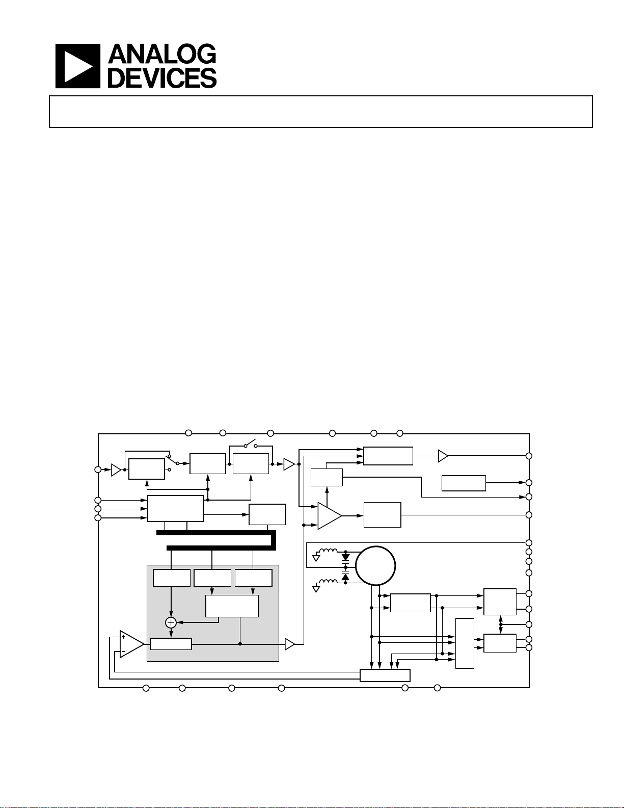
V
Wideband Synthesizer with Integrated VCO
FEATURES
Output frequency range: 137.5 MHz to 4400 MHz
Fractional-N synthesizer and integer-N synthesizer
Low phase noise VCO
Programmable divide-by-1/-2/-4/-8/-16 output
Typical rms jitter: <0.4 ps rms
Power supply: 3.0 V to 3.6 V
Logic compatibility: 1.8 V
Programmable dual-modulus prescaler of 4/5 or 8/9
Programmable output power level
RF output mute function
3-wire serial interface
Analog and digital lock detect
Switched bandwidth fast-lock mode
Cycle slip reduction
APPLICATIONS
Wireless infrastructure (W-CDMA, TD-SCDMA, WiMAX,
GSM, PCS, DCS, DECT)
Test equipment
Wireless LANs, CATV equipment
Clock generation
SDV
DD
FUNCTIONAL BLOCK DIAGRAM
AV
DD
DV
ADF4350
GENERAL DESCRIPTION
The ADF4350 allows implementation of fractional-N or
integer-N phase-locked loop (PLL) frequency synthesizers
if used with an external loop filter and external reference
frequency.
The ADF4350 has an integrated voltage controlled oscillator
(VCO) with a fundamental output frequency ranging from
2200 MHz to 4400 MHz. In addition, divide-by-1/2/4/8 or 16
circuits allow the user to generate RF output frequencies as low
as 137.5 MHz. For applications that require isolation, the RF
output stage can be muted. The mute function is both pin- and
software-controllable. An auxiliary RF output is also available,
which can be powered down if not in use.
Control of all the on-chip registers is through a simple 3-wire
interface. The device operates with a power supply ranging
from 3.0 V to 3.6 V and can be powered down when not in use.
DD
P
R
SETVVCO
REF
IN
CLK
DATA
LE
Rev. A
Information furnished by Analog Devices is believed to be accurate and reliable. However, no
responsibility is assumed by Anal og Devices for its use, nor for any infringements of patents or ot her
rights of third parties that may result from its use. Specifications subject to change without notice. No
license is granted by implication or otherwise under any patent or patent rights of Analog Devices.
Trademarks and registered trademarks are the property of their respective owners.
×2
DOUBLER
DATA REGIST ER
N COUNTER
CE
INTEGER
10-BIT R
COUNTER÷2DIVIDER
REG
FRACTION
AGND
REG
INTERPOLATOR
MODULUS
THIRD-ORDER
FRACTIONAL
DGND CP
FUNCTION
LATCH
REG
GND
MULTIPLEXER
LOCK
DETECT
PHASE
COMPARATOR
CHARGE
PUMP
VCO
CORE
÷1/2/4/8/16
MULTIPLEXER
SD
GNDAGNDVCO
FL
SWITCH
O
OUTPUT
STAGE
OUTPUT
STAGE
MULTIPLEXER
ADF4350
Figure 1.
One Technology Way, P.O. Box 9106, Norwood, MA 02062-9106, U.S.A.
Tel: 781.329.4700 www.analog.com
Fax: 781.461.3113 ©2008–2011 Analog Devices, Inc. All rights reserved.
MUXOUT
SW
LD
CP
OUT
V
TUNE
V
REF
V
COM
TEMP
RF
OUT
RF
OUT
PDB
RF
RF
OUT
RF
OUT
A+
A–
B+
B–
07325-001

ADF4350
TABLE OF CONTENTS
Features.............................................................................................. 1
Applications....................................................................................... 1
General Description ......................................................................... 1
Functional Block Diagram .............................................................. 1
Revision History ............................................................................... 2
Specifications..................................................................................... 3
Timing Characteristics ................................................................ 5
Absolute Maximum Ratings............................................................ 6
Transistor Count........................................................................... 6
ESD Caution.................................................................................. 6
Pin Configuration and Function Descriptions............................. 7
Typical Performance Characteristics ............................................. 9
Circuit Description......................................................................... 11
Reference Input Section............................................................. 11
RF N Divider............................................................................... 11
INT, FRAC, MOD, and R Counter Relationship.................... 11
INT N MODE ............................................................................. 11
R Counter ....................................................................................11
Phase Frequency Detector (PFD) and Charge Pump............ 11
MUXOUT and LOCK Detect................................................... 12
Input Shift Registers................................................................... 12
Program Modes .......................................................................... 12
VCO.............................................................................................. 12
Output Stage................................................................................ 13
Register Maps.................................................................................. 14
Register 0 .....................................................................................18
REVISION HISTORY
4/11—Rev. 0 to Rev. A
Changes to Typical rms Jitter in Features Section........................ 1
Changes to Specifications................................................................ 3
Changes Output Stage Section...................................................... 13
Changes to Figure 29...................................................................... 17
Changes to Fast Lock—An Example Section.............................. 22
Changes to Direct Conversion Modulator Section and
Figure 34 .........................................................................................25
Changes to ADuC70xx Interface Section and ADSP-BF527
Interface Section ............................................................................. 26
Changes to Output Matching Section and Table 7..................... 27
Added Table 8.................................................................................. 28
Changes to Ordering Guide.......................................................... 29
11/08—Revision 0: Initial Version
Rev. A | Page 2 of 32
Register 1 ..................................................................................... 18
Register 2 ..................................................................................... 18
Register 3 ..................................................................................... 20
Register 4 ..................................................................................... 20
Register 5 ..................................................................................... 20
Initialization Sequence .............................................................. 21
RF Synthesizer—A Worked Example ...................................... 21
Modulus....................................................................................... 21
Reference Doubler and Reference Divider ............................. 21
12-Bit Programmable Modulus................................................ 21
Cycle Slip Reduction for Faster Lock Times........................... 22
Spurious Optimization and Fast lock ...................................... 22
Fast-Lock Timer and Register Sequences ............................... 22
Fast Lock—An Example............................................................ 22
Fast Lock—Loop Filter Topology............................................. 23
Spur Mechanisms....................................................................... 23
Spur Consistency and Fractional Spur Optimization ........... 24
Phase Resync............................................................................... 24
Applications Information.............................................................. 25
Direct Conversion Modulator .................................................. 25
Interfacing ................................................................................... 26
PCB Design Guidelines for a Chip Scale Package ................. 26
Output Matching........................................................................ 27
Outline Dimensions....................................................................... 29
Ordering Guide .......................................................................... 29

ADF4350
SPECIFICATIONS
AVDD = DVDD = V
temperature range is −40°C to +85°C.
Table 1.
Parameter
REFIN CHARACTERISTICS
Input Frequency 10 250 MHz For f < 10 MHz ensure slew rate > 21 V/μs
Input Sensitivity 0.7 AVDD V p-p Biased at AVDD/21
Input Capacitance 10 pF
Input Current ±60 μA
PHASE DETECTOR
Phase Detector Frequency2 32 MHz
CHARGE PUMP
ICP Sink/Source3 With R
High Value 5 mA
Low Value 0.312 mA
R
Range 2.7 10 kΩ
SET
Sink and Source Current Matching 2 % 0.5 V ≤ VCP ≤ 2.5 V
ICP vs. VCP 1.5 % 0.5 V ≤ VCP ≤ 2.5 V
ICP vs. Temperature 2 % VCP = 2.0 V
LOGIC INPUTS
Input High Voltage, V
Input Low Voltage, V
Input Current, I
Input Capacitance, CIN 3.0 pF
LOGIC OUTPUTS
Output High Voltage, VOH DVDD − 0.4 V CMOS output chosen
Output High Current, IOH 500 μA
Output Low Voltage, VOL 0.4 V IOL = 500 μA
POWER SUPPLIES
AVDD 3.0 3.6 V
DVDD, V
DIDD + AI
Output Dividers 6 to 24 mA Each output divide-by-2 consumes 6 mA
I
VCO
I
RFOUT
Low Power Sleep Mode 7 1000 μA
RF OUTPUT CHARACTERISTICS
Maximum VCO Output Frequency 4400 MHz
Minimum VCO Output Frequency 2200 MHz Fundamental VCO mode
Minimum VCO Output Frequency
VCO Sensitivity 33 MHz/V
Frequency Pushing (Open-Loop) 1 MHz/V
Frequency Pulling (Open-Loop) 90 kHz Into 2.00 VSWR load
Harmonic Content (Second) −19 dBc Fundamental VCO output
Harmonic Content (Third) −13 dBc Fundamental VCO output
Harmonic Content (Second) −20 dBc Divided VCO output
Harmonic Content (Third) −10 dBc Divided VCO output
Minimum RF Output Power 5 −4 dBm Programmable in 3 dB steps
Maximum RF Output Power5 5 dBm
Output Power Variation ±1 dB
Minimum VCO Tuning Voltage 0.5 V
Maximum VCO Tuning Voltage 2.5 V
, SD
VCO
4
21 27 mA
DD
4
4
Using Dividers
= SDVDD = VP = 3.3 V ± 10%; AGND = DGND = 0 V; TA = T
VCO
MIN
to T
, unless otherwise noted. Operating
MAX
B Version
Min Typ Max
1.5 V
INH
0.6 V
INL
±1 μA
INH/IINL
, VP AVDD These voltages must equal AVDD
VDD
Unit Conditions/Comments
= 5.1 kΩ
SET
70 80 mA
21 26 mA RF output stage is programmable
137.5 MHz 2200 MHz fundamental output and divide by 16 selected
Rev. A | Page 3 of 32

ADF4350
B Version
Parameter
Min Typ Max
NOISE CHARACTERISTICS
VCO Phase-Noise Performance6 −89 dBc/Hz 10 kHz offset from 2.2 GHz carrier
−114 dBc/Hz 100 kHz offset from 2.2 GHz carrier
−134 dBc/Hz 1 MHz offset from 2.2 GHz carrier
−148 dBc/Hz 5 MHz offset from 2.2 GHz carrier
−86 dBc/Hz 10 kHz offset from 3.3 GHz carrier
−111 dBc/Hz 100 kHz offset from 3.3 GHz carrier
−134 dBc/Hz 1 MHz offset from 3.3 GHz carrier
−145 dBc/Hz 5 MHz offset from 3.3 GHz carrier
−83 dBc/Hz 10 kHz offset from 4.4 GHz carrier
−110 dBc/Hz 100 kHz offset from 4.4 GHz carrier
−132 dBc/Hz 1 MHz offset from 4.4 GHz carrier
−145 dBc/Hz 5 MHz offset from 4.4 GHz carrier
Normalized Phase Noise Floor
)7
(PN
SYNTH
Normalized 1/f Noise (PN
)8 −111 dBc/Hz 10 kHz offset; normalized to 1 GHz
1_f
−220 dBc/Hz PLL Loop BW = 500 kHz
In-Band Phase Noise9 −97 dBc/Hz 3 kHz offset from 2113.5 MHz carrier
Integrated RMS Jitter10 0.5 ps
Spurious Signals Due to PFD Frequency −70 dBc
Level of Signal With RF Mute Enabled −40 dBm
1
AC coupling ensures AVDD/2 bias.
2
Guaranteed by design. Sample tested to ensure compliance.
3
ICP is internally modified to maintain constant loop gain over the frequency range.
4
TA = 25°C; AVDD = DVDD = V
5
Using 50 Ω resistors to V
main output.
6
The noise of the VCO is measured in open-loop conditions.
7
The synthesizer phase noise floor is estimated by measuring the in-band phase noise at the output of the VCO and subtracting 20 log N (where N is the N divider
value) and 10 log F
8
The PLL phase noise is composed of 1/f (flicker) noise plus the normalized PLL noise floor. The formula for calculating the 1/f noise contribution at an RF frequency, fRF,
and at a frequency offset f is given by PN = P
9
f
= 100 MHz; f
REFIN
ICP = 313 μA; low noise mode. The noise was measured with an EVAL-ADF4350EB1Z and the Agilent E5052A signal source analyzer.
10
f
= 100 MHz; f
REFIN
an EVAL-ADF4350EB1Z and the Agilent E5052A signal source analyzer.
PFD
PFD
PFD
= 3.3 V; prescaler = 8/9; f
VCO
, into a 50 Ω load. Power measured with auxiliary RF output disabled. The current consumption of the auxiliary output is the same as for the
VCO
. PN
= PN
SYNTH
= 25 MHz; offset frequency = 10 kHz; VCO frequency = 4227 MHz, output divide by two enabled. RF
− 10 log F
TOT
+ 10log(10 kHz/f) + 20log(fRF/1 GHz). Both the normalized phase noise floor and flicker noise are modeled in ADIsimPLL.
1_f
= 25 MHz; VCO frequency = 4400 MHz, RF
REFIN
− 20 log N.
PFD
= 100 MHz; f
OUT
= 25 MHz; fRF = 4.4 GHz.
PFD
= 4400 MHz; N = 176; loop BW = 40 kHz, ICP = 313 μA; low noise mode. The noise was measured with
Unit Conditions/Comments
= 2113.5 MHz; N = 169; loop BW = 40 kHz,
OUT
Rev. A | Page 4 of 32
ADF4350
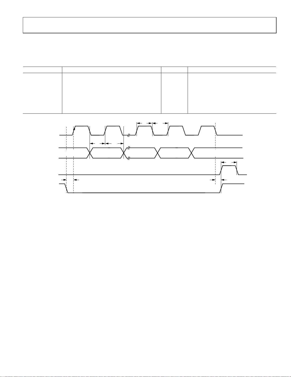
TIMING CHARACTERISTICS
AVDD = DVDD = V
otherwise noted.
Table 2.
Parameter Limit (B Version) Unit Test Conditions/Comments
t1 20 ns min LE setup time
t2 10 ns min DATA to CLK setup time
t3 10 ns min DATA to CLK hold time
t4 25 ns min CLK high duration
t5 25 ns min CLK low duration
t6 10 ns min CLK to LE setup time
t7 20 ns min LE pulse width
= SDVDD = VP = 3.3 V ± 10%; AGND = DGND = 0 V; 1.8 V and 3 V logic levels used; TA = T
VCO
CLK
t
4
t
5
MIN
to T
MAX
, unless
DATA
t
2
DB31 (MSB) DB30
LE
t
1
LE
t
3
DB2
(CONTROL BIT C3)
DB1
(CONTROL BIT C2)
DB0 (LSB)
(CONTROL BIT C1)
t
6
t
7
07325-002
Figure 2. Timing Diagram
Rev. A | Page 5 of 32
ADF4350
ABSOLUTE MAXIMUM RATINGS
TA = 25°C, unless otherwise noted.
Table 3.
Parameter Rating
AVDD to GND1 −0.3 V to +3.9 V
AVDD to DVDD −0.3 V to +0.3 V
V
to GND −0.3 V to +3.9 V
VCO
V
to AVDD −0.3 V to +0.3 V
VCO
Digital I/O Voltage to GND −0.3 V to VDD + 0.3 V
Analog I/O Voltage to GND −0.3 V to VDD + 0.3 V
REFIN to GND −0.3 V to VDD + 0.3 V
Operating Temperature Range −40°C to +85°C
Storage Temperature Range −65°C to +125°C
Maximum Junction Temperature 150°C
LFCSP θJA Thermal Impedance 27.3°C/W
(Paddle-Soldered)
Reflow Soldering
Peak Temperature 260°C
Time at Peak Temperature 40 sec
1
GND = AGND = DGND = 0 V
Stresses above those listed under Absolute Maximum Ratings
may cause permanent damage to the device. This is a stress
rating only; functional operation of the device at these or any
other conditions above those indicated in the operational
section of this specification is not implied. Exposure to absolute
maximum rating conditions for extended periods may affect
device reliability.
This device is a high-performance RF integrated circuit with an
ESD rating of <0.5 kV and is ESD sensitive. Proper precautions
should be taken for handling and assembly.
TRANSISTOR COUNT
24202 (CMOS) and 918 (bipolar)
ESD CAUTION
Rev. A | Page 6 of 32
ADF4350
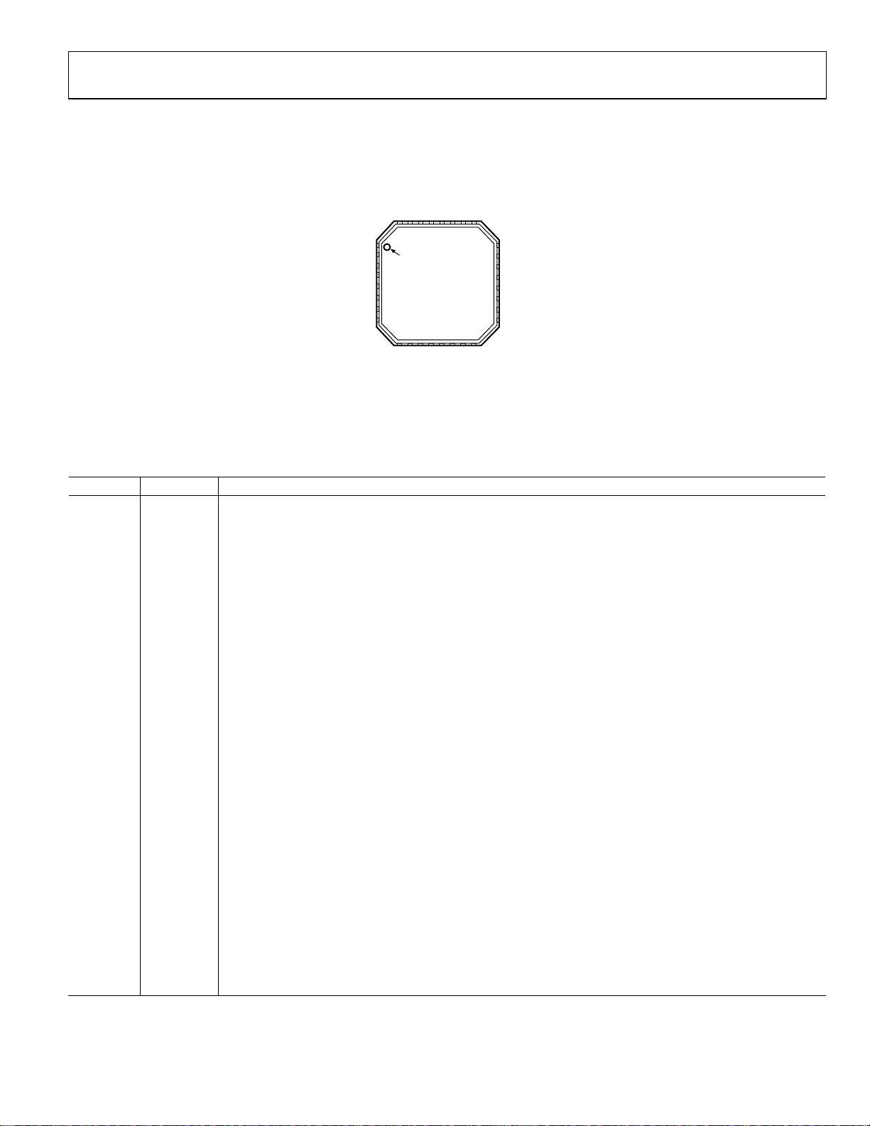
PIN CONFIGURATION AND FUNCTION DESCRIPTIONS
DD
IN
DD
GND
SDV
REF
DGND13DV
SD
MUXOUT
PDBRFLD
TOP VIEW
11
12
DD
A+
OUT
GNDVCO
A
RF
27
26
25
24
V
REF
23
V
COM
22
R
SET
21
A
GNDVCO
20
V
TUNE
19
TEM
P
18
A
GNDVCO
17
V
VCO
141516
B+
A−
B−
VCO
V
OUT
OUT
OUT
RF
RF
RF
to the external loop filter. The output of the loop filter is
CP
must have the same value as DVDD.
DD
must have the same value as AVDD.
VCO
07325-003
. Decoupling capacitors to the ground plane are to
DD
.
OUT
OUT
3231302928
1
CLK
DATA
LE
CE
SW
V
P
CP
OUT
CP
GND
NOTES
1. THE LFCSP HAS AN EXPOS ED PADDLE THAT MUST BE CONNECT ED TO GND.
2
3
4
5
6
7
8
PIN 1
INDICAT OR
ADF4350
(Not to Scale)
9
10
AGND
AV
Figure 3. Pin Configuration
Table 4. Pin Function Descriptions
Pin No. Mnemonic Description
1 CLK
Serial Clock Input. Data is clocked into the 32-bit shift register on the CLK rising edge. This input is a high
impedance CMOS input.
2 DATA
Serial Data Input. The serial data is loaded MSB first with the three LSBs as the control bits. This input is a high
impedance CMOS input.
3 LE
Load Enable, CMOS Input. When LE goes high, the data stored in the shift register is loaded into the register
that is selected by the three LSBs.
4 CE
Chip Enable. A logic low on this pin powers down the device and puts the charge pump into three-state mode.
A logic high on this pin powers up the device depending on the status of the power-down bits.
5 SW Fast-Lock Switch. A connection should be made from the loop filter to this pin when using the fast-lock mode.
6 VP
Charge Pump Power Supply. This pin is to be equal to AV
be placed as close as possible to this pin.
7 CP
8 CP
OUT
Charge Pump Ground. This is the ground return pin for CP
GND
Charge Pump Output. When enabled, this provides ±I
connected to V
to drive the internal VCO.
TUNE
9 AGND Analog Ground. This is a ground return pin for AVDD.
10 AVDD
Analog Power Supply. This pin ranges from 3.0 V to 3.6 V. Decoupling capacitors to the analog ground plane are
to be placed as close as possible to this pin. AV
11, 18, 21 A
12 RF
13 RF
VCO Analog Ground. These are the ground return pins for the VCO.
GNDVCO
A+ VCO Output. The output level is programmable. The VCO fundamental output or a divided down version is available.
OUT
OUT
A−
Complementary VCO Output. The output level is programmable. The VCO fundamental output or a divided
down version is available.
14 RF
OUT
B+
Auxilliary VCO Output. The output level is programmable. The VCO fundamental output or a divided down
version is available.
15 RF
OUT
B−
Complementary Auxilliary VCO Output. The output level is programmable. The VCO fundamental output or a
divided down version is available.
16, 17 V
VCO
Power Supply for the VCO. This ranges from 3.0 V to 3.6 V. Decoupling capacitors to the analog ground plane
should be placed as close as possible to these pins. V
19 TEMP
Temperature Compensation Output. Decoupling capacitors to the ground plane are to be placed as close as
possible to this pin.
20 V
TUNE
Control Input to the VCO. This voltage determines the output frequency and is derived from filtering the CP
output voltage.
Rev. A | Page 7 of 32

ADF4350
Pin No. Mnemonic Description
22 R
23 V
24 V
25 LD Lock Detect Output Pin. This pin outputs a logic high to indicate PLL lock. A logic low output indicates loss of PLL lock.
26 PDBRF RF Power-Down. A logic low on this pin mutes the RF outputs. This function is also software controllable.
27 DGND Digital Ground. Ground return path for DVDD.
28 DVDD
29 REFIN
30 MUXOUT
31 SD
32 SDVDD
33 EP Exposed Pad.
SET
Connecting a resistor between this pin and GND sets the charge pump output current. The nominal voltage
bias at the R
I =
CP
pin is 0.55 V. The relationship between ICP and R
SET
25.5
R
SET
SET
is
where:
= 5.1 kΩ
R
SET
I
= 5 mA
CP
COM
Internal Compensation Node Biased at Half the Tuning Range. Decoupling capacitors to the ground plane
should be placed as close as possible to this pin.
Reference Voltage. Decoupling capacitors to the ground plane should be placed as close as possible to this pin.
REF
Digital Power Supply. This pin should be the same voltage as AV
. Decoupling capacitors to the ground plane
DD
should be placed as close as possible to this pin.
Reference Input. This is a CMOS input with a nominal threshold of V
/2 and a dc equivalent input resistance of
DD
100 kΩ. This input can be driven from a TTL or CMOS crystal oscillator, or it can be ac-coupled.
Multiplexer Output. This multiplexer output allows either the lock detect, the scaled RF, or the scaled reference
frequency to be accessed externally.
Digital Sigma-Delta (Σ-Δ) Modulator Ground. Ground return path for the Σ-Δ modulator.
GND
Power Supply Pin for the Digital Σ-Δ Modulator. Should be the same voltage as AV
. Decoupling capacitors to
DD
the ground plane are to be placed as close as possible to this pin.
Rev. A | Page 8 of 32

ADF4350
–
–
–
–
–
–
TYPICAL PERFORMANCE CHARACTERISTICS
40
–50
–60
–70
–80
–90
–100
–110
–120
PHASE NOISE (dBc/Hz)
–130
–140
–150
–160
1k 10k 100k 1M 10M 100M
FREQUENCY (Hz)
Figure 4. Open-Loop VCO Phase Noise, 2.2 GHz
07325-028
70
–80
–90
–100
–110
–120
–130
–140
PHASE NOISE (dBc/Hz)
–150
–160
–170
1k 10k 100k 1M 10M 100M
FREQUENCY (Hz)
FUND
DIV2
DIV4
DIV8
DIV16
Figure 7. Closed-Loop Phase Noise, Fundamental VCO and Dividers,
VCO = 2.2 GHz, PFD = 25 MHz, Loop Bandwidth = 40 kHz
07325-031
40
–50
–60
–70
–80
–90
–100
–110
–120
PHASE NOISE (dBc/Hz)
–130
–140
–150
–160
1k 10k 100k 1M 10M 10 0M
FREQUENCY (Hz)
Figure 5. Open-Loop VCO Phase Noise, 3.3 GHz
40
–50
–60
–70
–80
–90
–100
–110
–120
PHASE NOISE (d Bc/Hz)
–130
–140
–150
–160
1k 10k 100k 1M 10M 100M
FREQUENCY (Hz)
Figure 6. Open-Loop VCO Phase Noise, 4.4 GHz
70
–80
–90
–100
–110
–120
–130
–140
PHASE NOISE (dBc/Hz)
PHASE NOISE (dBc/Hz)
–150
–160
–170
1k 10k 100k 1M 10M 100M
07325-029
FREQUENCY (Hz)
FUND
DIV2
DIV4
DIV8
DIV16
07325-032
Figure 8. Closed-Loop Phase Noise, Fundamental VCO and Dividers,
VCO = 3.3 GHz, PFD = 25 MHz, Loop Bandwidth = 40 kHz
70
–80
–90
–100
–110
–120
–130
–140
PHASE NOISE (dBc/Hz)
–150
–160
–170
1k 10k 100k 1M 10M 100M
07325-030
FREQUENCY (Hz)
FUND
DIV2
DIV4
DIV8
DIV16
07325-033
Figure 9. Closed-Loop Phase Noise, Fundamental VCO and Dividers,
VCO = 4.4 GHz, PFD = 25 MHz, Loop Bandwidth = 40 kHz
Rev. A | Page 9 of 32

ADF4350
0
0
–20
–40
–60
–80
–100
PHASE NOISE ( dBc/Hz)
–120
–140
–160
1k 10k
100k 1M
FREQUENCY ( Hz)
10M
Figure 10. Integer-N Phase Noise and Spur Performance. GSM900 Band,
= 904 MHz, REFIN = 100 MHz, PFD = 800 kHz, Output Divide-by-4
RF
OUT
Selected; Loop-Filter Bandwidth = 16 kHz, Channel Spacing = 200 kHz.
0
–20
–40
–60
–80
–100
PHASE NOISE ( dBc/Hz)
–120
–20
–40
–60
–80
–100
PHASE NOISE ( dBc/Hz)
–120
–140
–160
07325-034
1k 10k
Figure 13. Fractional-N Spur Performance. Low Noise Mode, RF
2.591 GHz, REF
= 105 MHz, PFD = 17.5 MHz, Output Divide-by-1 Selected;
IN
100k 1M
FREQUENCY ( Hz)
10M
OUT
07325-037
=
Loop Filter Bandwidth = 20 kHz, Channel Spacing = 100 kHz.
0
–20
–40
–60
–80
–100
PHASE NOISE ( dBc/Hz)
–120
–140
–160
1k 10k
100k 1M
FREQUENCY ( Hz)
10M
07325-035
Figure 11. Fractional-N Spur Performance; Low Noise Mode. W-CDMA Band,
= 2113.5 MHz, REFIN = 100 MHz, PFD = 25 MHz, Output Divide-by-2
RF
OUT
Selected; Loop Filter Bandwidth = 40 kHz, Channel Spacing = 200 kHz.
0
–20
–40
–60
–80
–100
PHASE NOISE ( dBc/Hz)
–120
–140
–160
1k 10k
100k 1M
FREQUENCY ( Hz)
10M
07325-036
Figure 12. Fractional-N Spur Performance. Low Spur Mode, W-CDMA Band
= 2113.5 MHz, REFIN = 100 MHz, PFD = 25 MHz, Output Divide-by-2
RF
OUT
Selected; Loop Filter Bandwidth = 40 kHz, Channel Spacing = 200 kHz
–140
–160
1k 10k
Figure 14. Fractional-N Spur Performance. Low Spur Mode RF
2.591 GHz, REF
= 105 MHz, PFD = 17.5 MHz, Output Divide-by-1 Selected.
IN
100k 1M
FREQUENCY ( Hz)
10M
OUT
07325-038
=
Loop Filter Bandwidth = 20 kHz, Channel Spacing = 100 kHz (Note That
Fractional Spurs Are Removed and Only the Integer Boundary Spur Remains
in Low Spur Mode).
3.02
3.01
3.00
2.99
2.98
FREQUENC Y (GHz)
2.97
2.96
2.95
0 100 200 300
CSR OFF
CSR ON
TIME (µs)
400 500 600
07325-039
Figure 15. Lock Time for 100 MHz Jump from 3070 MHz to 2970 MHz with
CSR On and Of f, PFD = 25 MHz, I
= 313 μA, Loop Filter Bandwidth = 20 kHz
CP
Rev. A | Page 10 of 32
Loading...