


Analog Devices AD815-EB, AD815AYS, AD815AY, AD815AVR, AD815AV Datasheet
...a |
High Output Current |
|
Differential Driver |
||
|
|
|
|
|
AD815 |
|
|
|
FEATURES
Flexible Configuration
Differential Input and Output Driver or Two Single-Ended Drivers
High Output Power
Power Package
26 dBm Differential Line Drive for ADSL Application 40 V p-p Differential Output Voltage, RL = 50 V 500 mA Minimum Output Drive/Amp, RL = 5 V
Thermally Enhanced SOIC
400 mA Minimum Output Drive/Amp, RL = 10 V
Low Distortion
–66 dB @ 1 MHz THD, RL = 200 V, VOUT = 40 V p-p 0.05% and 0.458 Differential Gain and Phase, RL = 25 V
(6 Back-Terminated Video Loads) High Speed
120 MHz Bandwidth (–3 dB)
900 V/ms Differential Slew Rate
70 ns Settling Time to 0.1% Thermal Shutdown
APPLICATIONS
ADSL, HDSL and VDSL Line Interface Driver Coil or Transformer Driver
CRT Convergence and Astigmatism Adjustment Video Distribution Amp
Twisted Pair Cable Driver
PRODUCT DESCRIPTION
The AD815 consists of two high speed amplifiers capable of supplying a minimum of 500 mA. They are typically configured as a differential driver enabling an output signal of 40 V p-p on
± 15 V supplies. This can be increased further with the use of a
|
–40 |
|
|
|
|
|
dBc |
|
VS = 615V |
|
|
|
|
–50 |
G = +10 |
|
|
|
|
|
VOUT = 40V p-p |
|
|
|
|
||
– |
|
|
|
|
|
|
DISTORTION |
–60 |
|
|
|
|
|
–70 |
|
|
|
|
|
|
|
|
|
|
|
|
|
HARMONIC |
–80 |
RL = 50V |
|
|
|
|
(DIFFERENTIAL) |
|
|
|
|||
|
|
|
|
|||
–90 |
|
|
RL = 200V |
|
||
|
|
(DIFFERENTIAL) |
|
|||
|
|
|
|
|||
TOTAL |
|
|
|
|
||
–100 |
|
|
|
|
|
|
|
|
|
|
|
|
|
|
–110 |
|
10k |
100k |
1M |
|
|
100 |
1k |
10M |
|||
|
|
|
FREQUENCY – Hz |
|
|
|
Total Harmonic Distortion vs. Frequency
REV. B
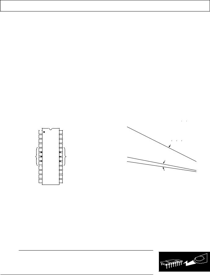
FUNCTIONAL BLOCK DIAGRAM
15-Lead Through-Hole SIP (Y) and Surface-Mount
|
DDPAK(VR) |
|
|
|
|
15 |
NC |
|
|
14 |
NC |
TAB IS |
|
13 |
NC |
|
12 |
NC |
|
+VS |
|
||
|
11 |
+IN2 |
|
|
|
||
|
|
10 |
–IN2 |
|
|
9 |
OUT2 |
|
AD815 |
8 |
+VS |
|
7 |
–VS |
|
|
|
||
|
|
6 |
OUT1 |
|
|
5 |
–IN1 |
|
|
4 |
+IN1 |
3 |
|
|
|
|
NC |
2 |
|
|
|
|
NC |
|
|
|
|
||
1 |
|
|
|
|
NC |
|
|
|
|
NC = NO CONNECT
REFER TO PAGE 3 FOR 24-LEAD SOIC PACKAGE
coupling transformer with a greater than 1:1 turns ratio. The low harmonic distortion of –66 dB @ 1 MHz into 200 Ω combined with the wide bandwidth and high current drive make the differential driver ideal for communication applications such as subscriber line interfaces for ADSL, HDSL and VDSL.
The AD815 differential slew rate of 900 V/µs and high load drive are suitable for fast dynamic control of coils or transformers, and the video performance of 0.05% and 0.45° differential gain and phase into a load of 25 Ω enable up to 12 back-terminated loads to be driven.
Three package styles are available, and all work over the industrial temperature range (–40°C to +85°C). Maximum output power is achieved with the power package available for through-hole mounting (Y) and surface-mounting (VR). The 24-lead SOIC (RB) is capable of driving 26 dBm for full rate ADSL with proper heat sinking.
|
|
|
|
+15V |
|
|
|
|
|
|
100V |
1/2 |
|
|
|
|
|
|
|
AD815 |
R1 |
= 15V |
|
|
|
|
|
AMP1 |
|
||
|
|
|
|
|
|
|
|
|
|
|
|
499V |
|
|
|
V |
IN |
= |
|
|
V = |
RL |
V = |
|
|
110V |
G = +10 |
D |
|
||
4Vp-p |
40Vp-p |
120V |
OUT |
||||
|
|
40Vp-p |
|||||
|
|
|
|
|
|
|
|
|
|
|
|
AMP2 |
R2 = 15V |
|
|
|
|
|
100V |
|
1:2 |
|
|
|
|
|
|
|
|
||
|
|
|
|
|
|
|
|
|
|
|
|
|
|
TRANSFORMER |
|
|
|
|
|
–15V |
|
|
|
Subscriber Line Differential Driver
Information furnished by Analog Devices is believed to be accurate and reliable. However, no responsibility is assumed by Analog Devices for its use, nor for any infringements of patents or other rights of third parties which may result from its use. No license is granted by implication or otherwise under any patent or patent rights of Analog Devices.
One Technology Way, P.O. Box 9106, Norwood, MA 02062-9106, U.S.A.
Tel: 781/329-4700 |
World Wide Web Site: http://www.analog.com |
Fax: 781/326-8703 |
© Analog Devices, Inc., 1999 |
AD815–SPECIFICATIONS (@ TA = +258C, VS = 615 V dc, RFB = 1 kV and RLOAD = 100 V unless otherwise noted)
|
|
|
|
AD815A |
|
|
Model |
Conditions |
VS |
Min |
Typ |
Max |
Units |
DYNAMIC PERFORMANCE |
|
±15 |
|
|
|
|
Small Signal Bandwidth (–3 dB) |
G = +1 |
100 |
120 |
|
MHz |
|
|
G = +1 |
±5 |
90 |
110 |
|
MHz |
Bandwidth (0.1 dB) |
G = +2 |
±15 |
|
40 |
|
MHz |
|
G = +2 |
±5 |
|
10 |
|
MHz |
Differential Slew Rate |
VOUT = 20 V p-p, G = +2 |
±15 |
800 |
900 |
|
V/µs |
Settling Time to 0.1% |
10 V Step, G = +2 |
±15 |
|
70 |
|
ns |
NOISE/HARMONIC PERFORMANCE |
f = 1 MHz, RLOAD = 200 Ω, VOUT = 40 V p-p |
±15 |
|
–66 |
|
dBc |
Total Harmonic Distortion |
|
|
||||
Input Voltage Noise |
f = 10 kHz, G = +2 (Single Ended) |
±5, ±15 |
|
1.85 |
|
nV/√Hz |
Input Current Noise (+IIN) |
f = 10 kHz, G = +2 |
±5, ±15 |
|
1.8 |
|
pA/√Hz |
Input Current Noise (–IIN) |
f = 10 kHz, G = +2 |
±5, ±15 |
|
19 |
|
pA/√Hz |
Differential Gain Error |
NTSC, G = +2, RLOAD = 25 Ω |
±15 |
|
0.05 |
|
% |
Differential Phase Error |
NTSC, G = +2, RLOAD = 25 Ω |
±15 |
|
0.45 |
|
Degrees |
DC PERFORMANCE |
|
±5 |
|
|
|
|
Input Offset Voltage |
|
|
5 |
8 |
mV |
|
|
TMIN – TMAX |
±15 |
|
10 |
15 |
mV |
|
|
|
|
30 |
mV |
|
Input Offset Voltage Drift |
|
±5 |
|
20 |
|
µV/°C |
Differential Offset Voltage |
|
|
0.5 |
2 |
mV |
|
|
|
±15 |
|
0.5 |
4 |
mV |
|
TMIN – TMAX |
|
|
|
5 |
mV |
Differential Offset Voltage Drift |
|
|
|
10 |
|
µV/°C |
–Input Bias Current |
|
±5, ±15 |
|
10 |
90 |
µA |
|
TMIN – TMAX |
±5, ±15 |
|
|
150 |
µA |
+Input Bias Current |
|
|
2 |
5 |
µA |
|
|
TMIN – TMAX |
±5, ±15 |
|
|
5 |
µA |
Differential Input Bias Current |
|
|
10 |
75 |
µA |
|
|
TMIN – TMAX |
±5, ±15 |
|
|
100 |
µA |
Open-Loop Transresistance |
|
1.0 |
5.0 |
|
MΩ |
|
|
TMIN – TMAX |
|
0.5 |
|
|
MΩ |
INPUT CHARACTERISTICS |
|
±15 |
|
|
|
MΩ |
Differential Input Resistance |
+Input |
|
7 |
|
||
|
–Input |
±15 |
|
15 |
|
Ω |
Differential Input Capacitance |
|
|
1.4 |
|
pF |
|
Input Common-Mode Voltage Range |
|
±15 |
|
13.5 |
|
±V |
|
|
±5 |
|
3.5 |
|
±V |
Common-Mode Rejection Ratio |
TMIN – TMAX |
±5, ±15 |
57 |
65 |
|
dB |
Differential Common-Mode Rejection Ratio |
TMIN – TMAX |
±5, ±15 |
80 |
100 |
|
dB |
OUTPUT CHARACTERISTICS |
Single Ended, RLOAD = 25 Ω |
±15 |
|
|
|
±V |
Voltage Swing |
11.0 |
11.7 |
|
|||
|
|
±5 |
1.1 |
1.8 |
|
±V |
|
Differential, RLOAD = 50 Ω |
±15 |
21 |
23 |
|
±V |
Output Current1, 2 |
TMIN – TMAX |
±15 |
22.5 |
24.5 |
|
±V |
RLOAD = 5 Ω |
±15 |
|
|
|
|
|
VR, Y |
500 |
750 |
|
mA |
||
|
|
±5 |
350 |
400 |
|
mA |
RB-24 |
RLOAD = 10 Ω |
±15 |
400 |
500 |
|
mA |
Short Circuit Current |
|
±15 |
|
1.0 |
|
A |
Output Resistance |
|
±15 |
|
13 |
|
Ω |
MATCHING CHARACTERISTICS |
|
±15 |
|
|
|
|
Crosstalk |
f = 1 MHz |
|
–65 |
|
dB |
|
POWER SUPPLY |
|
|
|
|
±18 |
|
Operating Range3 |
TMIN – TMAX |
±5 |
|
|
V |
|
Quiescent Current |
|
|
23 |
30 |
mA |
|
|
|
±15 |
|
30 |
40 |
mA |
|
TMIN – TMAX |
±5 |
|
|
40 |
mA |
|
|
±15 |
|
|
55 |
mA |
Power Supply Rejection Ratio |
TMIN – TMAX |
±5, ±15 |
–55 |
–66 |
|
dB |
NOTES
1Output current is limited in the 24-lead SOIC package to the maximum power dissipation. See absolute maximum ratings and derating curves. 2See Figure 12 for bandwidth, gain, output drive recommended operation range.
3Observe derating curves for maximum junction temperature. Specifications subject to change without notice.
–2– |
REV. B |
AD815
ABSOLUTE MAXIMUM RATINGS1 |
±18 V Total |
|
Supply Voltage . . . . . . . . |
. . . . . . . . . . . . . . . . |
|
Internal Power Dissipation2 |
|
|
Plastic (Y and VR) . . |
3.05 Watts (Observe Derating Curves) |
|
Small Outline (RB) . . |
2.4 Watts (Observe Derating Curves) |
|
Input Voltage (Common Mode) . . . . . . . . . . |
. . . . . . . . . . ±VS |
|
Differential Input Voltage . . . . . . . . . . . . . . . |
. . . . . . . . . ±6 V |
|
Output Short Circuit Duration |
|
|
. . . . . . . . . . . . . . . . . . |
. . . . Observe Power Derating Curves |
|
|
Can Only Short to Ground |
|
Storage Temperature Range |
–65°C to +125°C |
|
Y, VR and RB Package |
. . . . . . . . . . . . . . . |
|
Operating Temperature Range |
–40°C to +85°C |
|
AD815A . . . . . . . . . . . |
. . . . . . . . . . . . . . . . |
|
Lead Temperature Range (Soldering, 10 sec) |
. . . . . . . +300°C |
|
NOTES
1Stresses above those listed under Absolute Maximum Ratings may cause permanent damage to the device. This is a stress rating only; functional operation of the device at these or any other conditions above those indicated in the operational section of this specification is not implied. Exposure to absolute maximum rating conditions for extended periods may affect device reliability.
2Specification is for device in free air with 0 ft/min air flow: 15-Lead Through-Hole and Surface Mount: θJA = 41°C/W; 24-Lead Surface Mount: θJA = 52°C/W.
PIN CONFIGURATION
24-Lead Thermally-Enhanced SOIC (RB-24)
NC |
1 |
24 |
NC |
NC |
2 |
23 |
NC |
NC |
3 |
22 |
NC |
NC |
4 |
21 NC |
|
|
5 |
AD815 |
20 |
|
|
THERMAL |
6 |
19 |
THERMAL |
||
TOP VIEW |
|||||
HEAT TABS |
|
|
HEAT TABS |
||
7 |
(Not to Scale) |
18 |
|||
+VS* |
+VS* |
||||
|
|
|
|||
|
8 |
|
17 |
|
|
+IN1 |
9 |
|
16 |
+IN2 |
|
–IN1 |
10 |
|
15 |
–IN2 |
|
OUT1 |
11 |
|
14 |
OUT2 |
|
–VS |
12 |
|
13 |
+VS |
NC = NO CONNECT
*HEAT TABS ARE CONNECTED TO THE POSITIVE SUPPLY.
MAXIMUM POWER DISSIPATION
The maximum power that can be safely dissipated by the AD815 is limited by the associated rise in junction temperature. The maximum safe junction temperature for the plastic encapsulated parts is determined by the glass transition temperature of the plastic, about 150°C. Exceeding this limit temporarily may cause a shift in parametric performance due to a change in the stresses exerted on the die by the package. Exceeding a junction temperature of 175°C for an extended period can result in device failure.
The AD815 has thermal shutdown protection, which guarantees that the maximum junction temperature of the die remains below a safe level, even when the output is shorted to ground. Shorting the output to either power supply will result in device failure. To ensure proper operation, it is important to observe the derating curves and refer to the section on power considerations.
It must also be noted that in high (noninverting) gain configurations (with low values of gain resistor), a high level of input overdrive can result in a large input error current, which may result in a significant power dissipation in the input stage. This power must be included when computing the junction temperature rise due to total internal power.
|
14 |
|
|
|
|
|
|
|
|
|
|
|
|
|
|
|
|
|
|
|
|
|
|
|
|
|
|
|
|
|
|
|
|
|
|
|
|
|
|
|
|
TJ = 1508C |
|
|
|
||||||
|
13 |
|
|
|
|
|
|
|
|
|
|
|
|
|
|
|
|
|
|
||||||
Watts |
12 |
|
|
|
|
|
|
|
|
|
|
|
|
|
|
|
|
|
|
|
|
|
|
|
|
|
|
|
|
|
|
|
|
|
|
θJA = 168C/W |
|
|
|
|
|
|
|
|
|
||||||
|
|
|
|
|
|
|
|
|
|
|
|
|
|
|
|
|
|
|
|||||||
– |
11 |
|
|
|
|
|
|
|
|
|
|
SOLDERED DOWN TO |
|
|
|
|
|
||||||||
|
|
|
|
|
|
|
|
|
|
|
|
|
|
|
|||||||||||
DISSIPATION |
7 |
|
|
|
|
|
|
|
|
|
|
COPPER HEAT SINK |
|
|
|
|
|
||||||||
|
10 |
|
|
|
|
|
|
|
|
|
|
(STILL AIR = 0FT/MIN) |
|
|
|
|
|
||||||||
|
9 |
|
|
|
|
|
|
|
|
|
|
|
|
|
AD815 AVR, AY |
|
|
|
|
|
|
||||
|
8 |
|
|
|
|
|
|
|
|
|
|
|
|
|
|
|
|
|
|
||||||
|
|
|
|
|
|
|
|
|
|
|
|
|
|
|
|
|
|
|
|
|
|
|
|
|
|
POWER |
|
|
|
|
θJA |
= 418C/W |
|
|
|
|
|
|
|
|
|
|
|
|
|
|
|
||||
|
|
|
|
|
|
|
|
|
|
|
|
|
|
|
|
|
|
|
|
||||||
6 |
|
|
|
(STILL AIR = 0FT/MIN) |
|
|
|
|
|
|
|
|
|
|
|
|
|||||||||
|
|
|
|
|
|
|
|
|
|
|
|
|
|
|
|
||||||||||
|
5 |
|
|
|
NO HEAT SINK |
|
|
|
|
|
|
|
|
|
|
|
|
|
|
|
|||||
|
|
|
|
|
|
|
|
|
|
|
|
|
|
|
|
|
|
|
|||||||
MAXIMUM |
4 |
|
|
|
|
|
|
|
|
|
|
|
|
AD815 AVR, AY |
|
|
|
|
|
|
|
|
|||
|
|
|
|
|
|
|
|
|
|
|
|
|
|
|
|
|
|
|
|||||||
3 |
|
|
|
|
|
|
|
|
|
|
|
|
|
|
|
|
|
|
|
|
|
|
|
|
|
|
|
|
|
|
|
|
|
|
|
|
|
|
|
|
|
|
|
|
|
|
|
|
|
|
|
|
2 |
|
θJA = 528C/W |
|
|
|
|
|
|
|
|
|
|
|
|
|
|
|
|
||||||
|
|
(STILL AIR = 0 FT/MIN) |
|
|
|
|
|
|
|
|
|
|
|
|
|
|
|
|
|||||||
|
1 |
|
|
|
|
AD815ARB-24 |
|
|
|
|
|
|
|
|
|
||||||||||
|
|
NO HEAT SINK |
|
|
|
|
|
|
|
|
|
|
|
|
|||||||||||
|
|
|
|
|
|
|
|
|
|
|
|
|
|
||||||||||||
|
0 |
|
|
|
|
|
|
|
|
|
|
|
|
|
|
|
|
|
|||||||
|
|
|
|
|
|
|
|
|
|
|
|
|
|
|
|
||||||||||
|
|
|
|
|
|
|
|
|
|
|
|
|
|
|
|
|
|
|
|
|
|
|
|
|
|
|
|
|
|
|
|
|
|
|
|
|
|
|
|
|
|
|
|
|
|
|
|
|
|
|
|
|
–50–40–30 –20 –100 |
10 |
20 |
30 |
40 |
50 |
60 |
70 |
80 90 |
||||||||||||||||
AMBIENT TEMPERATURE –8C
Plot of Maximum Power Dissipation vs. Temperature
ORDERING GUIDE
Model |
Temperature Range |
Package Description |
Package Option |
AD815ARB-24 |
–40°C to +85°C |
24-Lead Thermally Enhanced SOIC |
RB-24 |
AD815ARB-24-REEL |
–40°C to +85°C |
24-Lead Thermally Enhanced SOIC |
RB-24 |
AD815AVR |
–40°C to +85°C |
15-Lead Surface Mount DDPAK |
VR-15 |
AD815AY |
–40°C to +85°C |
15-Lead Through-Hole SIP with Staggered Leads and 90° Lead Form |
Y-15 |
AD815AYS |
–40°C to +85°C |
15-Lead Through-Hole SIP with Staggered Leads and Straight Lead Form |
YS-15 |
AD815-EB |
|
Evaluation Board |
|
|
|
|
|
CAUTION
ESD (electrostatic discharge) sensitive device. Electrostatic charges as high as 4000 V readily accumulate on the human body and test equipment and can discharge without detection. Although the AD815 features proprietary ESD protection circuitry, permanent damage may occur on devices subjected to high energy electrostatic discharges. Therefore, proper ESD precautions are recommended to avoid performance degradation or loss of functionality.
WARNING! |
ESD SENSITIVE DEVICE |
REV. B |
–3– |
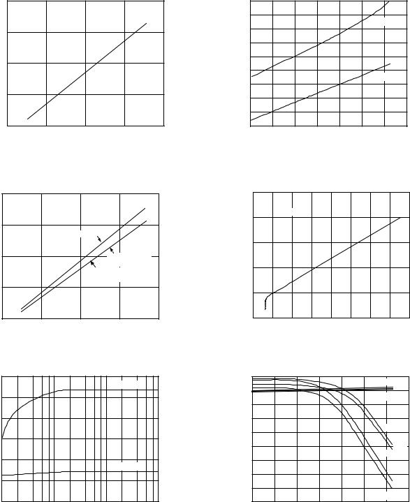
AD815–Typical Performance Characteristics
|
20 |
–6Volts |
|
RANGE |
15 |
|
|
VOLTAGE |
10 |
COMMON-MODE |
5 |
|
|
|
0 |
0 |
5 |
10 |
15 |
20 |
SUPPLY VOLTAGE –6Volts
Figure 1. Input Common-Mode Voltage Range vs. Supply
Voltage |
|
|
|
|
|
|
|
40 |
|
|
|
80 |
|
p-p |
|
|
|
|
|
p-p |
– V |
|
|
|
|
|
– V |
VOLTAGE |
30 |
|
|
|
60 |
VOLTAGE |
|
|
NO LOAD |
|
|||
|
|
|
|
|
||
OUTPUT |
20 |
|
|
RL = 50V |
40 |
OUTPUT |
|
|
|
(DIFFERENTIAL) |
|
||
|
|
|
RL = 25V |
|
||
SINGLE-ENDED |
|
|
|
|
DIFFERENTIAL |
|
|
|
|
(SINGLE-ENDED) |
|
||
10 |
|
|
|
20 |
||
|
|
|
|
|
||
|
0 |
|
|
|
0 |
|
|
0 |
5 |
10 |
15 |
20 |
|
SUPPLY VOLTAGE –6Volts
Figure 2. Output Voltage Swing vs. Supply Voltage
p-p |
30 |
|
|
60 |
p-p |
|
|
|
VS = 615V |
||
Volts |
25 |
|
|
50 |
Volts |
– |
|
|
|
|
– |
VOLTAGE |
20 |
|
|
40 |
VOLTAGE |
|
|
|
|
||
OUTPUT |
15 |
|
|
30 |
OUTPUT |
10 |
|
|
20 |
||
SINGLE-ENDED |
|
|
DIFFERENTIAL |
||
|
|
|
VS = 65V |
||
5 |
|
|
10 |
||
0 |
|
|
0 |
||
|
|
|
|
||
|
10 |
100 |
1k |
10k |
|
|
LOAD RESISTANCE – (Differential –V) (Single-Ended –V/2) |
|
|||
Figure 3. Output Voltage Swing vs. Load Resistance
|
36 |
|
|
|
|
|
|
|
|
34 |
|
|
|
|
|
VS = 615V |
|
|
|
|
|
|
|
|
|
|
– mA |
32 |
|
|
|
|
|
|
|
30 |
|
|
|
|
|
|
|
|
CURRENT |
28 |
|
|
|
|
|
|
|
26 |
|
|
|
|
|
|
|
|
SUPPLY |
|
|
|
|
|
|
VS = 65V |
|
24 |
|
|
|
|
|
|
|
|
22 |
|
|
|
|
|
|
|
|
|
|
|
|
|
|
|
|
|
|
20 |
|
|
|
|
|
|
|
|
18 |
|
|
|
|
|
|
|
|
–40 |
–20 |
0 |
20 |
40 |
60 |
80 |
100 |
|
|
|
JUNCTION TEMPERATURE –8C |
|
|
|||
Figure 4. Total Supply Current vs. Temperature
|
33 |
|
|
|
|
|
|
|
|
mA |
30 |
|
TA = +258C |
|
|
|
|
|
|
|
|
|
|
|
|
|
|
||
– |
|
|
|
|
|
|
|
|
|
CURRENT |
27 |
|
|
|
|
|
|
|
|
|
|
|
|
|
|
|
|
|
|
TOTAL SUPPLY |
24 |
|
|
|
|
|
|
|
|
21 |
|
|
|
|
|
|
|
|
|
|
18 |
|
|
|
|
|
|
|
|
|
0 |
2 |
4 |
6 |
8 |
10 |
12 |
14 |
16 |
SUPPLY VOLTAGE –6Volts
Figure 5. Total Supply Current vs. Supply Voltage
|
10 |
|
|
|
|
SIDE A, B |
|
|
|
0 |
|
|
|
|
+IB |
||
|
|
|
|
|
VS = 615V, 65V |
|||
|
|
|
|
|
|
|||
–mA |
–10 |
|
|
|
|
|
|
|
–20 |
|
|
|
|
|
|
|
|
CURRENT |
|
|
|
|
|
|
|
|
–30 |
|
|
|
|
|
VS = 65V |
||
|
|
|
|
|
SIDE B |
|||
|
|
|
|
|
|
|||
–40 |
|
|
|
|
|
|
–I |
|
|
|
|
|
|
|
|
||
BIAS |
|
|
|
|
|
|
B |
|
|
|
|
|
|
|
SIDE A |
||
–50 |
|
|
|
|
|
|
|
|
INPUT |
|
|
|
|
|
|
|
|
–60 |
|
|
|
|
|
SIDE B |
||
|
|
|
|
|
|
|
||
|
|
|
|
|
SIDE A |
|
||
|
|
|
|
|
|
–I |
||
|
–70 |
|
|
|
|
|
|
B |
|
|
|
|
|
|
|
|
|
|
–80 |
|
|
|
|
|
VS = 615V |
|
|
–20 |
0 |
20 |
40 |
60 |
80 |
100 |
|
|
–40 |
|||||||
|
|
|
JUNCTION TEMPERATURE –8C |
|
|
|||
Figure 6. Input Bias Current vs. Temperature
–4– |
REV. B |

|
|
|
|
|
|
|
|
|
|
|
|
|
|
|
|
|
AD815 |
|
|
0 |
|
|
|
|
|
|
|
|
80 |
|
|
|
|
|
|
|
|
|
|
|
|
|
|
|
|
|
|
TA = 258C |
|
|
|
|
|
|
|
|
mV |
–2 |
|
|
|
|
|
|
|
|
60 |
|
|
|
|
|
|
VS = |
|
|
|
|
|
|
|
|
|
|
|
|
|
|
|
|
|
|
||
|
|
|
|
|
|
|
|
|
|
|
|
|
|
|
|
615V |
|
|
VOLTAGEOFFSET– |
|
|
|
|
|
|
|
|
|
40 |
|
|
|
|
|
|
|
|
–4 |
|
|
|
|
|
|
|
mV–OFFSETRTI |
|
f = 0.1Hz 100V AD815 |
V |
|
||||||
|
|
|
|
|
VS = 65V |
|
|
|
|
|
||||||||
|
|
|
|
|
|
|
|
|
|
|
|
|
|
|
VS |
= |
|
|
|
–6 |
|
|
|
|
|
|
|
|
20 |
|
|
|
|
|
610V |
|
|
|
|
|
|
|
|
|
|
|
|
|
|
|
VS = |
|
|
|
||
|
|
|
|
|
|
|
|
|
|
|
|
|
|
|
|
|
|
|
|
–8 |
|
|
|
|
|
|
|
|
0 |
|
|
|
|
65V |
|
|
|
|
|
|
|
|
|
|
|
|
|
|
V I N |
|
|
|
|
|
||
|
|
|
|
|
|
|
|
|
|
|
|
|
1/2 |
|
|
|
||
|
|
|
|
|
|
|
|
|
|
|
|
|
|
|
|
|
||
INPUT |
–10 |
|
|
VS = 615V |
|
|
|
|
|
–20 |
|
|
|
49.9V |
|
OUT |
|
|
|
|
|
|
|
|
|
|
|
|
|
|
|
RL= |
|
||||
|
|
|
|
|
|
|
|
|
|
|
|
|
|
|
|
|||
|
–12 |
|
|
|
|
|
|
|
|
–40 |
|
|
|
|
|
|
|
|
|
|
|
|
|
|
|
|
|
|
|
|
1kV |
1kV |
5V |
|
|||
|
|
|
|
|
|
|
|
|
|
|
|
|
|
|
|
|||
|
–14 |
|
|
|
|
|
|
|
|
–60 |
|
|
0 |
|
|
|
|
|
|
–40 |
–20 |
0 |
20 |
40 |
60 |
80 |
100 |
|
–2.0 –1.6 |
–1.2 –0.8 |
–0.4 |
0.4 |
0.8 |
1.2 |
1.6 |
2.0 |
|
|
|
|
JUNCTION TEMPERATURE –8C |
|
|
|
|
LOAD CURRENT – Amps |
|
|
|
|||||||
Figure 7. Input Offset Voltage vs. Temperature
|
750 |
|
|
|
|
|
|
|
|
|
|
|
|
|
|
|
|
|
|
VS = 615V |
|
|
|
– mA |
700 |
|
|
|
|
|
|
|
|
|
|
|
|
SOURCE |
|
|
|
|
|
|
|
||
CURRENT |
650 |
|
|
|
|
|
|
|
|
||
|
|
|
|
|
|
|
|
|
|
||
600 |
|
|
|
|
|
|
|
|
|
|
|
CIRCUIT |
|
|
|
|
|
|
|
|
|
|
|
|
|
SINK |
|
|
|
|
|
|
|
|
|
550 |
|
|
|
|
|
|
|
|
|
|
|
SHORT |
|
|
|
|
|
|
|
|
|
|
|
500 |
|
|
|
|
|
|
|
|
|
|
|
|
|
|
|
|
|
|
|
|
|
|
|
|
450 |
|
|
|
|
|
|
|
|
|
|
|
–60 |
–40 |
–20 |
0 |
20 |
40 |
60 |
80 |
100 |
120 |
140 |
|
|
|
JUNCTION TEMPERATURE –8C |
|
|
|
|||||
Figure 8. Short Circuit Current vs. Temperature
|
15 |
|
|
|
|
|
|
|
|
|
|
10 |
TA = 258C |
|
|
|
VS = 610V |
|
|
||
|
RL = 25V |
|
|
|
|
|
|
|
||
|
|
|
VS = 65V |
|
|
|
|
|||
|
|
|
|
|
|
|
VS = 615V |
|||
mV |
5 |
|
|
|
|
|
|
|
|
|
– |
|
|
|
|
|
|
|
|
|
|
OFFSET |
0 |
|
|
|
|
|
|
|
|
|
|
|
|
|
|
V I N |
|
1/2 |
|
|
|
RTI |
|
|
|
|
|
|
|
|
||
–5 |
|
|
|
f = 0.1Hz |
100V |
AD815 |
VOUT |
|||
|
|
|
|
|
|
|
|
|
||
|
|
|
|
|
|
|
49.9V |
|
|
RL= |
|
–10 |
|
|
|
|
|
|
|
|
|
|
|
|
|
|
|
1kV |
1kV |
|
25V |
|
|
|
|
|
|
|
|
|
|
||
|
–15 |
|
|
|
|
|
|
|
|
|
|
–20 |
–16 |
–12 |
–8 |
–4 |
0 |
4 |
8 |
12 |
16 20 |
VOUT – Volts
Figure 9. Gain Nonlinearity vs. Output Voltage
Figure 10. Thermal Nonlinearity vs. Output Current Drive
–V |
100 |
|
|
|
|
|
|
|
|
|
|
|
|
|
|
|
|
|
|
RESISTANCE |
10 |
|
|
|
VS = 65V |
|
|
|
|
|
|
|
|
|
|
|
|||
|
|
|
|
|
|
|
|
|
|
OUTPUT |
1 |
|
|
|
|
|
VS = 615V |
|
|
|
|
|
|
|
|
|
|
|
|
CLOSED-LOOP |
0.1 |
|
|
|
|
|
|
|
|
0.01 |
|
|
|
|
|
|
|
|
|
|
30k |
100k |
300k |
1M |
3M |
10M |
30M |
100M |
300M |
FREQUENCY – Hz
Figure 11. Closed-Loop Output Resistance vs. Frequency
p-p |
40 |
|
|
|
|
TA = 258C |
|
|
|
|
|
|
VS = ±15V |
|
|
||
V |
|
|
|
|
|
|
|
|
– |
|
|
|
|
|
|
|
|
VOLTAGE |
|
|
|
RL = 100V |
|
|
|
|
30 |
|
|
|
|
|
|
|
|
|
|
|
|
|
|
|
|
|
OUTPUT |
|
|
|
RL = 50V |
|
|
|
|
20 |
|
|
|
|
|
|
|
|
|
|
|
|
|
|
|
|
|
DIFFERENTIAL |
|
|
|
RL = 25V |
|
|
|
|
10 |
|
|
|
|
|
|
|
|
|
|
|
RL = 1V |
|
|
|
|
|
|
|
|
|
|
|
|
|
|
|
0 |
|
|
|
|
|
|
|
|
0 |
2 |
4 |
6 |
8 |
10 |
12 |
14 |
|
|
|
|
FREQUENCY – MHz |
|
|
||
Figure 12. Large Signal Frequency Response
REV. B |
–5– |
 Loading...