


Analog Devices AD7821TQ, AD7821TE, AD7821KR, AD7821KP, AD7821BQ Datasheet
...
a |
LC2MOS High Speed, mP-Compatible |
|
8-Bit ADC with Track/Hold Function |
||
|
|
|
|
|
AD7821 |
|
|
|
|
FEATURES |
FUNCTIONAL BLOCK DIAGRAM |
|
Fast Conversion Time: 660 ns max |
|
|
100 kHz Track-and-Hold Function |
|
|
1 MHz Sample Rate |
|
|
Unipolar and Bipolar Input Ranges |
|
|
Ratiometric Reference Inputs |
|
|
No External Clock |
|
|
Extended Temperature Range Operation |
|
|
Skinny 20-Pin DlPs, SOIC and 20-Terminal |
|
|
Surface Mount Packages |
|
GENERAL DESCRIPTION
The AD7821 is a high speed, 8-bit, sampling, analog-to-digital converter that offers improved performance over the popular AD7820. It offers a conversion time of 660 ns (vs. 1.36 μs for the AD7820) and 100 kHz signal bandwidth (vs. 6.4 kHz). The sampling instant is better defined and occurs on the falling edge of WR or RD. The provision of a VSS pin (Pin 19) allows the part to operate from ±5 V supplies and to digitize bipolar input signals. Alternatively, for unipolar inputs, the VSS pin can be grounded and the AD7821 will operate from a single +5 V supply, like the AD7820.
The AD7821 has a built-in track-and-hold function capable of digitizing full-scale signals up to 100 kHz max. It also uses a half-flash conversion technique that eliminates the need to generate a CLK signal for the ADC.
The AD7821 is designed with standard microprocessor control signals (CS, RD, WR, RDY, INT) and latched, three-state data outputs capable of interfacing to high speed data buses. An overflow output (OFL) is also provided for cascading devices to achieve higher resolution.
The AD7821 is fabricated in Linear-Compatible CMOS (LC2MOS), an advanced, mixed technology process combining precision bipolar circuits with low power CMOS logic. The part features a low power dissipation of 50 mW.
REV. A
Information furnished by Analog Devices is believed to be accurate and reliable. However, no responsibility is assumed by Analog Devices for its use, nor for any infringements of patents or other rights of third parties which may result from its use. No license is granted by implication or otherwise under any patent or patent rights of Analog Devices.
PRODUCT HIGHLIGHTS
1. Fast Conversion Time
The half-flash conversion technique, coupled with fabrication on Analog Devices’ LC2MOS process, enables a very fast conversion time. The conversion time for the WR-RD mode is 660 ns, with 700 ns for the RD mode.
2. Built-In Track-and-Hold
This allows input signals with slew rates up to 1.6 V/μs to be converted to 8-bits without an external track-and-hold. This corresponds to a 5 V peak-to-peak, 100 kHz sine wave signal.
3. Total Unadjusted Error
The AD7821 features an excellent total unadjusted error figure of less than ±1 LSB over the full operating temperature range.
4. Unipolar/Bipolar Input Ranges
The AD7821 is specified for single supply (+5 V) operation with a unipolar full-scale range of 0 to +5 V, and for dual supply (±5 V) operation with a bipolar input range of ±2.5 V. Typical performance characteristics are given for other input ranges.
5. Dynamic Specifications for DSP Users
In addition to the traditional ADC specifications, the AD7821 is specified for ac parameters, including signal-to- noise ratio, distortion and slew rate.
One Technology Way, P.O. Box 9106, Norwood, MA 02062-9106, U.S.A. Tel: 617/329-4700 Fax: 617/326-8703
AD7821–SPECIFICATIONS |
VDD = +5 V 6 5%, GND = 0 V. Unipolar Input |
Range: VSS = GND, VREF(+) = 5 V, |
VREF(–) = GND. Bipolar Input Range: VSS = –5 |
V 6 5%, VREF(+) = 2.5 V, |
VREF(–) = –2.5 V. These test conditions apply unless otherwise stated. All specifications TMIN to TMAX unless otherwise noted. Specifications apply for RD Mode (Pin 7 = 0 V).
Parameter |
K Version1 |
B, T Versions |
Units |
Comments |
|||||||||||||||||||
UNIPOLAR INPUT RANGE |
|
|
|
|
|
|
|
|
|||||||||||||||
|
Resolution2 |
8 |
8 |
Bits |
|
|
|
|
|
||||||||||||||
|
Total Unadjusted Error3 |
± 1 |
± 1 |
LSB max |
|
|
|
|
|
||||||||||||||
|
Minimum Resolution for which |
|
|
|
|
|
|
|
|
||||||||||||||
|
No Missing Codes are Guaranteed |
8 |
8 |
Bits |
|
|
|
|
|
||||||||||||||
|
|
|
|
|
|
|
|
|
|
|
|
|
|
|
|
|
|
|
|
|
|
|
|
BIPOLAR INPUT RANGE |
|
|
|
|
|
|
|
|
|||||||||||||||
|
Resolution2 |
8 |
8 |
Bits |
|
|
|
|
|
||||||||||||||
|
Zero Code Error |
± 1 |
± 1 |
LSB max |
|
|
|
|
|
||||||||||||||
|
Full Scale Error |
± 1 |
± 1 |
LSB max |
|
|
|
|
|
||||||||||||||
|
Signal-to-Noise Ratio (SNR)3 |
45 |
45 |
dB min |
|
VIN = 99.85 kHz Full-Scale Sine Wave with fSAMPLING = 500 kHz |
|||||||||||||||||
|
Total Harmonic Distortion (THD)3 |
–50 |
–50 |
dB max |
|
VIN = 99.85 kHz Full-Scale Sine Wave with fSAMPLING = 500 kHz |
|||||||||||||||||
|
Peak Harmonic or Spurious Noise3 |
–50 |
–50 |
dB max |
|
VIN = 99.85 kHz Full-Scale Sine Wave with fSAMPLING = 500 kHz |
|||||||||||||||||
|
Intermodulation Distortion (IMD)3 |
|
|
|
|
fa (84.72 kHz) and fb (94.97 kHz) Full-Scale Sine Waves |
|||||||||||||||||
|
|
|
|
|
|
|
|
|
|
|
|
|
|
|
|
|
|
|
|
with fSAMPLING = 500 kHz |
|||
|
|
|
|
|
|
|
|
|
|
|
|
|
|
|
|
–50 |
–50 |
dB max |
Second Order Terms |
||||
|
|
|
|
|
|
|
|
|
|
|
|
|
|
|
|
–50 |
–50 |
dB max |
Third Order Terms |
||||
|
Slew Rate, Tracking3 |
1.6 |
1.6 |
V/μs max |
|
|
|
|
|
||||||||||||||
|
|
|
|
|
|
|
|
|
|
|
|
|
|
|
|
2.36 |
2.36 |
V/μs typ |
|
|
|
|
|
REFERENCE INPUT |
|
|
kΩ min/kΩ max |
|
|
|
|
|
|||||||||||||||
|
Input Resistance |
1.0/4.0 |
1.0/4.0 |
|
|
|
|
|
|||||||||||||||
|
VREF(+) Input Voltage Range |
VREF(–)/VDD |
VREF(–)/VDD |
V min/V max |
|
|
|
|
|
||||||||||||||
|
VREF(–) Input Voltage Range |
VSS/VREF(+) |
VSS/VREF(+) |
V min/V max |
|
|
|
|
|
||||||||||||||
ANALOG INPUT |
|
|
|
|
|
|
|
|
|||||||||||||||
|
Input Voltage Range |
VREF(–)/VREF(+) |
VREF(–)/VREF(+) |
V min/ max |
–5 V ≤ VIN ≤ +5 V |
||||||||||||||||||
|
Input Leakage Current |
± 3 |
± 3 |
μA max |
|||||||||||||||||||
|
Input Capacitance |
55 |
55 |
pF typ |
|
|
|
|
|
||||||||||||||
|
|
|
|
|
|
|
|
|
|
|
|
|
|
|
|
|
|
|
|
|
|
|
|
LOGIC INPUTS |
|
|
|
|
|
|
|
|
|||||||||||||||
|
CS |
, |
WR |
, |
RD |
|
|
|
|
|
|
|
|
|
|
|
|
|
|||||
|
VINH |
2.4 |
2.4 |
V min |
|
|
|
|
|
||||||||||||||
|
VINL |
0.8 |
0.8 |
V max |
|
|
|
|
|
||||||||||||||
|
IINH ( |
|
, |
|
|
) |
|
|
1 |
1 |
μA max |
|
|
|
|
|
|||||||
|
CS |
RD |
|
|
|
|
|
||||||||||||||||
|
IINH ( |
|
|
) |
|
|
|
3 |
3 |
μA max |
|
|
|
|
|
||||||||
|
WR |
|
|
|
|
|
|||||||||||||||||
|
IINL |
–1 |
–1 |
μA max |
|
|
|
|
|
||||||||||||||
|
Input Capacitance4 |
8 |
8 |
pF max |
|
Typically 5 pF |
|||||||||||||||||
|
MODE |
|
|
|
|
|
|
|
|
||||||||||||||
|
VINH |
3.5 |
3.5 |
V min |
|
|
|
|
|
||||||||||||||
|
VINL |
1.5 |
1.5 |
V max |
|
|
|
|
|
||||||||||||||
|
IINH |
200 |
200 |
μA max |
|
50 μA typ |
|||||||||||||||||
|
IINL |
–1 |
–1 |
μA max |
|
|
|
|
|
||||||||||||||
|
Input Capacitance4 |
8 |
8 |
pF max |
|
Typically 5 pF |
|||||||||||||||||
LOGIC OUTPUTS |
|
|
|
|
|
|
|
|
|||||||||||||||
|
DB0–DB7, |
OFL |
, |
INT |
|
|
|
|
|
ISOURCE = 360 μA |
|||||||||||||
|
VOH |
4.0 |
4.0 |
V min |
|
||||||||||||||||||
|
VOL |
0.4 |
0.4 |
V max |
|
ISINK = 1.6 mA |
|||||||||||||||||
|
IOUT (DB0–DB7) |
± 3 |
± 3 |
μA max |
|
Floating State Leakage |
|||||||||||||||||
|
Output Capacitance4 (DB0–DB7) |
8 |
8 |
pF max |
|
Typically 5 pF |
|||||||||||||||||
|
RDY |
|
|
|
|
|
|
|
|
||||||||||||||
|
VOL |
0.4 |
0.4 |
V max |
|
ISINK = 2.6 mA |
|||||||||||||||||
|
IOUT |
± 3 |
± 3 |
μA max |
|
Floating State Leakage |
|||||||||||||||||
|
Output Capacitance4 |
8 |
8 |
pF max |
|
Typically 5 pF |
|||||||||||||||||
POWER SUPPLY |
|
|
|
|
|
|
|
|
|||||||||||||||
|
IDD5 |
15 |
20 |
mA max |
|
CS |
= |
RD |
= 0 V |
||||||||||||||
ISS |
100 |
100 |
μA max |
|
|
= |
|
= 0 V |
|||||||||||||||
|
CS |
RD |
|||||||||||||||||||||
Power Dissipation |
50 |
50 |
mW typ |
|
|
|
|
|
|||||||||||||||
Power Supply Sensitivity |
± 1/4 |
± 1/4 |
LSB max |
± 1/16 LSB typ, VDD = 4.75 V to 5.25 V, |
|||||||||||||||||||
|
|
|
|
|
|
|
|
|
|
|
|
|
|
|
|
|
|
|
|
(VREF(+) = 4.75 V max for Unipolar Mode) |
|||
NOTES
1Temperature Ranges are as follows: K Version = –40°C to +85°C; B Version = –40°C to +85°C; T Version = –55°C to +125°C. 21 LSB = 19.53 mV for both the unipolar (0 V to +5 V) and bipolar (–2.5 V to +2.5 V) input ranges.
3See Terminology.
4Sample tested at +25°C to ensure compliance. 5See Typical Performance Characteristics.
Specifications subject to change without notice.
–2– |
REV. A |
AD7821
TIMING CHARACTERISTICS1 (VDD = +5 V ± 5%, VSS = 0 V or –5 V ± 5%; Unipolar or Bipolar Input Range)
|
|
Limit at |
Limit at |
|
|
|
|
|
|
|
|
|
|
|
|
|
|
Limit at +258C |
TMIN, TMAX |
TMIN, TMAX |
|
|
|
|
|
|
|
|
|
|
|
|
|
Parameter |
(All Versions) |
(K, B Versions) |
(T Version) |
Units |
|
Conditions/Comments |
||||||||||
|
|
|
|
|
|
|
|
|
|
|
|
|
|
|
|
|
tCSS |
0 |
0 |
0 |
ns min |
|
|
|
to |
|
/ |
|
Setup Time |
||||
|
CS |
RD |
WR |
|||||||||||||
tCSH |
0 |
0 |
0 |
ns min |
|
CS to RD/WR Hold Time |
||||||||||
2 |
70 |
85 |
100 |
ns max |
|
CS to RDY Delay. Pull-Up |
||||||||||
tRDY |
|
|||||||||||||||
|
|
|
|
|
|
Resistor 5 k1. |
||||||||||
tCRD |
700 |
875 |
975 |
ns max |
Conversion Time (RD Mode) |
|||||||||||
3 |
|
|
|
|
|
Data Access Time (RD Mode) |
||||||||||
tACC0 |
|
|
|
|
|
|||||||||||
|
tCRD + 25 |
tCRD + 30 |
tCRD + 35 |
ns max |
CL = 20 pF |
|||||||||||
2 |
tCRD + 50 |
tCRD + 65 |
tCRD + 75 |
ns max |
CL = 100 pF |
|||||||||||
50 |
– |
– |
ns typ |
|
RD to INT Delay (RD Mode) |
|||||||||||
tINTH |
|
|||||||||||||||
tDH4 |
80 |
85 |
90 |
ns max |
|
|
|
|
|
|
|
|
|
|
|
|
15 |
15 |
15 |
ns min |
Data Hold Time |
||||||||||||
|
60 |
70 |
80 |
ns max |
|
|
|
|
|
|
|
|
|
|
|
|
tP |
350 |
425 |
500 |
ns min |
Delay Time Between Conversions |
|||||||||||
tWR |
250 |
325 |
400 |
ns min |
Write Pulse Width |
|||||||||||
|
10 |
10 |
10 |
μs max |
|
|
|
|
|
|
|
|
|
|
|
|
tRD |
250 |
350 |
450 |
ns min |
Delay Time between |
WR |
and |
RD |
Pulses |
|||||||
tREAD1 |
160 |
205 |
240 |
ns min |
|
RD Pulse Width (WR-RD Mode, see Figure 12b) |
||||||||||
3 |
|
|
|
|
|
Determined by tACC1 |
||||||||||
|
|
|
|
|
Data Access Time (WR-RD Mode, see Figure 12b) |
|||||||||||
tACC1 |
|
|
|
|
|
|||||||||||
|
160 |
205 |
240 |
ns max |
CL = 20 pF |
|||||||||||
|
185 |
235 |
275 |
ns max |
CL = 100 pF |
|||||||||||
tRI |
150 |
185 |
220 |
ns max |
|
RD to INT Delay |
||||||||||
2 |
380 |
– |
– |
ns typ |
|
WR to INT Delay |
||||||||||
tINTL |
|
|||||||||||||||
|
500 |
610 |
700 |
ns max |
|
|
|
|
|
|
|
|
|
|
|
|
tREAD2 |
65 |
75 |
85 |
ns min |
|
RD |
Pulse Width (WR-RD Mode, see Figure 12a) |
|||||||||
|
|
|
|
|
|
Determined by tACC2 |
||||||||||
3 |
|
|
|
|
|
Data Access Time (WR-RD Mode, see Figure 12a) |
||||||||||
65 |
75 |
85 |
ns max |
|
CL = 20 pF |
|||||||||||
tACC2 |
|
|||||||||||||||
2 |
90 |
110 |
130 |
ns max |
CL = 100 pF |
|||||||||||
80 |
100 |
120 |
ns max |
|
WR to INT Delay (Stand-Alone Operation) |
|||||||||||
tIHWR |
|
|||||||||||||||
tID3 |
|
|
|
|
|
Data Access Time after INT |
||||||||||
|
|
|
|
|
|
(Stand-Alone Operation) |
||||||||||
|
30 |
35 |
40 |
ns max |
|
CL = 20 pF |
||||||||||
|
45 |
60 |
70 |
ns max |
|
CL = 100 pF |
||||||||||
NOTES
1Sample tested at +25°C to ensure compliance. All input control signals are specified with tr = tf = 5 ns (10% to 90% of +5 V) and timed from a voltage level of 1.6 V.
2CL = 50 pF.
3Measured with load circuits of Figure 1 and defined as the time required for an output to cross 0.8 V or 2.4 V. 4Defined as the time required for the data lines to change 0.5 V when loaded with the circuits of Figure 2.
Specifications subject to change without notice.
Test Circuits
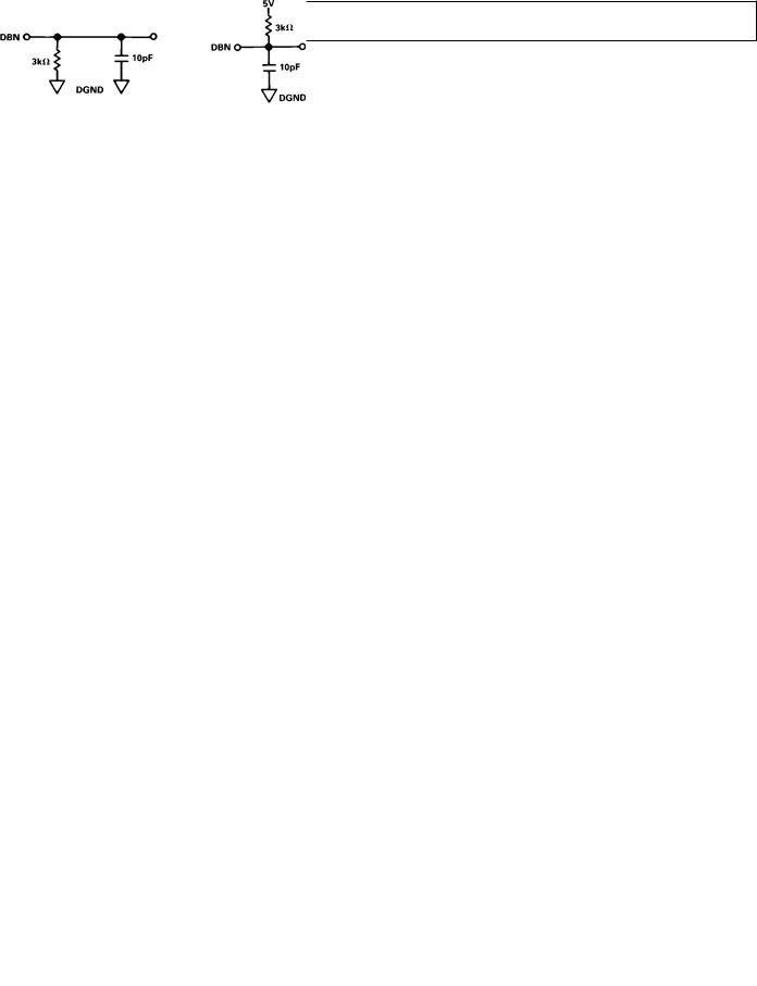
a. High Z to VOH b. High Z to VOL Figure 1. Load Circuits for Data Access Time Test
ORDERING GUIDE
|
|
Total |
|
|
Temperature |
Unadjusted |
Package |
Model1 |
Range |
Error (LSB) |
Option2 |
AD7821KN |
–40°C to +85°C |
±1 max |
N-20 |
AD7821KP |
–40°C to +85°C |
±1 max |
P-20A |
AD7821KR |
–40°C to +85°C |
±1 max |
R-20 |
AD7821BQ |
–40°C to +85°C |
±1 max |
Q-20 |
AD7821TQ |
–55°C to +125°C |
±1 max |
Q-20 |
AD7821TE |
–55°C to +125°C |
±1 max |
E-20A |
|
|
|
|
NOTES
1To order MIL-STD-883, Class B processed parts, add /883B to part number. Contact local sales office for military data sheet.
2E = Leadless Ceramic Chip Carrier; N = Plastic DIP; P = Plastic Leaded Chip Carrier; Q = Cerdip; R = SOIC.
a. VOH to High Z b. VOL to High Z Figure 2. Load Circuits for Data Hold Time Test
REV. A |
–3– |

AD7821
ABSOLUTE MAXIMUM RATINGS* |
Industrial (B Version) . |
. |
. . . |
. . . . . . . . . . |
. –40°C to +85°C |
|||
VDD to GND . . . . . . . . . . . . . |
. . . . . . . . . . . . . . –0.3 V, + 7 V |
Extended (T Version) . |
. . . . . . . . . . . . . . –55°C to +125°C |
|||||
VSS to GND . . . . . . . . . . . . . . |
. . . . . . . . . . . . . . +0.3 V, + 7 V |
Storage Temperature Range . . . . . . . . . . . . |
–65°C to +150°C |
|||||
Digital Input Voltage to GND |
|
Lead Temperature (Soldering, 10 secs) . . . . |
. . . . . . . +300°C |
|||||
(Pins 6–8, 13) . . . . . . . . . . |
. . . . . . . . . –0.3 V, VDD + 0.3 V |
Power Dissipation (Any Package) to +75°C . |
. . . . . . . 450 mW |
|||||
Digital Output Voltage to GND |
Derates above +75°C by . |
. |
. . . |
. . . . . . . . . . |
. . . . . . 6 mW/°C |
|||
(Pins 2–5, 9, 14–18) . . . . . |
. . . . . . . . . . –0.3 V, VDD + 0.3 V |
*Stresses above those listed under “Absolute Maximum Ratings” may cause |
||||||
VREF(+) to GND . . . . . . . . . . . . . . . VSS – 0.3 V, VDD + 0.3 V |
permanent damage to the device. This is a stress rating only and functional |
|||||||
VREF(–) to GND . . . . . . . . . . . . . . . VSS – 0.3 V, VDD + 0.3 V |
operation of the device at these or any other conditions above those indicated in the |
|||||||
VIN to GND |
VSS – 0.3 V, VDD + 0.3 V |
operational sections of this specification is not implied. Exposure to absolute |
||||||
maximum rating conditions for extended periods may affect device reliability. |
||||||||
Operating Temperature Range |
||||||||
|
|
|
|
|
||||
Commercial (K Version) . |
. . . . . . . . . . . . . –40°C to +85°C |
|
|
|
|
|
||
CAUTION |
|
|
|
|
|
|
|
|
|
|
|
|
|
|
|
||
ESD (electrostatic discharge) sensitive device. Electrostatic charges as high as 4000 V readily |
|
|
|
|
||||
|
|
WARNING! |
||||||
accumulate on the human body and test equipment and can discharge without detection. |
|
|
||||||
Although the AD7821 features proprietary ESD protection circuitry, permanent damage may |
|
|
|
|
||||
occur on devices subjected to high energy electrostatic discharges. Therefore, proper ESD |
|
|
|
ESD SENSITIVE DEVICE |
||||
precautions are recommended to avoid performance degradation or loss of functionality. |
|
|
|
|||||
|
|
|
|
|||||
|
|
|
|
|
|
|
||
|
|
PIN CONFIGURATIONS |
|
|
|
|
||
DIP AND SOIC |
LCCC |
|
|
|
PLCC |
|||
TERMINOLOGY
LEAST SIGNIFICANT BIT (LSB)
An ADC with 8-bit resolution can resolve one part in 28 (1/256 of full scale). For the AD7821 operating in either the unipolar or bipolar input range with 5 V full scale, one LSB is 19.53 mV.
TOTAL UNADJUSTED ERROR
This is a comprehensive specification which includes relative accuracy, offset error and full-scale error.
SLEW RATE
Slew Rate is the maximum allowable rate of change of input signal such that the digital sample values are not in error.
TOTAL HARMONIC DISTORTION
Total harmonic distortion is the ratio of the square root of the sum of the squares of the rms value of the harmonics to the rms value of the fundamental. For the AD7821, total harmonic distortion (THD) is defined as
é |
2 |
2 |
2 |
2 |
ù |
|
ê |
(V2 |
+V3 |
+V5 |
+V6 |
)ú |
|
20 log ê |
|
|
|
|
|
údB |
|
V1 |
|
|
|||
ê |
|
|
ú |
|||
ê |
|
|
|
|
ú |
|
ë |
|
|
|
|
û |
|
where V1 is the rms amplitude of the fundamental and V2, V3, V4, V5, V6, are the rms amplitudes of the individual harmonics.
INTERMODULATION DISTORTION
With inputs consisting of sine waves at two frequencies, fa and fb, any active device with nonlinearities will create distortion products, of order (m+n), at sum and difference frequencies of mfa+nfb, where m, n = 0, 1, 2, 3,- - - -. Intermodulation terms are those for which m or n is not equal to zero. For example, the second order terms include (fa + fb) and (fa – fb), and the third order terms include (2fa + fb), (2fa – fb), (fa + 2fb) and
(fa – 2fb). For the AD7821 intermodulation distortion is calculated separately for both the second and third order terms.
SIGNAL-TO-NOISE RATIO
Signal-to-noise ratio (SNR) is measured signal-to-noise at the output of the ADC. The signal is the rms magnitude of the fundamental. Noise is the rms sum of all nonfundamental signals (excluding dc) up to half the sampling frequency. SNR is dependent on the number of quantization levels used in the digitization process. The theoretical SNR for a sine wave input is given by:
SNR = (6.02 N + 1.76) dB
where N is the number of bits in the ADC. Thus, for an ideal 8-bit ADC, SNR = 50 dB.
PEAK HARMONIC OR SPURIOUS NOISE
Peak harmonic or spurious noise is the rms value of the largest nonfundamental frequency (excluding dc) up to half the sampling frequency to the rms value of the fundamental.
–4– |
REV. A |
 Loading...