


AD7834AR
Table of contents
 Loading...
Analog Devices AD7834AR, AD7834AN, AD7835BS, AD7835AS, AD7835AP Datasheet
...
LC2MOS
X1
DAC 1
LATCH
INPUT
REGISTER
1
VCCVDDV
SS
V
REF
(–)A
V
REF
(+)A
V
OUT
1
BYSHF
DB13
DB0
A0
A1
A2
CS
X1
DAC 2
LATCH
DAC 2
INPUT
REGISTER
2
X1
DAC 3
LATCH
INPUT
REGISTER
3
X1
DAC 4
LATCH
INPUT
REGISTER
4
DAC 1
AD7835
V
OUT
2
V
OUT
3
V
OUT
4
AGND
DGND
LDAC
DSG B
CLR
DSG A
DAC 4
DAC 3
V
REF
(–)B
V
REF
(+)B
ADDRESS
DECODE
INPUT
BUFFER
WR
14
a
FEATURES
Four 14-Bit DACs in One Package
AD7834—Serial Loading
AD7835—Parallel 8-/14-Bit Loading
Voltage Outputs
Power-On Reset Function
Max/Min Output Voltage Range of +/–8.192 V
Maximum Output Voltage Span of 14 V
Common Voltage Reference Inputs
User Assigned Device Addressing
Clear Function to User-Defined Voltage
Surface Mount Packages
AD7834—28-Pin SO, DIP and Cerdip
AD7835—44-Pin PQFP and PLCC
APPLICATIONS
Process Control
Automatic Test Equipment
General Purpose Instrumentation
Quad 14-Bit DAC
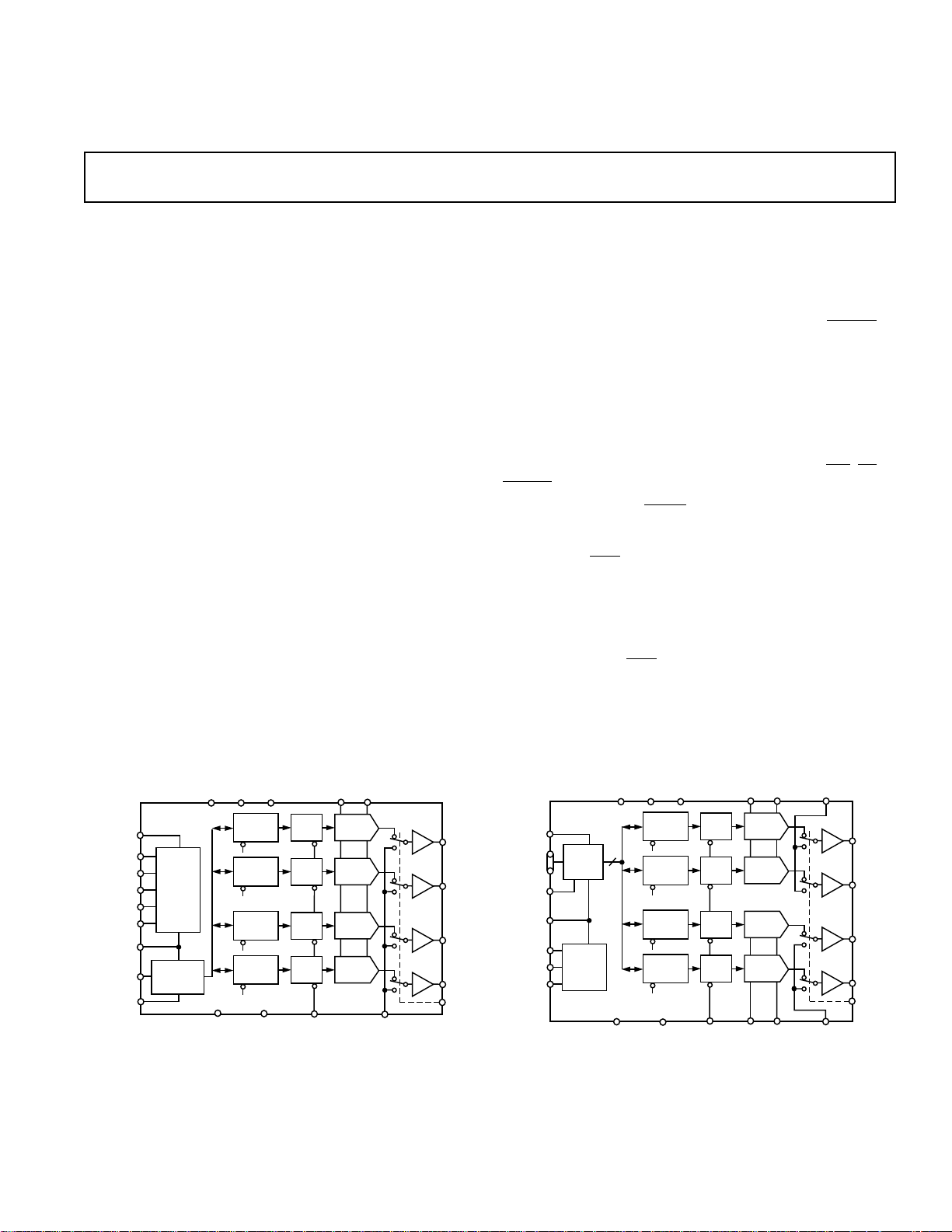
AD7834/AD7835
GENERAL DESCRIPTION
The AD7834 and AD7835 contain four 14-bit DACs on one
monolithic chip. The AD7834 and AD7835 have output voltages in the range of ±8.192 V with a maximum span of 14 V.
The AD7834 is a serial input device. Data is loaded in 16-bit
format from the external serial bus, MSB first after two leading
0s, into one of the input latches via DIN, SCLK and
The AD7834 has five dedicated package address pins, PA0–
PA4, that can be wired to AGND or V
to permit up to 32
CC
AD7834s to be individually addressed in a multipackage
application.
The AD7835 can accept either 14-bit parallel loading or
double-byte loading, where right-justified data is loaded in one
8-bit and one 6-bit byte. Data is loaded from the external bus
into one of the input latches under the control of the
BYSHF and DAC channel address pins, A0–A2.
With either device, the
LDAC signal can be used to update
either all four DAC outputs simultaneously or individually,
on reception of new data. In addition, for either device, the
asynchronous
V
1–V
OUT
CLR input can be used to set all signal outputs,
4, to the user-defined voltage level on the Device
OUT
Sense Ground pin, DSG. On power-on, before the power supplies have stabilized, internal circuitry holds the DAC output
voltage levels to within ±2 V of the DSG potential. As the supplies stabilize, the DAC output levels move to the exact DSG
potential (assuming
CLR is exercised).
The AD7834 is available in 28-pin 0.3" SO and 0.6" DIP packages, and the AD7835 is available in a 44-pin PQFP package
and a 44-pin PLCC package.
FSYNC.
WR, CS,
AD7834 FUNCTIONAL BLOCK DIAGRAM
V
VDDV
CC
PA0
PA1
PA2
PA3
PA4
DIN
SCLK
AD7834
CONTROL
ADDRESS
DECODE
SERIAL-TOPARALLEL
CONVERTER
LOGIC
&
AGND
PAEN
FSYNC
REV. A
Information furnished by Analog Devices is believed to be accurate and
reliable. However, no responsibility is assumed by Analog Devices for its
use, nor for any infringements of patents or other rights of third parties
which may result from its use. No license is granted by implication or
otherwise under any patent or patent rights of Analog Devices.
REGISTER
REGISTER
REGISTER
REGISTER
INPUT
1
INPUT
2
INPUT
3
INPUT
4
DGND
SS
DAC 1
LATCH
DAC 2
LATCH
DAC 3
LATCH
DAC 4
LATCH
LDAC
V
(–)
(+)
V
REF
REF
DAC 1
DAC 2
DAC 3
DAC 4
DSG
X1
X1
X1
X1
V
V
V
V
CLR
OUT
OUT
OUT
OUT
1
2
3
4
One Technology Way, P.O. Box 9106, Norwood. MA 02062-9106, U.S.A.
Tel: 617/329-4700 Fax: 617/326-8703
AD7835 FUNCTIONAL BLOCK DIAGRAM
© Analog Devices, Inc., 1995
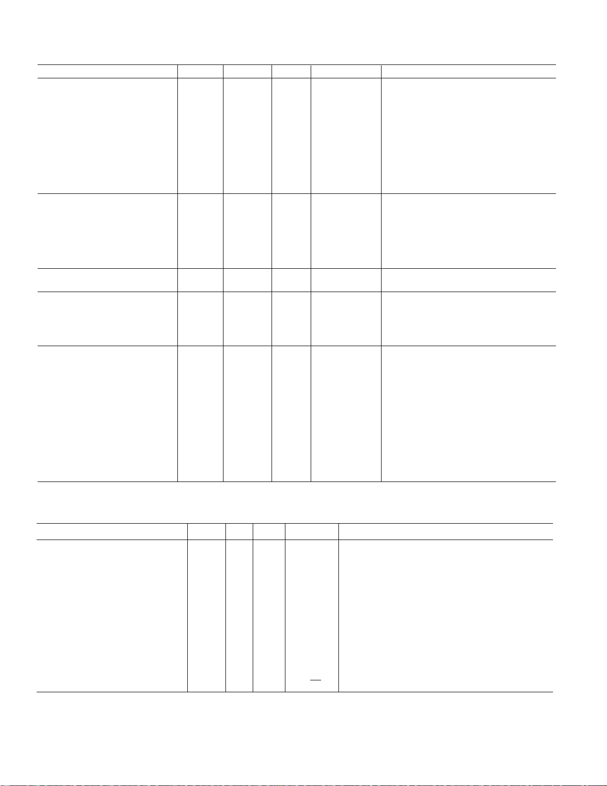
(VCC = +5 V ± 5%; VDD = +15 V ± 5%; VSS = –15 V ± 5%; AGND =
AD7834/AD7835–SPECIFICATIONS
P
arameter A B S Units Test Conditions/Comments
DGND = 0 V; T
ACCURACY
Resolution 14 14 14 Bits
Relative Accuracy ±2 ±1 ±2 LSB max
Differential Nonlinearity ±0.9 ±0.9 ±0.9 LSB max Guaranteed Monotonic Over Temperature
Full-Scale Error V
to T
T
MIN
MAX
±5 ±5 ±8 mV max
Zero-Scale Error ±4 ±4 ±5 mV max V
Gain Error ±0.5 ±0.5 ±0.5 mV typ V
Gain Temperature Coefficient
DC Crosstalk
2
2
4 4 4 ppm FSR/°C typ
20 20 20 ppm FSR/°C max
50 50 50 µV max See Terminology. RL = 10 kΩ
REFERENCE INPUTS
DC Input Resistance 30 30 30 MΩ typ
Input Current ±1 ±1 ±1 µA max Per Input
(+) Range 0/+8.192 +7/+8.192 0/+8.192 V min/max
V
REF
(–) Range –8.192/0 –8.192/0 –8.192/0 V min/max
V
REF
[V
REF
(+)–V
(–)] 5/14 7/14 5/14 V min/max For Specified Performance. Can Go as Low as
REF
DEVICE SENSE GROUND INPUTS
Input Current ±2 ±2 ±2 µA max Per Input. V
DIGITAL INPUTS
, Input High Voltage 2.4 2.4 2.4 V min
V
INH
, Input Low Voltage 0.8 0.8 0.8 V max
V
INL
, Input Current ±10 ± 10 ±10 µA max
I
INH
CIN, Input Capacitance 10 10 10 pF max
POWER REQUIREMENTS
V
CC
V
DD
V
SS
5.0 5.0 5.0 V nom ±5% for Specified Performance
15.0 15.0 15.0 V nom ±5% for Specified Performance
–15.0 –15.0 –15.0 V nom ± 5% for Specified Performance
Power Supply Sensitivity
∆Full Scale/∆V
∆Full Scale/∆V
I
CC
DD
SS
110 110 110 dB typ
100 100 100 dB typ
0.2 0.2 0.5 mA max V
3 3 3 mA max AD7834. V
6 6 6 mA max AD7835. V
I
DD
10 10 15 mA max AD7834. Outputs Unloaded
15 15 15 mA max AD7835. Outputs Unloaded
I
SS
10 10 15 mA max Outputs Unloaded
1
= T
to T
A
MIN
, unless otherwise noted)
MAX
(+) = +7 V, V
REF
(+) = +7 V, V
REF
(+) = +7 V, V
REF
(–) = –7 V
REF
(–) = –7 V
REF
(–) = –7 V
REF
0 V, but Performance Not Guaranteed
= –2 V to +2 V
DSG
= VCC, V
INH
= DGND
INL
= 2.4 V min, V
INH
= 2.4 V min, V
INH
= 0.8 V max
INL
= 0.8 V max
INL
(These characteristics are included for Design Guidance and are not
AC PERFORMANCE CHARACTERISTICS
P
arameter A B S Units Test Conditions/Comments
DYNAMIC PERFORMANCE
Output Voltage Settling Time 10 10 10 µs typ Full-Scale Change to ±1/2 LSB. DAC Latch Contents
Digital-to-Analog Glitch Impulse 120 120 120 nV-s typ Measured with V
DC Output Impedance 0.5 0.5 0.5 Ω typ See Terminology
Channel-to-Channel Isolation 100 100 100 dB typ See Terminology; Applies to the AD7835 Only
DAC to DAC Crosstalk 25 25 25 nV-s typ See Terminology
Digital Crosstalk 3 3 3 nV-s typ Feedthrough to DAC Output Under Test Due to
Digital Feedthrough – AD7834 0.2 0.2 0.2 nV-s typ Effect of Input Bus Activity on DAC Output Under Test
Digital Feedthrough – AD7834 0.1 0.1 0.1 nV-s typ
Output Noise Spectral Density
@ 1 kHz 40 40 40 nV/√Hz typ All 1s Loaded to DAC. V
NOTES
1
Temperature range is as follows: A Version: –40°C to +85°C; B Version: –40°C to +85°C; S Version: –55°C to +125°C.
2
Guaranteed by design.
Specifications subject to change without notice
subject to production testing. )
Alternately Loaded with All 0s and All 1s
Alternately Loaded with All 0s and All 1s
Change in Digital Input Code to Another Converter
–2–
REF
(+) = V
REF
(–) = 0 V. DAC Latch
REF
(+) = V
(–) = 0 V
REF
REV. A
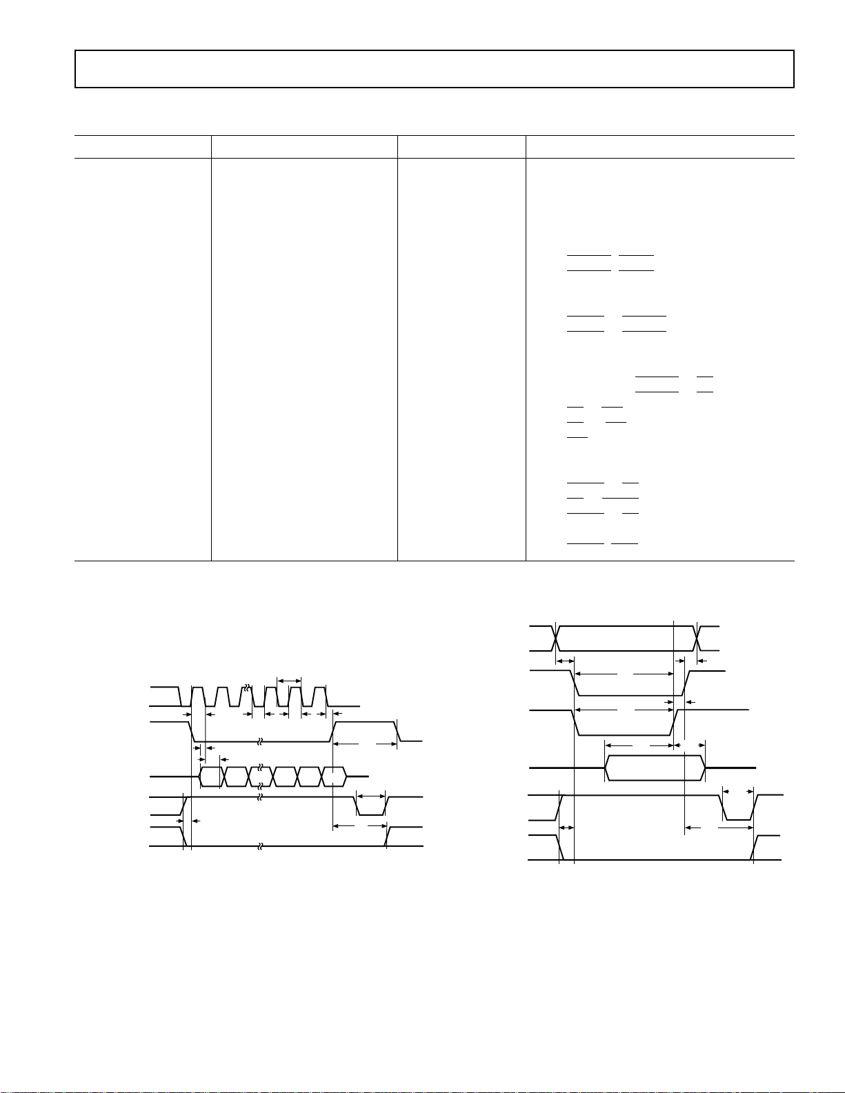
TIMING SPECIFICATIONS
t
12
t
14
t
17
t
16
t
15
t
10
t
18
t
19
t
11
t
13
A0. A1 A2
BYSHF
CS
WR
DATA
LDAC
(SIMULTANEOUS
UPDATE)
LDAC
(PRE-CHANNEL
UPDATE)
AD7834/AD7835
1
(VCC = +5 V ± 5%; VDD = +15 V ± 5%; VSS = –15 V ± 5%; AGND = DGND = 0 V)
Parameter Limit at T
AD7834 Specific
2
t
1
2
t
2
100 ns min SCLK Cycle Time
50 ns min SCLK Low Time @ +25°C
MIN, TMAX
Units Description
60 ns min SCLK Low Time –40°C to +85°C
2
t
3
t
4
t
5
t
6
t
7
t
8
t
9
t
21
66 ns min SCLK Low Time –55°C to +125°C
30 ns min SCLK High Time
30 ns min FSYNC, PAEN Setup Time
40 ns min FSYNC, PAEN Hold Time
30 ns min Data Setup Time
10 ns min Data Hold Time
0 ns min LDAC to FSYNC Setup Time
40 ns min LDAC to FSYNC Hold Time
20 ns min Delay Between Write Operations
AD7835 Specific
t
11
t
12
t
13
t
14
t
15
t
16
t
17
t
18
t
19
t
20
15 ns min A0, A1, A2, BYSHF to CS Setup Time
15 ns min A0, A1, A2, BYSHF to CS Hold Time
0 ns min CS to WR Setup Time
0 ns min CS to WR Hold Time
40 ns min WR Pulse Width
40 ns min Data Setup Time
10 ns min Data Hold Time
0 ns min LDAC to CS Setup Time
0 ns min CS to LDAC Setup Time
0 ns min LDAC to CS Hold Time
General
t
10
NOTES
1
All input signals are specified with tr = tf = 5 ns (10% to 90% of 5 V) and timed from a voltage level of 1.6 V.
2
Rise and fall times should be no longer than 50 ns.
Specifications subject to change without notice.
40 ns min LDAC, CLR Pulse Width
FSYNC
(SIMULTANEOUS
LDAC
UPDATE)
LDAC
(PRE-CHANNEL
UPDATE)
REV. A
1ST
2ND
CLK
CLK
SCLK
t
4
t
6
t
7
DIN
Figure 1. AD7834 Timing Diagram
D0 D1
t
8
t
1
t
t
2
24TH
CLK
D23
t
5
t
20
t
10
t
9
3
D22
Figure 2. AD7835 Timing Diagram
–3–
AD7834/AD7835
WARNING!
ESD SENSITIVE DEVICE
ABSOLUTE MAXIMUM RATINGS
(TA = +25°C unless otherwise noted)
VCC to DGND . . . . . . . . . . . . . . . –0.3 V, +7 V or V
V
to AGND . . . . . . . . . . . . . . . . . . . . . . . . . . –0.3 V, +17 V
DD
V
to AGND . . . . . . . . . . . . . . . . . . . . . . . . . . +0.3 V, –17 V
SS
AGND to DGND . . . . . . . . . . . . . . . . . . . . . . . –0.3 V, +0.3 V
Digital Inputs to DGND . . . . . . . . . . . . . . –0.3 V, V
V
(+) to V
REF
V
(+) to AGND . . . . . . . . . . . . . . . V
REF
V
(–) to AGND . . . . . . . . . . . . . . . V
REF
(–) . . . . . . . . . . . . . . . . . . . . . . . –0.3 V, +18 V
REF
DSG to AGND . . . . . . . . . . . . . . . . . V
V
(1–4) to AGND . . . . . . . . . . . . V
OUT
Operating Temperature Range
Industrial (A Version) . . . . . . . . . . . . . . . . .–40°C to +85°C
Extended (S Version). . . . . . . . . . . . . . . . . –55°C to +125°C
Storage Temperature Range . . . . . . . . . . . . .–65°C to +150°C
Junction Temperature . . . . . . . . . . . . . . . . . . . . . . . . . +150°C
Plastic Package
θ
Thermal Impedance . . . . . . . . . . . . . . . . . . . . . +75°C/W
JA
Lead Temperature, Soldering (10 sec) . . . . . . . . . . . +260°C
Cerdip Package
θ
Thermal Impedance . . . . . . . . . . . . . . . . . . . . . +52°C/W
JA
Lead Temperature, Soldering (10 sec) . . . . . . . . . . . +300°C
1
DD
(Whichever Is Lower)
CC
– 0.3 V, VDD + 0.3 V
SS
– 0.3 V, VDD + 0.3 V
SS
– 0.3 V, VDD + 0.3 V
SS
– 0.3 V, VDD + 0.3 V
SS
+ 0.3 V
+ 0.3 V
SOIC Package
θ
Thermal Impedance . . . . . . . . . . . . . . . . . . . . . +75°C/W
JA
Lead Temperature, Soldering
Vapor Phase (60 sec) . . . . . . . . . . . . . . . . . . . . . . +215°C
Infrared (15 sec) . . . . . . . . . . . . . . . . . . . . . . . . . . +220°C
PQFP Package
θ
Thermal Impedance . . . . . . . . . . . . . . . . . . . . . . 95°C/W
JA
Lead Temperature, Soldering
Vapor Phase (60 sec) . . . . . . . . . . . . . . . . . . . . . . +215°C
Infrared (15 sec) . . . . . . . . . . . . . . . . . . . . . . . . . . +220°C
PLCC Package
θ
Thermal Impedance. . . . . . . . . . . . . . . . . . . . . . +55°C/W
JA
Lead Temperature, Soldering
Vapor Phase (60 sec) . . . . . . . . . . . . . . . . . . . . . . +215°C
Infrared (15 sec) . . . . . . . . . . . . . . . . . . . . . . . . . . +220°C
Power Dissipation (Any Package) . . . . . . . . . . . . . . . .480 mW
NOTES
1
Stresses above those listed under “Absolute Maximum Ratings” may cause
permanent damage to the device. This is a stress rating only and functional
operation of the device at these or any other conditions above those indicated in the
operational section of this specification is not implied. Exposure to absolute
maximum rating conditions for extended periods may affect device reliability.
2
Transient currents of up to 100 mA will not cause SCR latch up.
CAUTION
ESD (electrostatic discharge) sensitive device. Electrostatic charges as high as 4000 V readily
accumulate on the human body and test equipment and can discharge without detection.
Although the AD7834/AD7835 feature proprietary ESD protection circuitry, permanent damage
may occur on devices subjected to high energy electrostatic discharges. Therefore, proper ESD
precautions are recommended to avoid performance degradation or loss of functionality.
ORDERING GUIDE
Linearity
Temperature Error DNL Package
Model Range (LSBs) (LSBs) Option
AD7834AR –40°C to +85°C ±2 ±0.9 R-28
AD7834BR –40°C to +85°C ±1 ±0.9 R-28
AD7834AN –40°C to +85°C ±2 ± 0.9 N-28
AD7834BN –40°C to +85°C ±1 ±0.9 N-28
AD7834SQ –55°C to +125°C ±2 ± 0.9 Q-28
AD7835AS
AD7835BS
AD7835AP
NOTES
1
R = Small Outline IC (SOIC); N = Plastic DIP; Q = Cerdip; S = Plastic Quad Flatpack (PQFP);
P = Plastic Leaded Chip Carrier (PLCC).
2
Contact Sales Office for availability.
2
2
2
–40°C to +85°C ±2 ± 0.9 S-44
–40°C to +85°C ±1 ± 0.9 S-44
–40°C to +85°C ±2 ± 0.9 P-44A
1
–4–
REV. A
Pin Mnemonic Description
AD7834/AD7835
AD7834 PIN DESCRIPTION
V
CC
V
SS
V
DD
Logic Power Supply; +5 V ± 5%.
Negative Analog Power Supply; –15 V ± 5%.
Positive Analog Power Supply; +15 V ± 5%.
DGND Digital Ground.
AGND Analog Ground.
(+) Positive Reference Input. The positive reference voltage is referred to AGND.
V
REF
(–) Negative Reference Input. The negative reference voltage is referred to AGND.
V
REF
1...V
V
OUT
DSG Device Sense Ground Input. Used in conjunction with the
4 DAC Outputs.
OUT
When
CLR input for power-on protection of the DACs.
CLR is low, the DAC outputs are forced to the potential on the DSG pin.
DIN Serial Data Input.
SCLK Clock input for writing data to the device.
FSYNC Frame Sync Input. Active low logic input used, in conjunction with DIN and SCLK, to write data to the device
with serial data expected after the falling edge of this signal. The contents of the 24-bit serial-to-parallel input
register are transferred on the rising edge of this signal.
PA0 . . . PA4 Package Address Inputs. These inputs are hardwired high (V
) or low (DGND) to assign dedicated package
CC
addresses in a multipackage environment.
PAEN Package Address Enable Input. When low, this input allows normal operation of the device. When it is high, the
device ignores the package address (but not the channel address) in the serial data stream and loads the serial
data into the input registers. This feature is useful in a multipackage application where it can be used to load the
same data into the same channel in each package.
LDAC Load DAC Input (level sensitive). This input signal in conjunction with the FSYNC input signal, determines
how the analog outputs are updated. If
device’s input registers, no change occurs on the analog outputs. Subsequently, when
LDAC is maintained high while new data is being loaded into the
LDAC is brought low, the
contents of all four input registers are transferred into their respective DAC latches, updating the analog outputs.
Alternatively, if
corresponding analog output) is updated immediately on the rising edge of
LDAC is kept low while new data is shifted into the device, then the addressed DAC latch (and
FSYNC.
CLR Asynchronous Clear Input (level sensitive, active low). When this input is brought low, all analog outputs are
switched to the externally set potential on the DSG pin. When
the DSG potential until
LDAC is brought low. When LDAC is brought low, the analog outputs are switched
back to reflect their individual DAC output levels. As long as
CLR is brought high, the signal outputs remain at
CLR remains low, the LDAC signals are ignored
and the signal outputs remain switched to the potential on the DSG pin.
REV. A
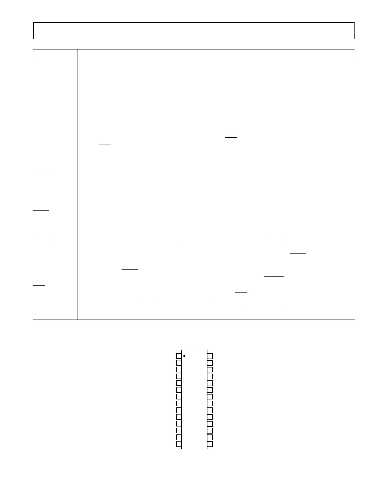
PIN CONFIGURATION
DIP AND SOIC
28
27
26
25
24
23
22
21
20
19
18
17
16
15
AGND
NC
NC
NC
NC
V
DD
V
OUT
V
OUT
CLR
LDAC
FSYNC
PAEN
PA4
PA3
1
3
V
REF
V
REF
V
V
DGND
SCLK
V
DSG
OUT
OUT
V
DIN
PA0
PA1
PA2
SS
(–)
(+)
NC
2
4
CC
1
2
3
4
5
AD7834
6
TOP VIEW
(Not to Scale)
7
8
9
10
11
12
13
14
NC = NO CONNECT
–5–
Loading...