


AD725AR-REEL7
Table of contents
 Loading...
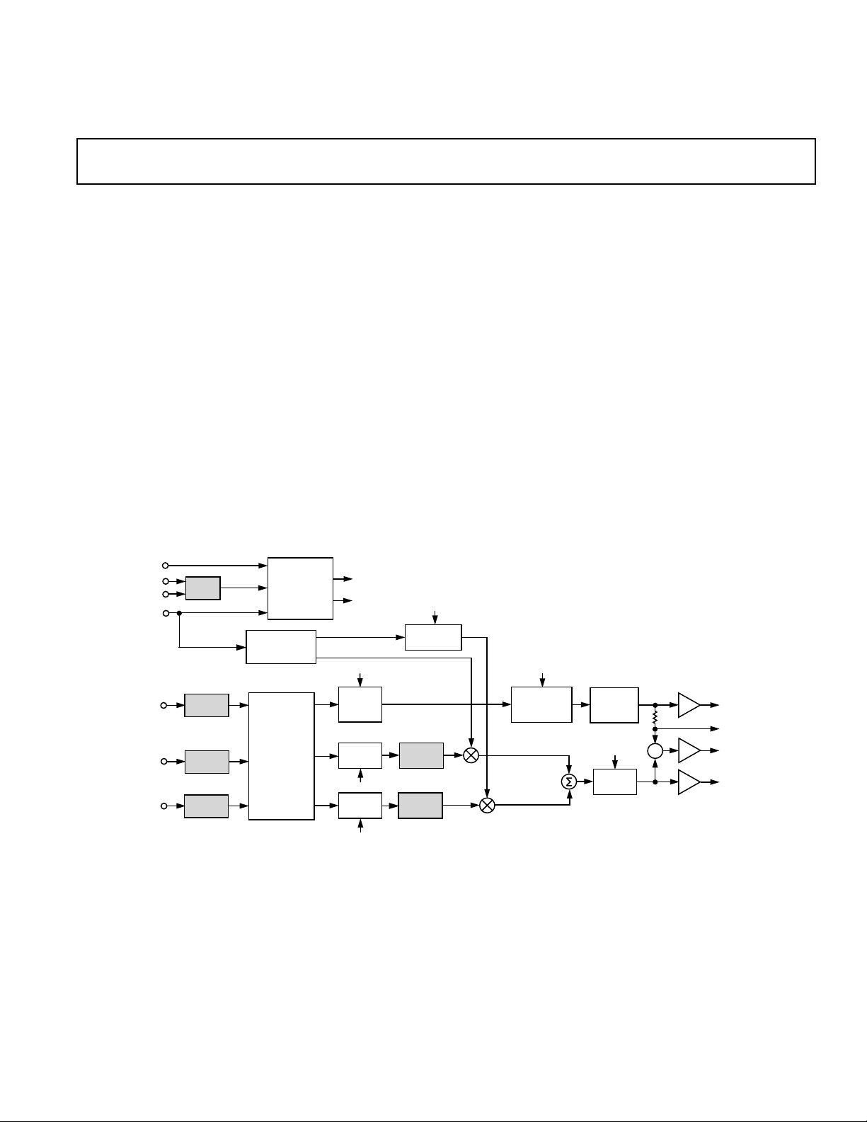
a
Low Cost RGB to NTSC/PAL Encoder
with Luma Trap Port
AD725
One Technology Way, P.O. Box 9106, Norwood, MA 02062-9106, U.S.A.
Tel: 781/329-4700 World Wide Web Site: http://www.analog.com
Fax: 781/326-8703 © Analog Devices, Inc., 1997
FEATURES
Composite Video Output: Both NTSC and PAL
Chrominance and Luminance (S-Video) Outputs
Luma Trap Port to Eliminate Cross Color Artifacts
TTL Logic Levels
Integrated Delay Line and Auto-Tuned Filters
Drives 75 V Reverse-Terminated Loads
Low Power +5 V Operation
Power-Down to <1 mA
Very Low Cost
APPLICATIONS
RGB/VGA to NTSC/PAL Encoding
Personal Computers/Network Computers
Video Games
Video Conference Cameras
Digital Still Cameras
PRODUCT DESCRIPTION
The AD725 is a very low cost general purpose RGB to NTSC/
PAL encoder that converts red, green and blue color compo-
nent signals into their corresponding luminance (baseband
amplitude) and chrominance (subcarrier amplitude and phase)
signals in accordance with either NTSC or PAL standards.
These two outputs are also combined on-chip to provide a
composite video output. All three outputs are available sepa-
rately at voltages of twice the standard signal levels as re-
quired for driving 75 Ω, reverse-terminated cables.
The AD725 features a luminance trap (YTRAP) pin that pro-
vides a means of reducing cross color generated by subcarrier
frequency components found in the luminance signal. For por-
table or other power-sensitive applications, the device can be
powered down to less than 1 µA of current consumption. All
logic levels are TTL compatible thus supporting the logic re-
quirements of 3 V CMOS systems.
The AD725 is packaged in a low cost 16-lead SOIC and oper-
ates from a +5 V supply.
FUNCTIONAL BLOCK DIAGRAM
4FSC
NTSC/PAL
HSYNC
VSYNC
BURST
NTSC/PAL
FSC 90
8
C
FSC 0
8
C
4FSC
FSC 90
8
C/270
8
C
CSYNC
CSYNC
RED
GREEN
BLUE
CSYNC
Y
U
V
BALANCED
MODULATORS
NTSC/PAL
X2
X2
X2
LUMINANCE
OUTPUT
COMPOSITE
OUTPUT
CHROMINANCE
OUTPUT
CLOCK
AT 8FSC
SYNC
SEPARATOR
QUADRATURE
+4
DECODER
BURST
3-POLE
LP PRE-
FILTER
4-POLE
LPF
4-POLE
LPF
6
180
8
C
(PAL ONLY)
RGB-TO-YUV
ENCODING
MATRIX
SAMPLED-
DATA
DELAY LINE
4-POLE
LPF
2-POLE
LP POST-
FILTER
LUMINANCE
TRAP
4FSC CLOCK
V
CLAMP
U
CLAMP
DC
CLAMP
DC
CLAMP
DC
CLAMP
XNOR
S
REV. 0
Information furnished by Analog Devices is believed to be accurate and
reliable. However, no responsibility is assumed by Analog Devices for its
use, nor for any infringements of patents or other rights of third parties
which may result from its use. No license is granted by implication or
otherwise under any patent or patent rights of Analog Devices.

AD725–SPECIFICA TIONS
REV. 0
–2–
(Unless otherwise noted, V
S
= +5, T
A
= +258C, using 4FSC synchronous clock. All loads are
150 V 6 5% at the IC pins. Outputs are measured at the 75 V reverse terminated load.)
Parameter Conditions Min Typ Max Units
SIGNAL INPUTS (RIN, GIN, BIN)
Input Amplitude Full Scale 714 mV p-p
Black Level
1
0.8 V
Input Resistance
2
RIN, GIN, BIN 1 MΩ
Input Capacitance 5pF
LOGIC INPUTS (HSYNC, VSYNC, 4FSC, CE, STND) TTL Logic Levels
Logic Low Input Voltage 1V
Logic High Input Voltage 2V
Logic Low Input Current (DC) 1 µA
Logic High Input Current (DC) 1 µA
VIDEO OUTPUTS
3
Luminance (LUMA)
Bandwidth, –3 dB NTSC 4.4 MHz
PAL 5.2 MHz
Gain Error –7 –2 +7 %
Nonlinearity max p-p 0.3 %
Sync Level NTSC 252 279 310 mV
PAL 264 291 325 mV
DC Black Level 1.3 V
Luminance Trap (YTRAP)
Output Resistance 1.0 kΩ
DC Black Level 1.0 V
Chrominance (CRMA)
Bandwidth, –3 dB NTSC 1.2 MHz
PAL 1.5 MHz
Color Burst Amplitude NTSC 206 255 305 mV p-p
PAL 221 291 362 mV p-p
Color Burst Width NTSC 2.51 µs
PAL 2.28 µs
Chroma Level Error
4
–4 %
Chroma Phase Error
5
±3 Degrees
DC Black Level 2.0 V
Chroma Feedthrough R, G, B = 0 15 40 mV p-p
Composite (COMP)
Absolute Gain Error With Respect to Luma –5 –1 +3 %
Differential Gain With Respect to Chroma 0.5 %
Differential Phase With Respect to Chroma 1.5 Degrees
DC Black Level 1.4 V
Chroma/Luma Time Alignment S-Video 20 ns
POWER SUPPLIES
Recommended Supply Range Single Supply +4.75 +5.25 V
Quiescent Current—Encode Mode 30 36 mA
Quiescent Current—Power Down <1 µA
NOTES
1
R, G, and B signals are inputted via an external ac coupling capacitor.
2
Except during dc restore period (back porch clamp).
3
All outputs measured at a 75 Ω reverse-terminated load; ac voltages at the IC output pins are twice those specified here.
4
Difference between ideal and actual color bar subcarrier amplitudes.
5
Difference between ideal and actual color bar subcarrier phases.
Specifications are subject to change without notice.
AD725
REV. 0
–3–
ORDERING GUIDE
Temperature Package Package
Model Range Description Option
AD725AR –40°C to +85°C 16-Lead SOIC R-16
AD725AR-Reel –40°C to +85°C 16-Lead SOIC R-16
AD725AR-Reel7 –40°C to +85°C 16-Lead SOIC R-16
AD725-EB Evaluation Board
ABSOLUTE MAXIMUM RATINGS*
Supply Voltage, APOS to AGND . . . . . . . . . . . . . . . . . . +6 V
Supply Voltage, DPOS to DGND . . . . . . . . . . . . . . . . . . +6 V
AGND to DGND . . . . . . . . . . . . . . . . . . . . . –0.3 V to +0.3 V
Inputs . . . . . . . . . . . . . . . . . . . DGND – 0.3 to DPOS + 0.3 V
Internal Power Dissipation . . . . . . . . . . . . . . . . . . . . . .800 mW
Operating Temperature Range . . . . . . . . . . . .–40°C to +85°C
Storage Temperature Range . . . . . . . . . . . . .–65°C to +125°C
Lead Temperature Range (Soldering 30sec) . . . . . . . . +230°C
*Stresses above those listed under Absolute Maximum Ratings may cause perma-
nent damage to the device. This is a stress rating only; functional operation of the
device at these or any other conditions above those indicated in the operational
section of this specification is not implied. Exposure to absolute maximum rating
conditions for extended periods may affect device reliability.
Thermal Characteristics: 16-Pin SOIC Package: θ
JA
= 100°C/W.
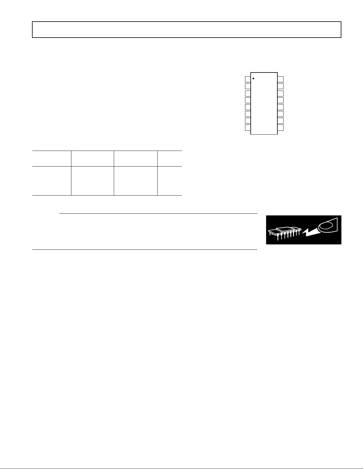
PIN CONFIGURATION
16-Lead Wide Body (SOIC)
(R-16)
AGND
CE
RIN
GIN
4FSC
APOS
BIN
STND
HSYNC
VSYNC
YTRAP
LUMA
COMP
DPOS
DGND
CRMA
1
2
16
15
5
6
7
12
11
10
3
4
14
13
89
TOP VIEW
(Not to Scale)
AD725
CAUTION
ESD (electrostatic discharge) sensitive device. Electrostatic charges as high as 4000 V readily
accumulate on the human body and test equipment and can discharge without detection.
Although the AD725 features proprietary ESD protection circuitry, permanent damage may
occur on devices subjected to high energy electrostatic discharges. Therefore, proper ESD
precautions are recommended to avoid performance degradation or loss of functionality.
WARNING!
ESD SENSITIVE DEVICE
REV. 0
–4–
AD725
PIN DESCRIPTIONS
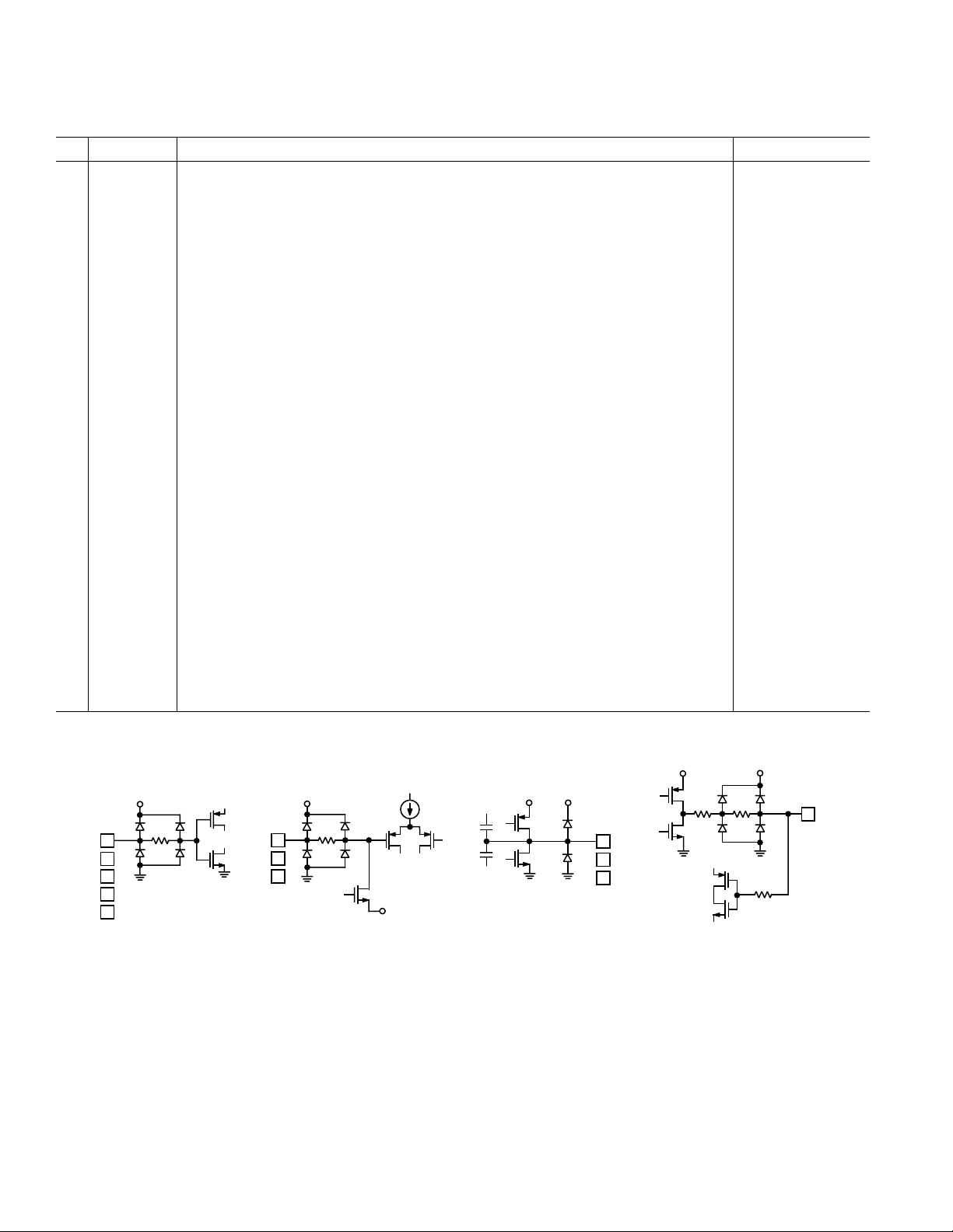
Pin Mnemonic Description Equivalent Circuit
1 STND Encoding Standard Pin. A Logic HIGH input selects NTSC encoding. Circuit A
A Logic LOW input selects PAL encoding.
TTL Logic Levels.
2 AGND Analog Ground Connection.
3 4FSC 4FSC Clock Input. Circuit A
For NTSC: 14.318 180 MHz.
For PAL: 17.734 475 MHz.
TTL Logic Levels.
4 APOS Analog Positive Supply (+5 V ± 5%).
5 CE Chip Enable. A Logic HIGH input enables the encode function. Circuit A
A Logic LOW input powers down chip when not in use.
TTL Logic Levels.
6 RIN Red Component Video Input. Circuit B
0 mV to 714 mV AC-Coupled.
7 GIN Green Component Video Input. Circuit B
0 mV to 714 mV AC-Coupled.
8 BIN Blue Component Video Input. Circuit B
0 mV to 714 mV AC-Coupled.
9 CRMA Chrominance Output.* Circuit C
Approximately 1.8 V peak-to-peak for both NTSC and PAL.
10 COMP Composite Video Output.* Circuit C
Approximately 2.5 V peak-to-peak for both NTSC and PAL.
11 LUMA Luminance plus CSYNC Output.* Circuit C
Approximately 2 V peak-to-peak for both NTSC and PAL.
12 YTRAP Luminance Trap Filter Tap. Attach L-C resonant network to reduce cross-color artifacts. Circuit D
13 DGND Digital Ground Connection.
14 DPOS Digital Positive Supply (+5 V ± 5%).
15 VSYNC Vertical Sync Signal (if using external CSYNC set at > +2 V). TTL Logic Levels. Circuit A
16 HSYNC Horizontal Sync Signal (or CSYNC signal). TTL Logic Levels. Circuit A
*The Luminance, Chrominance and Composite Outputs are at twice normal levels for driving 75 Ω reverse-terminated lines.
7
V
CLAMP
6
8
DPOS
DGND
3
1
5
15
16
DPOS
DGND
10
9
11
APOS
AGND
DGND
DPOS
APOS
AGND
DGND
DPOS
12
1kV
Circuit A Circuit B Circuit C Circuit D
Figure 1. Equivalent Circuits
REV. 0
–5–
T ypical Characteristics–AD725
IRE
µs
1.0
0.5
–0.5
06010 20 30 40 50
0.0
APL = 50.8%
525 LINE NTSC NO FILTERING
SLOW CLAMP TO 0.00V @ 6.63
m
s
100
50
0
–50
VOLTS
Figure 3. 100% Color Bars, NTSC
Figure 4. 100% Color Bars on Vector Scope, NTSC
RGB
3
75V
75V
COMPOSITE
VIDEO
COMPOSITE
SYNC
FSC
GENLOCK
TEKTRONIX
TG2000
SIGNAL
GENERATION
PLATFORM
AD725
RGB TO
NTSC/PAL
ENCODER
TEKTRONIX
VM700A
WAVEFORM
MONITOR
SONY
MONITOR
MODEL
PVM-1354Q
+5V
4FSC
HP3314A
3 4 PLL
FSC
(3.579545MHz
OR
4.433618MHz)
OSCILLATOR
Figure 2. Evaluation Setup
ms
1.0
0.5
–0.5
06010 20 30 40 50
0.0
VOLTS
APL = 50.6%
625 LINE PAL NO FILTERING
SLOW CLAMP TO 0.00V @ 6.72
m
s
Figure 5. 100% Color Bars, PAL
Figure 6. 100% Color Bars on Vector Scope, PAL
REV. 0
–6–
AD725–Typical Characteristics
APL = 46.6%
525 LINE NTSC NO FILTERING
SLOW CLAMP TO 0.00V
@ 6.63ms
ms
06010 20 30 40 50
IRE
1.0
0.5
–0.5
0.0
100
50
0
–50
VOLTS
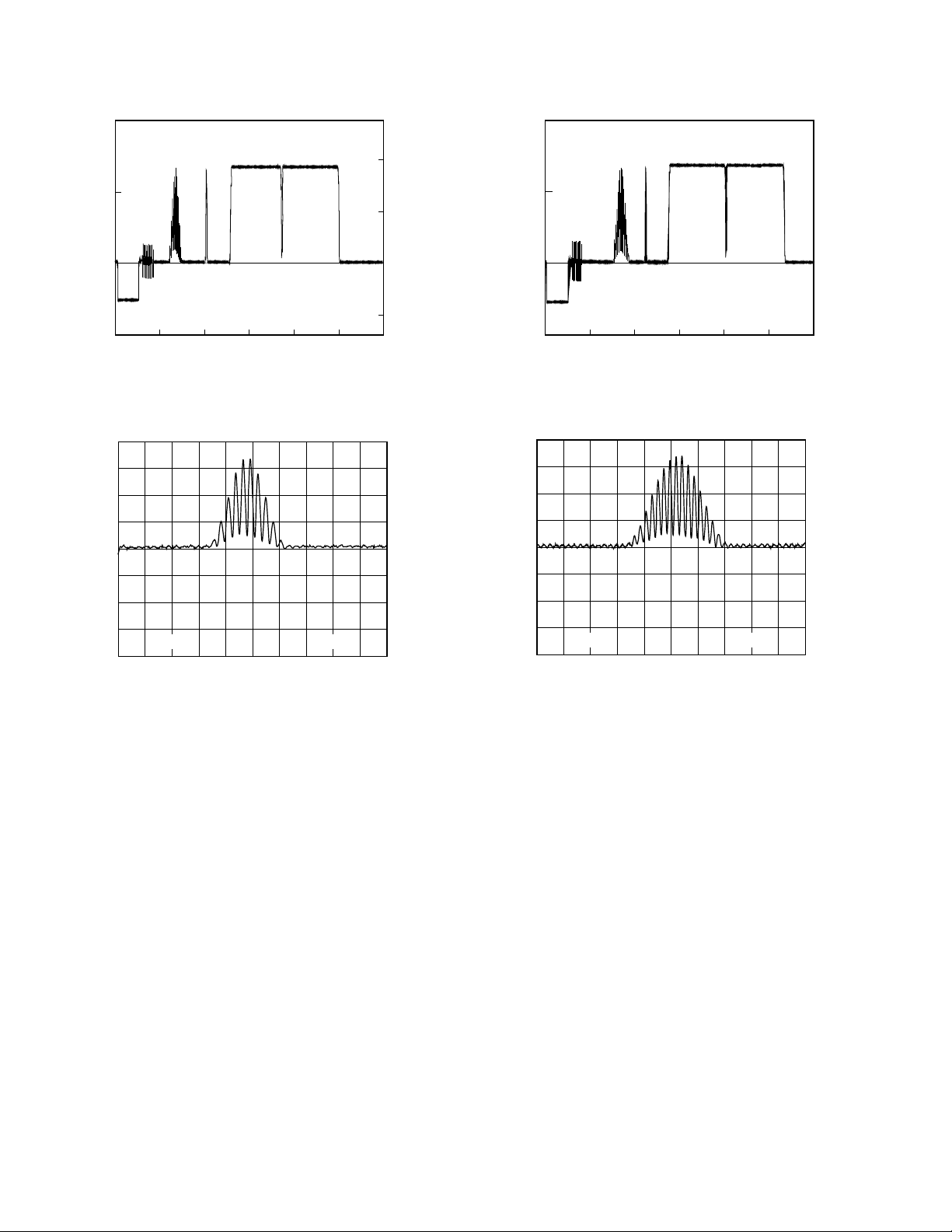
Figure 7. Modulated Pulse and Bar, NTSC
200mV 1
m
s
Figure 8. Zoom on Modulated Pulse, NTSC
ms
1.0
0.5
–0.5
06010 20 30 40 50
0.0
APL = 33.5%
625 LINE PAL NO FILTERING
SLOW CLAMP TO 0.00V
@ 6.72 ms
VOLTS
Figure 9. Modulated Pulse and Bar, PAL
200mV 1
m
s
Figure 10. Zoom on Modulated Pulse, PAL
Loading...