


 Loading...
Analog Devices AD7528UQ, AD7528TQ, AD7528SQ, AD7528LP, AD7528LN Datasheet
...
a |
CMOS Dual 8-Bit |
|
Buffered Multiplying DAC |
||
|
|
|
|
|
AD7528 |
|
|
|
FEATURES
On-Chip Latches for Both DACs +5 V to +15 V Operation
DACs Matched to 1%
Four Quadrant Multiplication TTL/CMOS Compatible
Latch Free (Protection Schottkys not Required)
APPLICATIONS
Digital Control of:
Gain/Attenuation
Filter Parameters
Stereo Audio Circuits
X-Y Graphics
FUNCTIONAL BLOCK DIAGRAM
|
|
|
VREF A |
|
V |
|
|
RFB A |
|
DD |
|
|
|
|
DB0 |
|
|
OUT A |
|
DATA |
INPUT |
|
||
LATCH |
DAC A |
|||
INPUTS |
BUFFER |
|||
|
|
|||
|
|
|
AGND |
|
DAC A/ |
|
|
AD7528 |
|
DAC B |
|
|
RFB B |
|
CS |
CONTROL |
|
||
|
|
|||
LOGIC |
|
|
||
WR |
|
OUT B |
||
|
LATCH |
|||
|
|
DAC B |
||
DGND |
|
|
|
|
|
|
|
VREF B |
GENERAL DESCRIPTION
The AD7528 is a monolithic dual 8-bit digital/analog converter featuring excellent DAC-to-DAC matching. It is available in skinny 0.3" wide 20-lead DIPs and in 20-lead surface mount packages.
Separate on-chip latches are provided for each DAC to allow easy microprocessor interface.
Data is transferred into either of the two DAC data latches via a common 8-bit TTL/CMOS compatible input port. Control input DAC A/DAC B determines which DAC is to be loaded. The AD7528’s load cycle is similar to the write cycle of a random access memory and the device is bus compatible with most 8-bit microprocessors, including 6800, 8080, 8085, Z80.
The device operates from a +5 V to +15 V power supply, dissipating only 20 mW of power.
Both DACs offer excellent four quadrant multiplication characteristics with a separate reference input and feedback resistor for each DAC.
PRODUCT HIGHLIGHTS
1.DAC-to-DAC matching: since both of the AD7528 DACs are fabricated at the same time on the same chip, precise matching and tracking between DAC A and DAC B is inherent.
The AD7528’s matched CMOS DACs make a whole new range of applications circuits possible, particularly in the audio, graphics and process control areas.
2.Small package size: combining the inputs to the on-chip DAC latches into a common data bus and adding a DAC A/DAC B select line has allowed the AD7528 to be packaged in either a small 20-lead DIP, SOIC or PLCC.
REV. B
Information furnished by Analog Devices is believed to be accurate and reliable. However, no responsibility is assumed by Analog Devices for its use, nor for any infringements of patents or other rights of third parties which may result from its use. No license is granted by implication or otherwise under any patent or patent rights of Analog Devices.
ORDERING GUIDE1
|
Temperature |
Relative |
Gain |
Package |
Model2 |
Ranges |
Accuracy |
Error |
Options3 |
AD7528JN |
–40°C to +85°C |
±1 LSB |
±4 LSB |
N-20 |
AD7528KN |
–40°C to +85°C |
±1/2 LSB |
±2 LSB |
N-20 |
AD7528LN |
–40°C to +85°C |
±1/2 LSB |
±1 LSB |
N-20 |
AD7528JP |
–40°C to +85°C |
±1 LSB |
±4 LSB |
P-20A |
AD7528KP |
–40°C to +85°C |
±1/2 LSB |
±2 LSB |
P-20A |
AD7528LP |
–40°C to +85°C |
±1/2 LSB |
±1 LSB |
P-20A |
AD7528JR |
–40°C to +85°C |
±1 LSB |
±4 LSB |
R-20 |
AD7528KR |
–40°C to +85°C |
±1/2 LSB |
±2 LSB |
R-20 |
AD7528LR |
–40°C to +85°C |
±1/2 LSB |
±1 LSB |
R-20 |
AD7528AQ |
–40°C to +85°C |
±1 LSB |
±4 LSB |
Q-20 |
AD7528BQ |
–40°C to +85°C |
±1/2 LSB |
±2 LSB |
Q-20 |
AD7528CQ |
–40°C to +85°C |
±1/2 LSB |
±1 LSB |
Q-20 |
AD7528SQ |
–55°C to +125°C |
±1 LSB |
±4 LSB |
Q-20 |
AD7528TQ |
–55°C to +125°C |
±1/2 LSB |
±2 LSB |
Q-20 |
AD7528UQ |
–55°C to +125°C |
±1/2 LSB |
±1 LSB |
Q-20 |
NOTES
1Analog Devices reserves the right to ship side-brazed ceramic in lieu of cerdip. Parts will be marked with cerdip designator “Q.”
2Processing to MIL-STD-883C, Class B is available. To order, add suffix “/883B” to part number. For further information, see Analog Devices’ 1990 Military Products Databook.
3N = Plastic DIP; P = Plastic Leaded Chip Carrier; Q = Cerdip; R = SOIC.
One Technology Way, P.O. Box 9106, Norwood, MA 02062-9106, U.S.A.
Tel: 781/329-4700 |
World Wide Web Site: http://www.analog.com |
Fax: 781/326-8703 |
© Analog Devices, Inc., 1998 |
AD7528–SPECIFICATIONS (VREF A = VREF B = +10 V; OUT A = OUT B = O V unless otherwise noted)
|
|
|
|
VDD = +5 V |
VDD = +15 V |
|
|
||
Parameter |
Version1 |
TA = +25°C |
TMIN, TMAX |
TA= +25°C |
TMIN, TMAX |
Units |
Test Conditions/Comments |
||
STATIC PERFORMANCE2 |
|
|
|
|
|
|
|
||
Resolution |
All |
8 |
8 |
8 |
8 |
Bits |
|
||
Relative Accuracy |
J, A, S |
± 1 |
± 1 |
± 1 |
± 1 |
LSB max |
This is an Endpoint Linearity Specification |
||
|
|
|
K, B, T |
± 1/2 |
± 1/2 |
± 1/2 |
± 1/2 |
LSB max |
|
|
|
|
L, C, U |
± 1/2 |
± 1/2 |
± 1/2 |
± 1/2 |
LSB max |
|
Differential Nonlinearity |
All |
± 1 |
± 1 |
± 1 |
± 1 |
LSB max |
All Grades Guaranteed Monotonic Over |
||
|
|
|
|
± 4 |
± 6 |
± 4 |
± 5 |
|
Full Operating Temperature Range |
Gain Error |
J, A, S |
LSB max |
Measured Using Internal RFB A and RFB B |
||||||
|
|
|
K, B, T |
± 2 |
± 4 |
± 2 |
± 3 |
LSB max |
Both DAC Latches Loaded with 11111111 |
|
|
|
L, C, U |
± 1 |
± 3 |
± 1 |
± 1 |
LSB max |
Gain Error is Adjustable Using Circuits |
Gain Temperature Coefficient3 |
|
|
|
|
|
|
of Figures 4 and 5 |
||
|
± 0.007 |
± 0.007 |
± 0.0035 |
± 0.0035 |
%/°C max |
|
|||
Gain/ Temperature |
All |
|
|||||||
Output Leakage Current |
|
± 50 |
± 400 |
± 50 |
± 200 |
|
|
||
OUT A (Pin 2) |
All |
nA max |
DAC Latches Loaded with 00000000 |
||||||
OUT B (Pin 20) |
All |
± 50 |
± 400 |
± 50 |
± 200 |
nA max |
|
||
Input Resistance (VREF A, VREF B) |
All |
8 |
8 |
8 |
8 |
kΩ min |
Input Resistance TC = –300 ppm/°C, Typical |
||
VREF A/VREF B Input Resistance |
|
15 |
15 |
15 |
15 |
kΩ max |
Input Resistance is 11 kΩ |
||
|
± 1 |
± 1 |
± 1 |
± 1 |
|
|
|||
Match |
All |
% max |
|
||||||
|
|
|
|
|
|
|
|
|
|
DIGITAL INPUTS4 |
|
|
|
|
|
|
|
||
Input High Voltage |
|
|
|
|
|
|
|
||
VIH |
All |
2.4 |
2.4 |
13.5 |
13.5 |
V min |
|
||
Input Low Voltage |
|
|
|
|
|
|
|
||
VIL |
All |
0.8 |
0.8 |
1.5 |
1.5 |
V max |
|
||
Input Current |
|
± 1 |
± 10 |
± 1 |
± 10 |
µA max |
|
||
IIN |
All |
VIN = 0 or VDD |
|||||||
Input Capacitance |
|
|
|
|
|
|
|
||
DB0–DB7 |
All |
10 |
10 |
10 |
10 |
pF max |
|
||
WR, CS, |
DAC A |
/DAC B |
All |
15 |
15 |
15 |
15 |
pF max |
|
|
|
|
|
|
|
|
|
|
|
SWITCHING CHARACTERISTICS3 |
|
|
|
|
|
|
See Timing Diagram |
||
Chip Select to Write Set Up Time |
|
|
|
|
|
|
|
||
tCS |
All |
90 |
100 |
60 |
80 |
ns min |
|
||
Chip Select to Write Hold Time |
|
|
|
|
|
|
|
||
tCH |
All |
0 |
0 |
10 |
15 |
ns min |
|
||
DAC Select to Write Set Up Time |
|
|
|
|
|
|
|
||
tAS |
All |
90 |
100 |
60 |
80 |
ns min |
|
||
DAC Select to Write Hold Time |
|
|
|
|
|
|
|
||
tAH |
All |
0 |
0 |
10 |
15 |
ns min |
|
||
Data Valid to Write Set Up Time |
|
|
|
|
|
|
|
||
tDS |
All |
80 |
90 |
30 |
40 |
ns min |
|
||
Data Valid to Write Hold Time |
|
|
|
|
|
|
|
||
tDH |
All |
0 |
0 |
0 |
0 |
ns min |
|
||
Write Pulsewidth |
|
|
|
|
|
|
|
||
tWR |
All |
90 |
100 |
60 |
80 |
ns min |
|
||
POWER SUPPLY |
|
|
|
|
|
|
See Figure 3 |
||
IDD |
All |
2 |
2 |
2 |
2 |
mA max |
All Digital Inputs VIL or VIH |
||
|
|
|
All |
100 |
500 |
100 |
500 |
µA max |
All Digital Inputs 0 V or VDD |
|
|
|
5 |
(Measured Using Recommended P.C. Board Layout (Figure 7) and AD644 as |
||||||
AC PERFORMANCE CHARACTERISTICS |
Output Amplifiers) |
|
|
|
|
|||||
|
|
VDD = +5 V |
|
VDD = +15 V |
|
|
|
|
||
Parameter |
Version1 |
TA = +25°C |
TMIN, TMAX |
TA= +25°C |
TMIN, TMAX |
Units |
Test Conditions/Comments |
|||
DC SUPPLY REJECTION ( GAIN/ VDD) |
All |
0.02 |
0.04 |
|
0.01 |
0.02 |
% per % max |
VDD = ± 5% |
||
|
|
|
|
|
|
|
|
|
|
|
CURRENT SETTLING TIME2 |
All |
350 |
400 |
|
180 |
200 |
ns max |
To 1/2 LSB. OUT A/OUT B Load = 100 Ω. |
||
|
|
|
|
|
|
|
|
WR = |
CS |
= 0 V. DB0–DB7 = 0 V to VDD or |
|
|
|
|
|
|
|
|
VDD to 0 V |
||
PROPAGATION DELAY (From Digital In- |
|
|
|
|
|
|
|
VREF A = VREF B = +10 V |
||
put to 90% of Final Analog Output Current) |
All |
220 |
270 |
|
80 |
100 |
ns max |
OUT A, OUT B Load = 100 Ω CEXT = 13 pF |
||
|
|
|
|
|
|
|
|
WR = CS = 0 V DB0–DB7 = 0 V to VDD or |
||
|
|
|
|
|
|
|
|
VDD to 0 V |
||
DIGITAL-TO-ANALOG GLITCH IMPULSE |
All |
160 |
|
|
440 |
|
nV sec typ |
For Code Transition 00000000 to 11111111 |
||
|
|
|
|
|
|
|
|
|
|
|
OUTPUT CAPACITANCE |
|
|
|
|
|
|
|
|
|
|
COUTA |
All |
50 |
50 |
|
50 |
50 |
pF max |
DAC Latches Loaded with 00000000 |
||
COUTB |
|
50 |
50 |
|
50 |
50 |
pF max |
|
|
|
COUTA |
|
120 |
120 |
|
120 |
120 |
pF max |
DAC Latches Loaded with 11111111 |
||
COUTB |
|
120 |
120 |
|
120 |
120 |
pF max |
|
|
|
AC FEEDTHROUGH6 |
|
|
|
|
|
|
|
|
|
|
VREF A to OUT A |
All |
–70 |
–65 |
|
–70 |
–65 |
dB max |
VREF A, VREF B = 20 V p-p Sine Wave |
||
VREF B to OUT B |
|
–70 |
–65 |
|
–70 |
–65 |
dB max |
@ 100 kHz |
||
–2– |
REV. B |
|
|
|
|
|
|
|
AD7528 |
|
|
|
|
|
|
|
|
|
|
VDD = +5 V |
VDD = +15 V |
|
|
||
Parameter |
Version1 |
TA = +25°C |
TMIN, TMAX |
TA= +25°C |
TMIN, TMAX |
Units |
Test Conditions/Comments |
CHANNEL-TO-CHANNEL ISOLATION |
|
|
|
|
|
|
Both DAC Latches Loaded with 11111111. |
VREF A to OUT B |
All |
–77 |
|
–77 |
|
dB typ |
VREF A = 20 V p-p Sine Wave @ 100 kHz |
|
|
|
|
|
|
|
VREF B = 0 V see Figure 6. |
VREF B to OUT A |
|
–77 |
|
–77 |
|
dB typ |
VREF A = 20 V p-p Sine Wave @ 100 kHz |
|
|
|
|
|
|
|
VREF A = 0 V see Figure 6. |
DIGITAL CROSSTALK |
All |
30 |
|
60 |
|
nV sec typ |
Measured for Code Transition 00000000 to |
|
|
|
|
|
|
|
11111111 |
|
|
|
|
|
|
|
|
HARMONIC DISTORTlON |
All |
–85 |
|
–85 |
|
dB typ |
VIN = 6 V rms @ 1 kHz |
|
|
|
|
|
|
|
|
NOTES
1Temperature Ranges are J, K, L Versions: –40°C to +85°C A, B, C Versions: –40°C to +85°C S, T, U Versions: –55°C to +125°C
2Specifications applies to both DACs in AD7528.
3Guaranteed by design but not production tested.
4Logic inputs are MOS Gates. Typical input current (+25°C) is less than 1 nA. 5These characteristics are for design guidance only and are not subject to test.
6Feedthrough can be further reduced by connecting the metal lid on the ceramic package (suffix D) to DGND.
AD7528, ideal maximum output is VREF – 1 LSB. Gain error of both DACs is adjustable to zero with external resistance.
Output Capacitance
Capacitance from OUT A or OUT B to AGND.
Digital to Analog Glitch lmpulse
Specifications subject to change without notice.
ABSOLUTE MAXIMUM RATINGS
(TA = +25°C unless otherwise noted)
VDD to AGND . . . . . . . . . . . . . . . . . . . . . |
. . |
. . . . . 0 V, +17 V |
VDD to DGND . . . . . . . . . . . . . . . . . . . . . . |
. . |
. . . . 0 V, +17 V |
AGND to DGND . . . . . . . . . . . . . . . . . . . |
. . |
. . . VDD + 0.3 V |
DGND to AGND . . . . . . . . . . . . . . . . . . . |
. . |
. . . VDD + 0.3 V |
Digital Input Voltage to DGND . . . . . . . |
–0.3 V, VDD + 0.3 V |
|
VPIN2, VPIN20 to AGND . . . . . . . . . . . . . . |
–0.3 V, VDD + 0.3 V |
|
VREF A, VREF B to AGND . . . . . . . . . . . . . |
. . |
. . . . . . . . ±25 V |
VRFB A, VRFB B to AGND . . . . . . . . . . . . . |
. . |
. . . . . . . . ±25 V |
Power Dissipation (Any Package) to +75°C . |
. . . . . . 450 mW |
|
Derates above +75°C by . . . . . . . . . . . . |
. . |
. . . . . 6 mW/°C |
Operating Temperature Range |
|
–40°C to +85°C |
Commercial (J, K, L) Grades . . . . . . . . . |
. . |
|
Industrial (A, B, C) Grades . . . . . . . . . . |
. . |
–40°C to +85°C |
Extended (S, T, U) Grades . . . . . . . . . . |
. |
–55°C to +125°C |
Storage Temperature . . . . . . . . . . . . . . . . . |
. |
–65°C to +150°C |
Lead Temperature (Soldering, 10 secs) . . . |
. . |
. . . . . . .+300°C |
CAUTION:
1.ESD sensitive device. The digital control inputs are diode protected; however, permanent damage may occur on unconnected devices subjected to high energy electrostatic fields. Unused devices must be stored in conductive foam or shunts.
The amount of charge injected from the digital inputs to the analog output when the inputs change state. This is normally specified as the area of the glitch in either pA-secs or nV-secs depending upon whether the glitch is measured as a current or voltage signal. Glitch impulse is measured with VREF A,
VREF B = AGND.
Propagation Delay
This is a measure of the internal delays of the circuit and is defined as the time from a digital input change to the analog output current reaching 90% of its final value.
Channel-to-Channel Isolation
The proportion of input signal from one DAC’s reference input which appears at the output of the other DAC, expressed as a ratio in dB.
Digital Crosstalk
The glitch energy transferred to the output of one converter due to a change in digital input code to the other converter. Specified in nV secs.
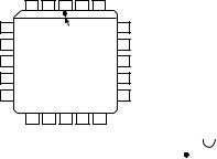
PIN CONFIGURATIONS
PLCC
R |
OUTA |
AGND |
OUTB |
R |
A |
|
|
|
B |
FB |
|
|
|
FB |
3 |
2 |
1 |
20 |
19 |
2.Do not insert this device into powered sockets. Remove power before insertion or removal.
TERMINOLOGY
Relative Accuracy
Relative accuracy or endpoint nonlinearity is a measure of the maximum deviation from a straight line passing through the endpoints of the DAC transfer function. It is measured after adjusting for zero and full scale and is normally expressed in LSBs or as a percentage of full scale reading.
Differential Nonlinearity
Differential nonlinearity is the difference between the measured change and the ideal 1 LSB change between any two adjacent codes. A specified differential nonlinearity of ±1 LSB max over the operating temperature range ensures monotonicity.
Gain Error
Gain error or full-scale error is a measure of the output error between an ideal DAC and the actual device output. For the
VREF A |
4 |
|
|
|
|
|
PIN 1 |
|
18 |
VREF B |
|
|
|
|
|
|
||
|
|
|
|
|
|
|
IDENTIFIER |
|
|
|
|
|
|
|
||||
DGND |
5 |
|
|
AD7528 |
|
17 |
VDD |
|
|
|
|
|
|
|||||
DAC A/DAC B |
6 |
|
|
|
16 |
WR |
|
|
|
|
|
|
||||||
|
|
TOP VIEW |
|
|
|
|
|
|
|
|||||||||
|
|
|
|
|
|
|
|
|
|
|
|
|
||||||
(MSB) DB7 |
7 |
|
(Not to Scale) |
15 |
CS |
|
|
|
|
|
|
|||||||
DB6 |
8 |
|
|
|
|
|
|
|
|
|
14 |
DB0 (LSB) |
|
|
|
|
|
|
|
|
|
|
|
|
|
|
|
|
|
|
|
|
|
|
|
|
|
|
|
9 |
|
10 |
|
11 |
|
12 |
|
13 |
|
|
DIP, SOIC |
|
|
|||
|
|
DB5 |
|
DB4 |
DB3 |
|
DB2 |
DB1 |
|
AGND |
|
OUT B |
||||||
|
|
|
|
|
|
|
|
|
|
|||||||||
|
|
|
|
|
|
|
|
|
|
|
|
1 |
|
|
|
20 |
||
|
|
|
|
|
|
|
|
|
|
|
|
OUT A |
|
|
|
|
|
RFB B |
|
|
|
|
|
|
|
|
|
|
|
|
2 |
|
|
|
19 |
||
|
|
|
|
|
|
|
|
|
|
|
|
RFB A |
|
|
|
|
|
VREF B |
|
|
|
|
|
|
|
|
|
|
|
|
3 |
|
|
|
18 |
||
|
|
|
|
|
|
|
|
|
|
|
|
VREF A |
|
|
|
|
|
VDD |
|
|
|
|
|
|
|
|
|
|
|
|
4 |
|
|
|
17 |
||
|
|
|
|
|
|
|
|
|
|
|
|
|
|
AD7528 |
|
|
||
|
|
|
|
|
|
|
|
|
|
|
|
DGND |
5 |
16 |
WR |
|||
|
|
|
|
|
|
|
|
|
|
|
|
|
|
TOP VIEW |
|
|
||
|
|
|
|
|
|
|
|
|
|
|
DAC A/DAC B |
6 |
15 |
CS |
||||
|
|
|
|
|
|
|
|
|
|
|
(Not to Scale) |
|||||||
|
|
|
|
|
|
|
|
|
|
|
(MSB) DB7 |
|
|
DB0 (LSB) |
||||
|
|
|
|
|
|
|
|
|
|
|
7 |
|
|
|
14 |
|||
|
|
|
|
|
|
|
|
|
|
|
|
DB6 |
|
|
|
|
|
DB1 |
|
|
|
|
|
|
|
|
|
|
|
|
8 |
|
|
|
13 |
||
|
|
|
|
|
|
|
|
|
|
|
|
DB5 |
|
|
|
|
|
DB2 |
|
|
|
|
|
|
|
|
|
|
|
|
9 |
|
|
|
12 |
||
|
|
|
|
|
|
|
|
|
|
|
|
DB4 |
|
|
|
|
|
|
|
|
|
|
|
|
|
|
|
|
|
|
10 |
|
|
|
11 |
DB3 |
|
|
|
|
|
|
|
|
|
|
|
|
|
|
|
|
|
|
|
|
REV. B |
–3– |
Loading...