


Analog Devices AD8001AR, AD8001AQ, AD8001AN, AD8001ACHIPS, AD8001R-EB Datasheet
...a |
800 MHz, 50 mW |
|
Current Feedback Amplifier |
||
|
|
AD8001 |
|
|
|
FEATURES
Excellent Video Specifications (RL = 150 V, G = +2)
Gain Flatness 0.1 dB to 100 MHz 0.01% Differential Gain Error 0.0258 Differential Phase Error
Low Power
5.5 mA Max Power Supply Current (55 mW) High Speed and Fast Settling
880 MHz, –3 dB Bandwidth (G = +1)
440 MHz, –3 dB Bandwidth (G = +2)
1200 V/ms Slew Rate
10 ns Settling Time to 0.1% Low Distortion
–65 dBc THD, fC = 5 MHz
33 dBm 3rd Order Intercept, F1 = 10 MHz –66 dB SFDR, f = 5 MHz
High Output Drive
70 mA Output Current
Drives Up to Four Back-Terminated Loads (75 V Each)
While Maintaining Good Differential Gain/Phase Performance (0.05%/0.258)
APPLICATIONS
A-to-D Driver
Video Line Driver
Professional Cameras
Video Switchers
Special Effects
RF Receivers
PRODUCT DESCRIPTION
The AD8001 is a low power, high-speed amplifier designed to operate on ±5 V supplies. The AD8001 features unique
|
9 |
|
|
|
|
|
VS = 65V |
|
6 |
|
RFB = 820V |
|
3 |
G = +2 |
|
|
RL = 100V |
|
|
|
|
|
|
dB |
0 |
|
|
– |
|
|
|
–3 |
|
|
|
GAIN |
VS = 65V |
|
|
|
|
|
|
|
|
RFB = 1kV |
|
|
–6 |
|
|
|
–9 |
|
|
|
–12 |
|
|
|
10M |
100M |
1G |
|
|
FREQUENCY – Hz |
|
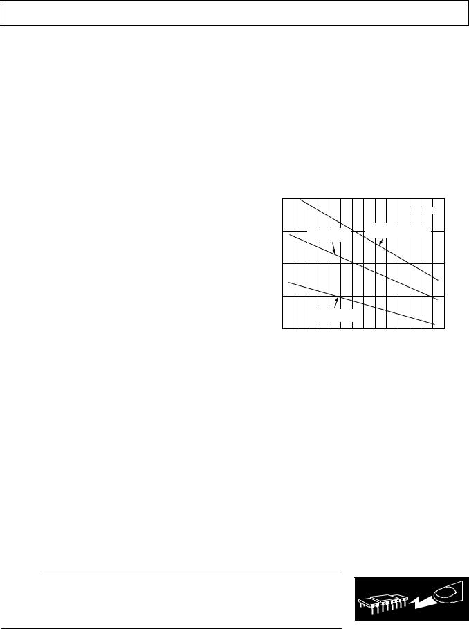
Figure 1. Frequency Response of AD8001
FUNCTIONAL BLOCK DIAGRAMS
8-Lead DIP (N-8, Q-8) |
5-Lead |
and SOIC (SO-8) |
SOT-23-5 |
NC |
1 |
|
8 |
NC |
–IN 2 |
|
7 |
V+ |
|
+IN |
3 |
|
6 |
OUT |
V– 4 |
AD8001 |
5 |
NC |
|
|
|
|
|
|
NC = NO CONNECT
|
|
AD8001 |
|
VOUT |
1 |
5 |
+VS |
–V |
2 |
|
|
S |
|
|
|
+IN |
3 |
4 |
–IN |
transimpedance linearization circuitry. This allows it to drive video loads with excellent differential gain and phase performance on only 50 mW of power. The AD8001 is a current feedback amplifier and features gain flatness of 0.1 dB to 100 MHz while offering differential gain and phase error of 0.01% and 0.025°. This makes the AD8001 ideal for professional video electronics such as cameras and video switchers. Additionally, the AD8001’s low distortion and fast settling make it ideal for buffer high-speed A-to-D converters.
The AD8001 offers low power of 5.5 mA max (VS = ±5 V) and can run on a single +12 V power supply, while being capable of delivering over 70 mA of load current. These features make this amplifier ideal for portable and battery-powered applications where size and power are critical.
The outstanding bandwidth of 800 MHz along with 1200 V/ s of slew rate make the AD8001 useful in many general purpose high-speed applications where dual power supplies of up to ±6 V and single supplies from 6 V to 12 V are needed. The AD8001 is available in the industrial temperature range of –40°C to +85°C.
Figure 2. Transient Response of AD8001; 2 V Step, G = +2
REV. C
Information furnished by Analog Devices is believed to be accurate and reliable. However, no responsibility is assumed by Analog Devices for its use, nor for any infringements of patents or other rights of third parties which may result from its use. No license is granted by implication or otherwise under any patent or patent rights of Analog Devices.
One Technology Way, P.O. Box 9106, Norwood, MA 02062-9106, U.S.A.
Tel: 781/329-4700 |
World Wide Web Site: http://www.analog.com |
Fax: 781/326-8703 |
© Analog Devices, Inc., 1999 |
AD8001–SPECIFICATIONS (@ TA = + 258C, VS = 65 V, RL = 100 V, unless otherwise noted)
Model |
|
|
AD8001A |
|
|
|
Conditions |
Min |
Typ |
Max |
Units |
|
|
|
|
|
|
DYNAMIC PERFORMANCE |
G = +2, < 0.1 dB Peaking, RF = 750 Ω |
|
|
|
|
–3 dB Small Signal Bandwidth, N Package |
350 |
440 |
|
MHz |
|
|
G = +1, < 1 dB Peaking, RF = 1 kΩ |
650 |
880 |
|
MHz |
R Package |
G = +2, < 0.1 dB Peaking, RF = 681 Ω |
350 |
440 |
|
MHz |
|
G = +1, < 0.1 dB Peaking, RF = 845 Ω |
575 |
715 |
|
MHz |
RT Package |
G = +2, < 0.1 dB Peaking, RF = 768 Ω |
300 |
380 |
|
MHz |
Bandwidth for 0.1 dB Flatness |
G = +1, < 0.1 dB Peaking, RF = 1 kΩ |
575 |
795 |
|
MHz |
G = +2, RF = 750 Ω |
85 |
110 |
|
MHz |
|
N Package |
|
||||
R Package |
G = +2, RF = 681 Ω |
100 |
125 |
|
MHz |
RT Package |
G = +2, RF = 768 Ω |
120 |
145 |
|
MHz |
Slew Rate |
G = +2, VO = 2 V Step |
800 |
1000 |
|
V/µs |
|
G = –1, VO = 2 V Step |
960 |
1200 |
|
V/µs |
Settling Time to 0.1% |
G = –1, VO = 2 V Step |
|
10 |
|
ns |
Rise and Fall Time |
G = +2, VO = 2 V Step, RF = 649 Ω |
|
1.4 |
|
ns |
NOISE/HARMONIC PERFORMANCE |
fC = 5 MHz, VO = 2 V p-p |
|
–65 |
|
dBc |
Total Harmonic Distortion |
|
|
|||
|
G = +2, RL = 100 Ω |
|
|
|
nV/√Hz |
Input Voltage Noise |
f = 10 kHz |
|
2.0 |
|
|
Input Current Noise |
f = 10 kHz, +In |
|
2.0 |
|
pA/√Hz |
|
–In |
|
18 |
|
pA/√Hz |
Differential Gain Error |
NTSC, G = +2, RL = 150 Ω |
|
0.01 |
0.025 |
% |
Differential Phase Error |
NTSC, G = +2, RL = 150 Ω |
|
0.025 |
0.04 |
Degree |
Third Order Intercept |
f = 10 MHz |
|
33 |
|
dBm |
1 dB Gain Compression |
f = 10 MHz |
|
14 |
|
dBm |
SFDR |
f = 5 MHz |
|
–66 |
|
dB |
|
|
|
|
|
|
DC PERFORMANCE |
|
|
|
|
|
Input Offset Voltage |
|
|
2.0 |
5.5 |
mV |
|
TMIN –TMAX |
|
2.0 |
9.0 |
mV |
Offset Drift |
|
|
10 |
|
µV/°C |
–Input Bias Current |
|
|
5.0 |
25 |
±µA |
|
TMIN –TMAX |
|
|
35 |
±µA |
+Input Bias Current |
|
|
3.0 |
6.0 |
±µA |
|
TMIN –TMAX |
|
|
10 |
±µA |
Open Loop Transresistance |
VO = ±2.5 V |
250 |
900 |
|
kΩ |
|
TMIN –TMAX |
175 |
|
|
kΩ |
INPUT CHARACTERISTICS |
|
|
|
|
MΩ |
Input Resistance |
+Input |
|
10 |
|
|
|
–Input |
|
50 |
|
Ω |
Input Capacitance |
+Input |
|
1.5 |
|
pF |
Input Common-Mode Voltage Range |
|
|
3.2 |
|
±V |
Common-Mode Rejection Ratio |
VCM = ±2.5 V |
50 |
54 |
|
dB |
Offset Voltage |
|
||||
–Input Current |
VCM = ±2.5 V, TMIN –TMAX |
|
0.3 |
1.0 |
µA/V |
+Input Current |
VCM = ±2.5 V, TMIN –TMAX |
|
0.2 |
0.7 |
µA/V |
OUTPUT CHARACTERISTICS |
RL = 150 Ω |
|
|
|
±V |
Output Voltage Swing |
2.7 |
3.1 |
|
||
Output Current |
RL = 37.5 Ω |
50 |
70 |
|
mA |
Short Circuit Current |
|
85 |
110 |
|
mA |
POWER SUPPLY |
|
±3.0 |
|
±6.0 |
|
Operating Range |
|
|
V |
||
Quiescent Current |
TMIN –TMAX |
|
5.0 |
5.5 |
mA |
Power Supply Rejection Ratio |
+VS = +4 V to +6 V, –VS = –5 V |
60 |
75 |
|
dB |
|
–VS = – 4 V to –6 V, +VS = +5 V |
50 |
56 |
|
dB |
–Input Current |
TMIN –TMAX |
|
0.5 |
2.5 |
µA/V |
+Input Current |
TMIN –TMAX |
|
0.1 |
0.5 |
µA/V |
Specifications subject to change without notice.
–2– |
REV. C |
AD8001
ABSOLUTE MAXIMUM RATINGS1 |
|
Supply Voltage . . . . . . . . . . . . . . . . . . . . . . . . . . . . . . . . |
12.6 V |
Internal Power Dissipation2 |
|
Plastic DIP Package (N) . . . . . . . . . . . . . . . . . . . . . . |
. 1.3 W |
Small Outline Package (R) . . . . . . . . . . . . . . . . . . . . . |
. 0.9 W |
SOT-23-5 Package (RT) . . . . . . . . . . . . . . . . . . . . . . . |
0.5 W |
Input Voltage (Common Mode) . . . . . . . . . . . . . . . . . . . |
. ±VS |
Differential Input Voltage . . . . . . . . . . . . . . . . . . . . . . . |
±1.2 V |
Output Short Circuit Duration
. . . . . . . . . . . . . . . . . . . . . . Observe Power Derating Curves
Storage Temperature Range N, R . . . . . . . . . |
–65°C to +125°C |
Operating Temperature Range (A Grade) . . . |
–40°C to +85°C |
Lead Temperature Range (Soldering 10 sec) . |
. . . . . . . +300°C |
NOTES
1Stresses above those listed under Absolute Maximum Ratings may cause permanent damage to the device. This is a stress rating only; functional operation of the device at these or any other conditions above those indicated in the operational section of this specification is not implied. Exposure to absolute maximum rating conditions for extended periods may affect device reliability.
2Specification is for device in free air: 8-Lead Plastic DIP Package: θJA = 90°C/W 8-Lead SOIC Package: θJA = 155°C/W 8-Lead Cerdip Package: θJA = 110°C/W 5-Lead SOT-23-5 Package: θJA = 260°C/W
MAXIMUM POWER DISSIPATION
The maximum power that can be safely dissipated by the AD8001 is limited by the associated rise in junction temperature. The maximum safe junction temperature for plastic encapsulated devices is determined by the glass transition temperature of the plastic, approximately +150°C. Exceeding this limit temporarily may cause a shift in parametric performance due to a change in the stresses exerted on the die by the package. Exceeding a junction temperature of +175°C for an extended period can result in device failure.
While the AD8001 is internally short circuit protected, this may not be sufficient to guarantee that the maximum junction temperature (+150°C) is not exceeded under all conditions. To ensure proper operation, it is necessary to observe the maximum power derating curves.
|
2.0 |
|
|
– Watts |
|
|
TJ = +1508C |
1.5 |
8-LEAD |
8-LEAD |
|
DISSIPATION |
PLASTIC DIP PACKAGE |
||
|
SOIC PACKAGE |
|
|
1.0 |
|
|
|
POWER |
|
|
|
MAXIMUM |
0.5 |
|
|
|
5-LEAD |
|
|
|
|
SOT-23-5 PACKAGE |
|
0
–50 –40 –30–20–10 |
0 |
10 |
20 |
30 |
40 |
50 |
60 |
70 |
80 90 |
AMBIENT TEMPERATURE –8C
|
|
|
Figure 3. Plot of Maximum Power Dissipation vs. |
||
|
|
|
Temperature |
|
|
|
|
ORDERING GUIDE |
|
|
|
|
|
|
|
|
|
|
Temperature |
|
Package |
Package |
Brand |
Model |
Range |
|
Description |
Option |
Code |
|
|
|
|
|
|
AD8001AN |
–40°C to +85°C |
|
8-Lead Plastic DIP |
N-8 |
|
AD8001AQ |
–55°C to +125°C |
|
8-Lead Cerdip |
Q-8 |
|
AD8001AR |
–40°C to +85°C |
|
8-Lead SOIC |
SO-8 |
|
AD8001AR-REEL |
–40°C to +85°C |
|
13" Tape and REEL |
SO-8 |
|
AD8001AR-REEL7 |
–40°C to +85°C |
|
7" Tape and REEL |
SO-8 |
|
AD8001ART-REEL |
–40°C to +85°C |
|
13" Tape and REEL |
RT-5 |
HEA |
AD8001ART-REEL7 |
–40°C to +85°C |
|
7" Tape and REEL |
RT-5 |
HEA |
AD8001ACHIPS |
–40°C to +85°C |
|
Die Form |
|
|
5962-9459301MPA1 |
–55°C to +125°C |
|
8-Lead Cerdip |
Q-8 |
|
AD8001R-EB+22 |
|
|
SOIC Evaluation Board, G = +2 |
|
|
NOTES
1Standard Military Drawing Device.
2Refer to Evaluation Board section.
CAUTION
ESD (electrostatic discharge) sensitive device. Electrostatic charges as high as 4000 V readily accumulate on the human body and test equipment and can discharge without detection. Although the AD8001 features proprietary ESD protection circuitry, permanent damage may occur on devices subjected to high energy electrostatic discharges. Therefore, proper ESD precautions are recommended to avoid performance degradation or loss of functionality.
WARNING! |
ESD SENSITIVE DEVICE |
REV. C |
–3– |
AD8001 |
|
|
|
|
|
|
|
806V |
|
|
|
+VS |
0.001mF |
|
|
|
|
0.1mF |
VOUT TO |
|
|
|
TEKTRONIX |
|
|
806V |
|
|
CSA 404 COMM. |
|
|
|
SIGNAL |
|
|
|
|
|
ANALYZER |
|
|
AD8001 |
|
|
VIN |
|
|
0.1mF |
RL = 100V |
HP8133A |
50V |
|
|
|
PULSE |
|
0.001mF |
|
|
|
|
|
||
GENERATOR |
|
|
|
|
|
|
|
|
|
TR/TF = 50ps |
|
–V |
|
|
|
|
S |
|
|
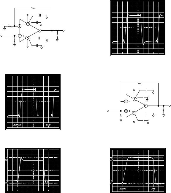
Figure 4. Test Circuit , Gain = +2
Figure 5. 1 V Step Response, G = +2 |
0.5V |
5ns |
Figure 6. 2 V Step Response, G = +1 |
|
400mV |
5ns |
Figure 7. 2 V Step Response, G = +2 |
|
|
|
909V |
|
|
+VS |
0.001mF |
|
|
|
|
VOUT TO |
|
|
|
TEKTRONIX |
|
|
|
CSA 404 COMM. |
|
|
|
SIGNAL |
|
|
|
ANALYZER |
|
AD8001 |
|
|
VIN |
|
0.1mF |
RL = 100V |
LeCROY 9210 |
50V |
|
|
PULSE |
0.001mF |
|
|
|
|
||
GENERATOR |
|
|
|
|
|
|
|
TR/TF = 350ps |
–V |
|
|
|
S |
|
|
Figure 8. Test Circuit, Gain = +1
Figure 9. 100 mV Step Response, G = +1 |
–4– |
REV. C |

GAIN – dB
|
|
|
|
|
|
|
|
|
AD8001 |
|
9 |
|
|
|
|
1000 |
|
|
|
|
|
|
|
|
|
|
|
|
|
|
|
|
6 |
VS = 65V |
|
|
VS = 65V |
|
|
|
|
||
R |
FB |
= 820V |
|
800 |
|
|
|
|
||
|
|
|
|
RL = 100V |
|
|
|
|||
|
|
|
|
MHz |
|
|
|
|||
3 |
G = +2 |
|
|
|
G = +2 |
|
|
|
|
|
RL = 100V |
|
|
– |
|
|
|
|
|
|
|
|
|
|
400 |
|
|
|
|
|
||
|
RFB = 1kV |
|
|
BANDWIDTH |
|
|
|
|
|
|
0 |
|
|
|
|
600 |
|
|
|
N |
|
|
|
|
|
|
|
|
|
|
PACKAGE |
|
–3 |
VS = 65V |
|
|
|
|
|
|
|
|
|
|
|
|
|
|
|
|
|
|
|
|
–6 |
|
|
|
–3dB |
|
|
R |
|
|
|
|
|
|
|
|
|
|
PACKAGE |
|
|
|
|
|
|
|
|
200 |
|
|
|
|
|
–9 |
|
|
|
|
|
|
|
|
|
|
–12 |
|
|
|
|
0 |
|
|
|
|
|
10M |
100M |
|
1G |
|
500 |
600 |
700 |
800 |
900 |
1000 |
FREQUENCY – Hz |
VALUE OF FEEDBACK RESISTOR (RF) –V |
|
|
Figure 10. Frequency Response, G = +2 |
||
|
0.1 |
|
RF = |
|
|
|
|
|
0 |
|
649V |
|
|
|
|
|
–0.1 |
|
RF = 698V |
|
|
|
|
dB |
–0.2 |
|
RF = 750V |
–0.3 |
|
|
|
– |
|
|
|
|
G = +2 |
|
|
OUTPUT |
|
|
|
–0.4 |
RL = 100V |
|
|
–0.5 |
VIN = 50mV |
|
|
|
|
||
|
|
|
|
|
–0.6 |
|
|
|
–0.7 |
|
|
|
–0.8 |
|
|
|
–0.9 |
|
|
|
1M |
10M |
100M |
FREQUENCY – Hz
Figure 11. 0.1 dB Flatness, R Package (for N Package Add |
|||||
50 Ω to RF) |
|
|
|
|
|
|
–50 |
|
|
|
|
|
|
VOUT = 2V p-p |
65V SUPPLIES |
|
|
|
–60 |
|
|
|
|
dBc |
RL = 1kV |
|
|
|
|
|
G = +2 |
|
|
|
|
– |
|
|
|
|
|
DISTORTION |
–70 |
2ND HARMONIC |
|
|
|
|
|
|
|||
–80 |
|
|
|
|
|
|
|
|
|
|
|
HARMONIC |
–90 |
|
3RD HARMONIC |
|
|
–100 |
|
|
|
|
|
|
|
|
|
|
|
|
–110 |
100k |
1M |
10M |
100M |
|
10k |
||||
|
|
|
FREQUENCY – Hz |
|
|
Figure 12. Distortion vs. Frequency, RL = 1 kΩ
Figure 13. –3 dB Bandwidth vs. RF
|
–50 |
|
|
|
|
|
|
|
65V SUPPLIES |
|
|
– dBc |
–60 |
VOUT = 2V p-p |
|
|
|
|
RL = 100V |
|
|
|
|
DISTORTION |
|
G = +2 |
|
|
|
–70 |
|
|
|
|
|
|
2ND HARMONIC |
|
|
||
|
|
|
|
|
|
HARMONIC |
–80 |
|
|
|
|
|
|
3RD HARMONIC |
|
||
–90 |
|
|
|
|
|
|
–100 |
100k |
1M |
10M |
100M |
|
10k |
||||
|
|
|
FREQUENCY – Hz |
|
|
|
Figure 14. Distortion vs. Frequency, RL = 100 Ω |
|||
Degrees |
0.08 |
|
|
|
0.06 |
G = +2 |
|||
RF |
= 806V |
|||
– |
|
|||
0.04 |
|
2 BACK TERMINATED |
||
PHASE |
|
|||
|
LOADS (75V) |
|||
0.02 |
|
|
||
DIFF |
0.00 |
|
|
|
|
|
1 BACK TERMINATED |
||
|
|
|
||
|
|
|
LOAD (150V) |
|
% |
0.02 |
|
|
|
|
|
1 AND 2 BACK TERMINATED |
||
– |
0.01 |
|
||
|
LOADS (150V AND 75V) |
|||
GAIN |
|
|
||
0.00 |
|
|
||
DIFF |
–0.01 |
|
|
|
|
|
|
||
|
–0.02 |
0 |
100 |
|
|
|
|||
|
|
|
IRE |
|
Figure 15. Differential Gain and Differential Phase
REV. C |
–5– |
 Loading...