


 Loading...
Analog Devices ADM1810-10AKS, ADM1810-10AKSZ, ADM1810-10ART, ADM1810-10ARTZ, ADM1810-5AKS Schematic [ru]
...Microprocessor Reset Circuits
ADM1810-ADM1813/ADM1815-ADM1818
FEATURES
Reliable low cost voltage monitor with reset output
Suitable for monitoring 2.5 V, 3 V, 3.3 V, and 5 V power supply voltages
Reset threshold levels: 4.62 V, 4.35 V, 3.06 V, 2.88 V, 2.55 V, 2.31 V, and 2.18 V typical
Active high and low push-pull output choices: ADM1810, ADM1812, ADM1815, and ADM1817
Open-drain output choices: ADM1811, ADM1813, ADM1816, and ADM1818
Can be used with a manual push-button to generate a reset: ADM1813, ADM1818
Initialization of microprocessor systems with added safety Available in 3-lead SOT-23 and SC70 packages
APPLICATIONS
Microprocessor systems
Computers
Controllers
Intelligent instruments
Automotive systems
GENERAL DESCRIPTION
The ADM181x range of voltage monitoring circuits is used in any application where an electronic system needs to be reset when a voltage increases above or below a predetermined value.
Because of the reset delay time incorporated into the ADM181x series, these devices provide a safe startup for electronic systems. Before a system initializes, the power supply must stabilize.
Using the ADM181x series ensures that there are typically 150 ms for the power supply to stabilize before the system resets and safe system initialization begins.
The ADM181x series of microprocessor reset circuits are available in low cost, space-saving SOT-23 and SC70 packages.
FUNCTIONAL BLOCK DIAGRAMS
VCC |
ADM1810/ADM1815 |
|
|
||
|
RST |
|
|
VCC |
|
|
TOLERANCE |
|
|
BIAS |
|
|
150ms |
|
|
DELAY |
|
GND |
TC |
|
REFERENCE |
||
|
||
VCC |
ADM1811/ADM1816 |
|
5.5kΩ |
||
|
||
|
RST |
VCC
|
TOLERANCE |
|
|
BIAS |
150ms |
|
|
|
|
|
DELAY |
GND |
TC |
|
REFERENCE |
|
|
|
|
|
VCC |
ADM1812/ADM1817 |
|
|
|
|
|
|
RST |
|
VCC |
|
|
TOLERANCE |
|
|
BIAS |
150ms |
|
|
|
|
|
DELAY |
GND |
TC |
|
REFERENCE |
|
|
|
|
|
VCC |
ADM1813/ADM1818 |
|
|
5.5kΩ |
|
|
RESET |
|
|
RST |
|
|
MONITOR |
|
|
|
|
|
|
VCC |
|
|
|
|
|
|
|
|
|
|
|
|
|
|
|
|
|
|
|
|
|
|
|
|
|
TOLERANCE |
|
|
|
|
|
|
|
|
|
|
|
|
BIAS |
|
|
|
150ms |
|
|
|||
|
|
|
|
|
|
|
|
|
||||
|
|
|
|
|
|
|
DELAY |
|
|
|||
GND |
|
|
TC |
001-00064 |
||||||||
|
|
|
|
|
|
|
|
|
|
|||
|
|
|
|
|
|
|
|
|
||||
|
|
|
REFERENCE |
|
|
|
|
|
||||
|
|
|
|
|
|
|
|
|
|
|
|
|
|
|
|
|
|
|
|
|
|
|
|
|
|
Figure 1.
Rev. D
Information furnished by Analog Devices is believed to be accurate and reliable. However, no responsibilityisassumedbyAnalogDevicesforitsuse,norforanyinfringementsofpatentsorother rightsofthirdpartiesthatmayresultfromitsuse.Specificationssubjecttochangewithoutnotice.No license is granted by implication or otherwise under any patent or patent rights of Analog Devices. Trademarksandregisteredtrademarksarethepropertyoftheirrespectiveowners.
One Technology Way, P.O. Box 9106, Norwood, MA 02062-9106, U.S.A.
Tel: 781.329.4700 |
www.analog.com |
Fax: 781.461.3113 |
© 2005 Analog Devices, Inc. All rights reserved. |

ADM1810-ADM1813/ADM1815-ADM1818
TABLE OF CONTENTS |
|
Features .............................................................................................. |
1 |
Applications....................................................................................... |
1 |
General Description ......................................................................... |
1 |
Functional Block Diagrams............................................................. |
1 |
Revision History ............................................................................... |
2 |
Specifications..................................................................................... |
3 |
Absolute Maximum Ratings............................................................ |
4 |
ESD Caution.................................................................................. |
4 |
Pin Configurations and Function Descriptions ........................... |
5 |
REVISION HISTORY |
|
10/05—Rev. C to Rev. D |
|
Updated Format.................................................................. |
Universal |
Added Figure 3................................................................................... |
5 |
Changes to Table 3............................................................................. |
5 |
Updated Outline Dimensions .......................................................... |
8 |
Changes to Ordering Guide ............................................................. |
9 |
9/03—REV. B to REV. C. |
|
Added SC70......................................................................... |
Universal |
Edits to SPECIFICATIONS.............................................................. |
2 |
Edits to ORDERING GUIDE........................................................... |
4 |
Updated OUTLINE DIMENSIONS ............................................... |
7 |
2/03—REV. A to REV. B. |
|
Edits to FEATURES........................................................................... |
1 |
Deleted Table I ................................................................................... |
1 |
Edits to SPECIFICATIONS.............................................................. |
2 |
Typical Performance Characteristics .............................................. |
6 |
Theory of Operation........................................................................... |
7 |
Timing Diagrams for All Devices ............................................... |
7 |
ADM1813 and ADM1818.............................................................. |
7 |
ADM1810, ADM1812, ADM1815, and ADM1817 ..................... |
7 |
ADM1811 and ADM1816.............................................................. |
7 |
Outline Dimensions .......................................................................... |
8 |
Ordering Guide ............................................................................. |
9 |
Edits to ABSOLUTE MAXIMUM RATINGS ............................... |
3 |
Edits to ORDERING GUIDE .......................................................... |
3 |
Added Typical Performance Characteristics ................................. |
4 |
Edits to ADM1813 AND ADM1818 section................................. |
5 |
Edits to ADM1810, ADM1812, ADM1815, AND |
|
ADM1817 section.............................................................................. |
5 |
Edits to ADM1811 AND ADM1816 section................................. |
5 |
Updated OUTLINE DIMENSIONS ............................................... |
6 |
3/02—REV. 0 to REV. A. |
|
Addition of Table .............................................................................. |
1 |
Edits to ORDERING GUIDE .......................................................... |
3 |
Addition of new text to ADM1813 and ADM1818 section......... |
4 |
Rev. D | Page 2 of 16

ADM1810-ADM1813/ADM1815-ADM1818
SPECIFICATIONS
VCC = full operating range, TA = −40°C to +105°C, unless otherwise noted.
Table 1.
Parameter |
Min |
Typ |
Max |
Unit |
Conditions/Note |
|||||
|
|
|
|
|
|
|
|
|
|
|
SUPPLY |
|
|
|
|
|
|||||
|
Voltage |
1 |
|
5.5 |
V |
TA = 0°C to 105°C |
||||
|
|
|
|
|
|
1.2 |
|
5.5 |
V |
TA = −40°C to +105°C |
|
Current |
|
9 |
16 |
μA |
VCC = 5.5 V, VCC > VTH, no load |
||||
|
|
|
|
|
|
|
4 |
10 |
μA |
VCC = 3.6 V, VCC > VTH, no load |
OUTPUT CURRENT |
|
|
|
|
|
|||||
|
|
|
|
|
|
350 |
|
μA |
VCC ≥ VTH (max), reset not asserted (ADM1810/ADM1815) |
|
|
RST |
Output Source Current |
|
|
||||||
|
RST Output Source Current |
|
350 |
|
μA |
VCC ≤ VTH (min), reset asserted (ADM1812/ADM1817) |
||||
|
|
|
|
8 |
|
|
mA |
VCC ≥ 2.7 V, reset asserted, VOUT = 0.4 V |
||
|
RST |
Output Sink Current |
|
|
||||||
|
|
|
|
|
|
|
|
|
|
(ADM1810/ADM1811/ADM1813/ |
|
|
|
|
|
|
|
|
|
|
ADM1815/ADM1816/ADM1818) |
|
RST Output Sink Current |
8 |
|
|
mA |
VCC ≥ 2.7 V, reset not asserted, |
||||
|
|
|
|
|
|
|
|
|
|
VOUT = 0.4 V (ADM1812/ADM1817) |
OUTPUT VOLTAGE |
VCC − 0.5 |
VCC − 0.1 |
|
V |
(ADM1810/ADM1812/ADM1815/ADM1817) |
|||||
|
|
|
|
|
|
|
|
|
|
@ 0 μA to 500 μA |
|
|
|
|
|
|
|
|
|||
VCC TRIP POINT |
|
|
|
|
|
|||||
|
ADM1810-5, ADM1811-5, ADM1812-5, |
4.50 |
4.62 |
4.75 |
V |
|
||||
|
ADM1813-5 |
|
|
|
|
|
||||
|
ADM1810-10, ADM1811-10, ADM1812-10, |
4.25 |
4.35 |
4.49 |
V |
|
||||
|
ADM1813-10 |
|
|
|
|
|
||||
|
ADM1815-5, ADM1816-5, ADM1817-5, |
2.98 |
3.06 |
3.15 |
V |
|
||||
|
ADM1818-5 |
|
|
|
|
|
||||
|
ADM1815-10, ADM1816-10, |
2.80 |
2.88 |
2.97 |
V |
|
||||
|
ADM1817-10, ADM1818-10 |
|
|
|
|
|
||||
|
ADM1815-20, ADM1816-20, |
2.47 |
2.55 |
2.64 |
V |
|
||||
|
ADM1817-20, ADM1818-20 |
|
|
|
|
|
||||
|
ADM1815-R23, ADM1816-R23, |
2.25 |
2.31 |
2.37 |
V |
|
||||
|
ADM1817-R23, ADM1818-R23 |
|
|
|
|
|
||||
|
ADM1815-R22, ADM1816-R22, |
2.12 |
2.18 |
2.25 |
V |
|
||||
|
ADM1817-R22, ADM1818-R22 |
|
|
|
|
|
||||
|
|
|
|
|
|
|
|
|||
INTERNAL PULL-UP RESISTOR |
|
|
|
|
|
|||||
|
ADM1811/ADM1816 |
3.5 |
5.5 |
7.5 |
kΩ |
|
||||
|
ADM1813/ADM1818 |
3.1 |
5.5 |
7.5 |
kΩ |
|
||||
OUTPUT CAPACITANCE |
|
|
10 |
pF |
|
|||||
RESET ACTIVE TIME |
100 |
150 |
250 |
ms |
|
|||||
|
|
|
|
|
|
|
|
|||
VCC DETECT TO RESET |
|
|
|
|
|
|||||
|
Falling |
|
10 |
|
μs |
(ADM1810/ADM1811/ADM1812/ADM1813) |
||||
|
|
|
|
|
|
|
10 |
|
μs |
(ADM1815/ADM1816/ADM1817/ADM1818) |
|
Rising |
100 |
150 |
250 |
ms |
tR = 5 μs |
||||
|
|
|
|
|
|
|||||
PUSH-BUTTON DETECT TO |
|
|
1 |
|
|
μs |
(ADM1813/ADM1818) |
|||
RST |
|
|
|
|||||||
|
|
|
|
|
|
|||||
PUSH-BUTTON RESET |
100 |
150 |
250 |
ms |
(ADM1813/ADM1818) |
|||||
|
|
|
|
|
|
|
|
|
|
|
Rev. D | Page 3 of 16

ADM1810-ADM1813/ADM1815-ADM1818
ABSOLUTE MAXIMUM RATINGS
TA = 25°C, unless otherwise noted.
Table 2.
Parameter |
Rating |
||
|
|
||
VCC |
−0.3 V to +6.0 V |
||
Input Current |
20 mA |
||
Operating Temperature Range |
−40°C to +105°C |
||
θ |
JA |
Thermal Impedance, SOT-23 |
270°C/W |
|
|
||
θ |
JA |
Thermal Impedance, SC70 |
146°C/W |
|
|
||
Lead Temperature (Soldering, 10 sec) |
300°C |
||
|
Vapor Phase (60 sec) |
215°C |
|
|
Infrared (15 sec) |
220°C |
|
Storage Temperature Range |
−65°C to +150°C |
||
|
|
|
|
Stresses above those listed under Absolute Maximum Ratings may cause permanent damage to the device. This is a stress rating only; functional operation of the device at these or any other conditions above those listed in the operational sections of this specification is not implied. Exposure to absolute maximum ratings for extended periods of time may affect device reliability.
ESD CAUTION
ESD (electrostatic discharge) sensitive device. Electrostatic charges as high as 4000 V readily accumulate on the human body and test equipment and can discharge without detection. Although this product features proprietary ESD protection circuitry, permanent damage may occur on devices subjected to high energy electrostatic discharges. Therefore, proper ESD precautions are recommended to avoid performance degradation or loss of functionality.
Rev. D | Page 4 of 16
ADM1810-ADM1813/ADM1815-ADM1818
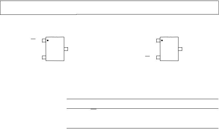
PIN CONFIGURATIONS AND FUNCTION DESCRIPTIONS
RST/RST 1 |
VCC 1 |
VCC 2
ADM181x
TOP VIEW 3 GND (Not to Scale)
002-00064
RST/RST 2
ADM181x
TOP VIEW 3 GND (Not to Scale)
014-00064
Figure 2. 3-Lead SOT Pin Configuration |
Figure 3. 3-Lead SC70 Pin Configuration |
Table 3. Pin Function Descriptions
Pin No. |
Pin No. |
|
|
|
(SOT) |
(SC70) |
|
Mnemonic |
|
1 |
2 |
|
|
|
|
RST/RST |
|||
2 |
1 |
|
VCC |
|
3 |
3 |
|
GND |
|
|
|
|
|
|
Function
Reset Output. RST/RST remains active while VCC is below the reset threshold and remains active for 150 ms typical after VCC rises above the reset threshold. Supply Voltage Being Monitored.
0 V Ground Reference for All Signals.
Rev. D | Page 5 of 16

ADM1810-ADM1813/ADM1815-ADM1818
TYPICAL PERFORMANCE CHARACTERISTICS
|
10 |
|
|
|
|
|
|
|
|
|
|
|
|
|
|
|
|
|
|
|
|
|
|
|
|
|
|
|
|
|
|
|
|
|
|
|
|
|
|
|
|
|
|
|
|
|
|
|
|
|
|
|
|
|
|
|
|
|
|
|
|
|
|
|
|
|
|
|
|
|
|
|
|
|
|
8 |
|
|
|
|
|
I |
CC @VCC = 5.5V |
|
|
|
|
|
|
|
|
|
|
|
|
|
|||
|
|
|
|
|
|
|
|
|
|
|
|
|
|
|
|
|
|
|
|
|
|
|
|
|
|
|
|
|
|
|
|
|
|
|
|
|
|
|
|
|
|
|
|
|
|
|
|
|
|
(μA) |
6 |
|
|
|
|
|
|
|
|
|
|
|
|
|
|
|
|
|
|
|
|
|
|
|
|
|
|
|
|
|
|
|
|
|
|
|
|
|
|
|
|
|
|
|
|
|
|
||
|
|
|
|
|
|
|
|
|
|
|
|
|
|
ICC @VCC = 3V |
|
|
|
|
||||||
CC |
|
|
|
|
|
|
|
|
|
|
|
|
|
|
|
|
|
|
|
|
|
|
|
|
I |
4 |
|
|
|
|
|
|
|
|
|
|
|
|
|
|
|
|
|
|
|
|
|
|
|
|
|
|
|
|
|
|
|
|
|
|
|
|
|
|
|
|
|
|
|
|
|
|
|
|
|
|
|
|
|
|
|
|
|
|
|
|
|
|
|
|
|
|
|
|
|
|
|
|
|
|
2 |
|
|
|
|
|
|
|
|
|
|
|
|
|
|
|
|
|
|
|
|
|
|
00064-003 |
|
|
|
|
|
|
|
|
|
|
|
|
|
|
|
|
|
|
|
|
|
|
|
||
|
0 |
|
|
|
|
|
|
|
|
|
|
|
|
|
|
|
|
|
|
|
|
|
|
|
|
|
–20 |
0 |
20 |
30 |
|
50 |
70 |
85 |
100 |
120 |
|
||||||||||||
|
–40 |
|
|
|||||||||||||||||||||
TEMPERATURE (°C)
Figure 4. Supply Current vs. Temperature
|
900 |
|
|
|
|
|
|
|
|
|
(μs) |
800 |
|
|
|
|
|
|
|
|
|
700 |
|
|
|
|
|
|
|
|
|
|
DELAY |
|
|
|
|
|
|
|
|
|
|
600 |
|
|
|
|
|
|
|
|
|
|
|
|
|
|
|
|
|
|
|
|
|
RESET |
500 |
|
|
|
|
|
VOD = 20mV |
|
|
|
400 |
|
|
|
|
|
|
|
|||
POWER-DOWN |
|
|
|
|
|
|
|
|
|
|
300 |
|
|
|
|
|
|
|
|
|
|
200 |
VOD = 125mV |
|
|
|
|
|
|
|
||
|
|
|
|
|
|
|
|
|
||
|
|
|
|
|
|
|
|
|
|
|
|
100 |
|
|
|
|
|
|
|
|
00064-004 |
|
0 |
|
|
|
|
VOD = 200mV |
|
|||
|
|
|
|
|
|
|
|
|
||
|
–20 |
0 |
20 |
30 |
50 |
70 |
85 |
100 |
120 |
|
|
–40 |
|||||||||
TEMPERATURE (°C)
Figure 5. Power-Down Reset Delay vs. Temperature
|
380 |
|
|
|
|
|
|
|
|
|
|
370 |
|
|
|
|
|
|
|
|
|
(ms) |
360 |
|
|
|
|
|
|
|
|
|
TIMEOUT |
350 |
|
|
|
|
|
|
|
|
|
340 |
|
|
|
|
|
|
|
|
|
|
RESET |
|
|
|
|
|
|
|
|
|
|
330 |
|
|
|
|
|
|
|
|
|
|
|
|
|
|
|
|
|
|
|
|
|
POWER-UP |
320 |
|
|
|
|
|
|
|
|
|
310 |
|
|
|
|
|
|
|
|
|
|
|
|
|
|
|
|
|
|
|
|
|
|
300 |
|
|
|
|
|
|
|
|
00064-005 |
|
290 |
|
|
|
|
|
|
|
|
|
|
–20 |
0 |
20 |
30 |
50 |
70 |
85 |
100 |
120 |
|
|
–40 |
TEMPERATURE (°C)
Figure 6. Power-Up Reset Timeout vs. Temperature
|
1.011 |
|
|
|
|
|
|
|
|
|
THRESHOLD |
1.009 |
|
|
|
|
|
|
|
|
|
1.007 |
|
|
|
|
|
|
|
|
|
|
1.005 |
|
|
|
DEVIATION (RISE) |
|
|
|
|||
RESET |
|
|
|
|
|
|
|
|||
1.003 |
|
|
|
|
|
|
|
|
|
|
|
DEVIATION (FALL) |
|
|
|
|
|
||||
NORMALIZED |
1.001 |
|
|
|
|
|
||||
|
|
|
|
|
|
|
|
|
||
0.999 |
|
|
|
|
|
|
|
|
|
|
0.997 |
|
|
|
|
|
|
|
|
|
|
|
|
|
|
|
|
|
|
|
00064-006 |
|
|
0.995 |
|
|
|
|
|
|
|
|
|
|
–20 |
0 |
20 |
30 |
50 |
70 |
85 |
100 |
120 |
|
|
–40 |
|||||||||
TEMPERATURE (°C)
Figure 7. Normalized Reset Threshold vs. Temperature
|
60 |
|
|
|
|
|
|
|
|
|
|
|
50 |
|
|
|
|
|
|
|
|
|
|
(μs) |
40 |
|
|
|
|
|
|
|
|
|
|
TRANSIENT |
|
|
|
|
|
|
|
|
|
|
|
30 |
|
|
|
|
|
|
|
|
|
|
|
|
|
|
|
|
|
|
|
|
|
|
|
MAXIMUM |
20 |
|
|
|
|
|
|
|
|
|
|
|
|
|
|
|
|
|
|
|
|
|
|
|
10 |
|
|
|
|
|
|
|
|
|
00064-007 |
|
0 |
|
|
|
|
|
|
|
|
|
|
|
30 |
40 |
60 |
80 |
100 |
200 |
400 |
600 |
800 |
1000 |
|
|
10 |
VTH – VCC (mV)
Figure 8. Maximum Transient Duration Without Causing a Reset Pulse vs. Reset Comparator Overdrive
Rev. D | Page 6 of 16
Loading...