


 Loading...
3 MSPS, 12-/10-/8-Bit
ADCs in 6-Lead TSOT
AD7276/AD7277/AD7278
FEATURES |
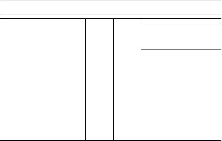
FUNCTIONAL BLOCK DIAGRAM |
Throughput rate: 3 MSPS Specified for VDD of 2.35 V to 3.6 V Power consumption
12.6 mW at 3 MSPS with 3 V supplies Wide input bandwidth
70 dB SNR at 1 MHz input frequency Flexible power/serial clock speed management No pipeline delays
High speed serial interface SPI®-/QSPI™-/MICROWIRE™-/DSP-compatible
Temperature range: −40°C to +125°C Power-down mode: 0.1 μA typical 6-lead TSOT package
8-lead MSOP package
AD7476 and AD7476A pin-compatible
VDD
|
|
12-/10-/8-BIT |
|
VIN |
T/H |
SUCCESSIVE |
|
APPROXIMATION |
|
||
|
|
ADC |
|
|
|
|
SCLK |
|
AD7276/ |
CONTROL |
SDATA |
|
AD7277/ |
LOGIC |
|
|
AD7278 |
|
CS |
|
|
GND |
04903-001 |
GENERAL DESCRIPTION
Figure 1.
Table 1.
The AD7276/AD7277/AD7278 are 12-/10-/8-bit, high speed, |
|
|
|
|
|
||
Part Number |
Resolution |
Package |
|||||
MacshbM |
|||||||
low power, successive approximation analog-to-digital |
AD7276 |
12 |
8-Lead MSOP |
6-Lead TSOT |
|||
converters (ADCs), respectively. The parts operate from single |
AD7277 |
10 |
8-Lead MSOP |
6-Lead TSOT |
|||
2.35 V to 3.6 V power supply and feature throughput rates of up |
|||||||
AD7278 |
8 |
8-Lead MSOP |
6-Lead TSOT |
||||
to 3 MSPS. The parts contain a low noise, wide bandwidth |
|||||||
AD72741 |
12 |
8-Lead MSOP |
8-Lead TSOT |
||||
track-and-hold amplifier that can handle input frequencies in |
AD72731 |
10 |
8-Lead MSOP |
8-Lead TSOT |
|||
excess of 55 MHz. |
|
|
|
|
|
|
|
|
|
|
|
|
|
||
The conversion process and data acquisition are controlled using CS and the serial clock, allowing the devices to interface with microprocessors or DSPs. The input signal is sampled on the falling edge of CS, and the conversion is also initiated at this point. There are no pipeline delays associated with the part.
The AD7276/AD7277/AD7278 use advanced design techniques to achieve very low power dissipation at high throughput rates.
The reference for the part is taken internally from VDD. This allows the widest dynamic input range to the ADC; therefore, the analog input range for the part is 0 to VDD. The conversion rate is determined by the SCLK.
Rev. A
Information furnished by Analog Devices is believed to be accurate and reliable. However, no responsibilityisassumedbyAnalogDevicesforitsuse,norforanyinfringementsofpatentsorother rightsofthirdpartiesthatmayresultfromitsuse.Specificationssubjecttochangewithoutnotice.No license is granted by implication or otherwise under any patent or patent rights of Analog Devices. Trademarksandregisteredtrademarksarethepropertyoftheirrespectiveowners.
1 Part contains external reference pin.
PRODUCT HIGHLIGHTS
1.3 MSPS ADCs in a 6-lead TSOT package.
2.AD7476/AD7477/AD7478 and AD7476A/AD7477A/ AD7478A pin-compatible.
3.High throughput with low power consumption.
4.Flexible power/serial clock speed management. This allows maximum power efficiency at low throughput rates.
5.Reference derived from the power supply.
6.No pipeline delay. The parts feature a standard successive approximation ADC with accurate control of the sampling instant via a CS input and once-off conversion control.
One Technology Way, P.O. Box 9106, Norwood, MA 02062-9106, U.S.A.
Tel: 781.329.4700 |
www.analog.com |
Fax: 781.461.3113 |
© 2005 Analog Devices, Inc. All rights reserved. |

AD7276/AD7277/AD7278
TABLE OF CONTENTS
Features .............................................................................................. |
|
1 |
Theory of Operation ...................................................................... |
16 |
General Description ......................................................................... |
1 |
Circuit Information.................................................................... |
16 |
|
Functional Block Diagram .............................................................. |
1 |
Converter Operation.................................................................. |
16 |
|
Product Highlights ........................................................................... |
1 |
ADC Transfer Function............................................................. |
16 |
|
Specifications..................................................................................... |
|
3 |
Typical Connection Diagram ................................................... |
16 |
AD7276 Specifications................................................................. |
3 |
Modes of Operation ................................................................... |
18 |
|
AD7277 Specifications................................................................. |
5 |
Power vs. Throughput Rate....................................................... |
21 |
|
AD7278 Specifications................................................................. |
7 |
Serial Interface ................................................................................ |
22 |
|
Timing Specifications—AD7276/AD7277/AD7278 ............... |
8 |
AD7278 in a 10 SCLK Cycle Serial Interface.......................... |
24 |
|
Timing Examples........................................................................ |
10 |
Microprocessor Interfacing....................................................... |
24 |
|
Absolute Maximum Ratings.......................................................... |
11 |
Application Hints ........................................................................... |
25 |
|
ESD Caution................................................................................ |
11 |
Grounding and Layout .............................................................. |
25 |
|
Pin Configurations and Function Descriptions ......................... |
12 |
Evaluating Performance.............................................................. |
25 |
|
Typical Performance Characteristics ........................................... |
13 |
Outline Dimensions ....................................................................... |
26 |
|
Terminology |
MacshbM |
|||
|
15 |
Ordering Guide .......................................................................... |
26 |
|
REVISION HISTORY |
|
|
|
|
10/05—Rev. 0 to Rev. A |
|
|
|
|
Updated Format.................................................................. |
Universal |
|
|
|
Changes to Table 2............................................................................ |
3 |
|
|
|
Changes to Table 5............................................................................ |
8 |
|
|
|
Changes to the Partial Power-Down Mode Section .................. |
18 |
|
|
|
Changes to the Power vs. Throughput Rate Section.................. |
21 |
|
|
|
Updated Outline Dimensions ....................................................... |
26 |
|
|
|
Changes to Ordering Guide .......................................................... |
26 |
|
|
|
7/05—Revision 0: Initial Version
Rev. A | Page 2 of 28

AD7276/AD7277/AD7278
SPECIFICATIONS
AD7276 SPECIFICATIONS
VDD = 2.35 V to 3.6 V, B Grade: fSCLK = 48 MHz, fSAMPLE = 3 MSPS, Y Grade:1 fSCLK = 16 MHz, fSAMPLE = 1 MSPS, TA = TMIN to TMAX, unless otherwise noted.
Table 2.
Parameter |
B, Y Grade2, 3 |
Unit |
Test Conditions/Comments |
DYNAMIC PERFORMANCE |
|
|
fIN = 1 MHz sine wave, B Grade |
|
|
|
fIN = 100 KHz sine wave, Y Grade |
Signal-to-Noise + Distortion (SINAD)4 |
68 |
dB min |
|
Signal-to-Noise Ratio (SNR) |
69 |
dB min |
|
|
70 |
dB typ |
|
Total Harmonic Distortion (THD)4 |
−73 |
dB max |
|
|
−78 |
dB typ |
|
Peak Harmonic or Spurious Noise (SFDR)4 |
−80 |
dB typ |
|
Intermodulation Distortion (IMD)4 |
|
|
|
Second-Order Terms |
−82 |
dB typ |
fa = 1 MHz, fb = 0.97 MHz |
Third-Order Terms |
−82 |
dB typ |
fa = 1 MHz, fb = 0.97 MHz |
Aperture Delay |
5 |
ns typ |
|
Aperture Jitter |
18 |
ps typ |
|
Full Power Bandwidth |
55 |
MHz typ |
@ 3 dB |
|
8 |
MHz typ |
@ 0.1 dB |
|
|
|
|
DC ACCURACY |
|
|
|
Resolution |
12 |
Bits |
|
|
±1 |
MacshbM |
|
Integral Nonlinearity4 |
LSB max |
|
|
Differential Nonlinearity4 |
+1/−0.99 |
LSB max |
Guaranteed no missed codes to 12 its |
Offset Error4 |
±3 |
LSB max |
|
Gain Error4 |
±3.5 |
LSB max |
|
Total Unadjusted Error4 (TUE) |
±3.5 |
LSB max |
|
ANALOG INPUT |
|
|
|
Input Voltage Ranges |
0 to VDD |
V |
|
DC Leakage Current |
±1 |
μA max |
−40°C to +85°C |
|
±5.5 |
μA max |
85°C to 125°C |
Input Capacitance |
42 |
pF typ |
When in track |
|
10 |
pF typ |
When in hold |
LOGIC INPUTS |
|
|
|
Input High Voltage, VINH |
1.7 |
V min |
2.35 V ≤ VDD ≤ 2.7 V |
|
2 |
V min |
2.7 V < VDD ≤ 3.6 V |
Input Low Voltage, VINL |
0.7 |
V max |
2.35 V ≤ VDD ≤ 2.7 V |
|
0.8 |
V max |
2.7 V < VDD ≤ 3.6 V |
Input Current, IIN |
±1 |
μA max |
Typically 10 nA, VIN = 0 V or VDD |
Input Capacitance, CIN5 |
2 |
pF typ |
|
LOGIC OUTPUTS |
|
|
|
Output High Voltage, VOH |
VDD – 0.2 |
V min |
ISOURCE = 200 μA, VDD = 2.35 V to 3.6 V |
Output Low Voltage, VOL |
0.2 |
V max |
ISINK = 200 μA |
Floating-State Leakage Current |
±2.5 |
μA max |
|
Floating-State Output Capacitance5 |
4.5 |
pF typ |
|
Output Coding |
Straight (natural) binary |
|
|
|
|
|
|
Rev. A | Page 3 of 28
AD7276/AD7277/AD7278
Parameter |
B, Y Grade2, 3 |
Unit |
Test Conditions/Comments |
CONVERSION RATE |
|
|
|
Conversion Time |
291 |
ns max |
14 SCLK cycles with SCLK at 48 MHz, B Grade |
|
875 |
ns max |
14 SCLK cycles with SCLK at 16 MHz, Y Grade |
Track-and-Hold Acquisition Time4 |
60 |
ns min |
|
Throughput Rate |
3 |
MSPS max |
See the Serial Interface section |
POWER REQUIREMENTS |
|
|
|
VDD |
2.35/3.6 |
V min/max |
|
IDD |
|
|
Digital I/Ps 0 V or VDD |
Normal Mode (Static) |
1 |
mA typ |
VDD = 3.6 V, SCLK on or off |
Normal Mode (Operational) |
5.5 |
mA max |
VDD = 2.35 V to 3.6 V, fSAMPLE = 3 MSPS, B Grade |
|
2.5 |
mA max |
VDD = 2.35 V to 3.6 V, fSAMPLE = 1 MSPS, Y Grade |
|
4.2 |
mA typ |
VDD = 3 V, fSAMPLE = 3 MSPS, B Grade |
|
1.6 |
mA typ |
VDD = 3 V, fSAMPLE = 1 MSPS, Y Grade |
Partial Power-Down Mode (Static) |
34 |
μA typ |
|
Full Power-Down Mode (Static) |
2 |
μA max |
−40°C to +85°C, typically 0.1 μA |
|
10 |
μA max |
85°C to 125°C |
Power Dissipation6 |
|
|
|
Normal Mode (Operational) |
19.8 |
mW max |
VDD = 3.6 V, fSAMPLE = 3 MSPS, B Grade |
|
9 |
mW max |
VDD = 3.6 V, fSAMPLE = 1 MSPS, Y Grade |
|
12.6 |
mW typ |
VDD = 3 V, fSAMPLE = 3 MSPS, B Grade |
|
4.8 |
mW typ |
VDD = 3 V, fSAMPLE = 1 MSPS, Y Grade |
Partial Power-Down |
102 |
μW typ |
VDD = 3 V |
Full Power-Down |
7.2 |
μW max |
VDD = 3.6 V, −40°C to +85°C |
1 Y Grade specifications are guaranteed by characterization. MacshbM 2 Temperature range from −40°C to +125°C.
3 Typical specifications are tested with VDD = 3 V and at 25°C. 4 See the Terminology section.
5 Guaranteed by characterization.
6 See the Power vs. Throughput Rate section.
Rev. A | Page 4 of 28

AD7276/AD7277/AD7278
AD7277 SPECIFICATIONS
VDD = 2.35 V to 3.6 V, fSCLK = 48 MHz, fSAMPLE = 3 MSPS, TA = TMIN to TMAX, unless otherwise noted.
Table 3.
Parameter |
B Grade1, 2 |
Unit |
Test Conditions/Comments |
DYNAMIC PERFORMANCE |
|
|
fIN = 1 MHz sine wave |
Signal-to-Noise + Distortion (SINAD)3 |
60.5 |
dB min |
|
Total Harmonic Distortion (THD)3 |
−71 |
dB max |
|
|
−76 |
dB typ |
|
Peak Harmonic or Spurious Noise (SFDR)3 |
−80 |
dB typ |
|
Intermodulation Distortion (IMD)3 |
|
|
|
Second-Order Terms |
−82 |
dB typ |
fa = 1 MHz, fb = 0.97 MHz |
Third-Order Terms |
−82 |
dB typ |
fa = 1 MHz, fb = 0.97 MHz |
Aperture Delay |
5 |
ns typ |
|
Aperture Jitter |
18 |
ps typ |
|
Full Power Bandwidth |
74 |
MHz typ |
@ 3 dB |
|
10 |
MHz typ |
@ 0.1 dB |
|
|
|
|
DC ACCURACY |
|
|
|
Resolution |
10 |
Bits |
|
Integral Nonlinearity3 |
±0.5 |
LSB max |
|
Differential Nonlinearity3 |
±0.5 |
LSB max |
Guaranteed no missed codes to 10 bits |
Offset Error3 |
±1 |
LSB max |
|
Gain Error3 |
±1.5 |
LSB max |
|
Total Unadjusted Error (TUE)3 |
±2.5 |
LSB max |
|
|
±5.5 |
MacshbMμA max 85°C to 125°C |
|
ANALOG INPUT |
|
|
|
Input Voltage Ranges |
0 to VDD |
V |
|
DC Leakage Current |
±1 |
μA max |
−40°C to +85°C |
Input Capacitance |
42 |
pF typ |
When in track |
|
10 |
pF typ |
When in hold |
LOGIC INPUTS |
|
|
|
Input High Voltage, VINH |
1.7 |
V min |
2.35 V ≤ VDD ≤ 2.7 V |
|
2 |
V min |
2.7 V < VDD ≤ 3.6 V |
Input Low Voltage, VINL |
0.7 |
V max |
2.35 V ≤ VDD ≤ 2.7 V |
|
0.8 |
V max |
2.7 V < VDD ≤ 3.6 V |
Input Current, IIN |
±1 |
μA max |
Typically 10 nA, VIN = 0 V or VDD |
Input Capacitance, CIN4 |
2 |
pF typ |
|
LOGIC OUTPUTS |
|
|
|
Output High Voltage, VOH |
VDD − 0.2 |
V min |
ISOURCE = 200 μA, VDD = 2.35 V to 3.6 V |
Output Low Voltage, VOL |
0.2 |
V max |
ISINK = 200 μA |
Floating-State Leakage Current |
±2.5 |
μA max |
|
Floating-State Output Capacitance4 |
4.5 |
pF typ |
|
Output Coding |
Straight (natural) binary |
|
|
|
|
|
|
CONVERSION RATE |
|
|
|
Conversion Time |
250 |
ns max |
12 SCLK cycles with SCLK at 48 MHz |
Track-and-Hold Acquisition Time3 |
60 |
ns min |
|
Throughput Rate |
3.45 |
MSPS max |
SCLK at 48 MHz |
Rev. A | Page 5 of 28

AD7276/AD7277/AD7278
Parameter |
B Grade1, 2 |
Unit |
Test Conditions/Comments |
|
POWER REQUIREMENTS |
|
|
|
|
|
VDD |
2.35/3.6 |
V min/max |
|
|
IDD |
|
|
Digital I/Ps 0 V or VDD |
|
Normal Mode (Static) |
0.6 |
mA typ |
VDD = 3.6 V, SCLK on or off |
|
Normal Mode (Operational) |
5.5 |
mA max |
VDD = 2.35 V to 3.6 V, fSAMPLE = 3 MSPS |
|
|
3.5 |
mA typ |
VDD = 3 V |
|
Partial Power-Down Mode (Static) |
34 |
μA typ |
|
|
Full Power-Down Mode (Static) |
2 |
μA max |
−40°C to +85°C, typically 0.1 μA |
|
|
10 |
μA max |
85°C to 125°C |
|
Power Dissipation5 |
|
|
|
|
Normal Mode (Operational) |
19.8 |
mW max |
VDD = 3.6 V, fSAMPLE = 3 MSPS |
|
|
10.5 |
mW typ |
VDD = 3 V |
|
Partial Power-Down |
102 |
μW typ |
VDD = 3 V |
|
Full Power-Down |
7.2 |
μW max |
VDD = 3.6 V, −40°C to +85°C |
|
|
|
|
|
1 |
Temperature range from −40°C to +125°C. |
|
|
|
2 |
Typical specifications are tested with VDD = 3 V and at 25°C. |
|
|
|
3 |
See the Terminology section. |
|
|
|
4 |
Guaranteed by characterization. |
|
|
|
5 |
See the Power vs. Throughput Rate section. |
|
|
|
MacshbM
Rev. A | Page 6 of 28

AD7276/AD7277/AD7278
AD7278 SPECIFICATIONS
VDD = 2.35 V to 3.6 V, fSCLK = 48 MHz, fSAMPLE = 3 MSPS, TA = TMIN to TMAX, unless otherwise noted.
Table 4.
Parameter |
B Grade1, 2 |
Unit |
Test Conditions/Comments |
|
|
DYNAMIC PERFORMANCE |
|
|
fIN = 1 MHz sine wave |
||
Signal-to-Noise + Distortion (SINAD)3 |
49 |
dB min |
|
|
|
Total Harmonic Distortion (THD)3 |
−67 |
dB max |
|
|
|
|
−73 |
dB typ |
|
|
|
Peak Harmonic or Spurious Noise (SFDR)3 |
−69 |
dB typ |
|
|
|
Intermodulation Distortion (IMD)3 |
|
|
|
|
|
Second-Order Terms |
−76 |
dB typ |
fa = 1 MHz, fb = 0.97 MHz |
||
Third-Order Terms |
−76 |
dB typ |
fa = 1 MHz, fb = 0.97 MHz |
||
Aperture Delay |
5 |
ns typ |
|
|
|
Aperture Jitter |
18 |
ps typ |
|
|
|
Full Power Bandwidth |
74 |
MHz typ |
@ 3 dB |
||
Full Power Bandwidth |
10 |
MHz typ |
@ 0.1 dB |
||
|
|
|
|
|
|
DC ACCURACY |
|
|
|
|
|
Resolution |
8 |
Bits |
|
|
|
Integral Nonlinearity3 |
±0.2 |
LSB max |
|
|
|
Differential Nonlinearity3 |
±0.3 |
LSB max |
Guaranteed no missed codes to 8 bits |
||
Offset Error3 |
±0.5 |
LSB max |
|
|
|
Gain Error3 |
±1 |
LSB max |
|
|
|
Total Unadjusted Error (TUE)3 |
±1.5 |
LSB max |
|
|
|
|
±5.5 |
MacshbMμA max 85°C to 125°C |
|
|
|
ANALOG INPUT |
|
|
|
|
|
Input Voltage Ranges |
0 to VDD |
V |
|
|
|
DC Leakage Current |
±1 |
μA max |
−40°C to +85°C |
||
Input Capacitance |
42 |
pF typ |
When in track |
||
|
10 |
pF typ |
When in hold |
||
LOGIC INPUTS |
|
|
|
|
|
Input High Voltage, VINH |
1.7 |
V min |
2.35 V ≤ VDD ≤ 2.7 V |
||
|
2 |
V min |
2.7 V < VDD ≤ 3.6 V |
||
Input Low Voltage, VINL |
0.7 |
V max |
2.35 V ≤ VDD ≤ 2.7 V |
||
|
0.8 |
V max |
2.7 V < VDD ≤ 3.6 V |
||
Input Current, IIN |
±1 |
μA max |
|
|
|
Input Capacitance, CIN4 |
2 |
pF typ |
|
|
|
LOGIC OUTPUTS |
|
|
|
|
|
Output High Voltage, VOH |
VDD – 0.2 |
V min |
ISOURCE = 200 μA, VDD = 2.35 V to 3.6 V |
||
Output Low Voltage, VOL |
0.2 |
V max |
ISINK = 200 μA |
||
Floating-State Leakage Current |
±2.5 |
μA max |
|
|
|
Floating-State Output Capacitance4 |
4.5 |
pF typ |
|
|
|
Output Coding |
Straight (natural) binary |
|
|
|
|
|
|
|
|
|
|
CONVERSION RATE |
|
|
|
|
|
Conversion Time |
208 |
ns max |
10 SCLK cycles with SCLK at 48 MHz |
||
Track-and-Hold Acquisition Time3 |
60 |
ns min |
|
|
|
Throughput Rate |
4 |
MSPS max |
SCLK at 48 MHz |
|
|
Rev. A | Page 7 of 28

AD7276/AD7277/AD7278
Parameter |
B Grade1, 2 |
Unit |
Test Conditions/Comments |
|
POWER REQUIREMENTS |
|
|
|
|
|
VDD |
2.35/3.6 |
V min/max |
|
|
IDD |
|
|
Digital I/Ps = 0 V or VDD |
|
Normal Mode (Static) |
0.5 |
mA typ |
VDD = 3.6 V, SCLK on or off |
|
Normal Mode (Operational) |
5.5 |
mA max |
VDD = 2.35 V to 3.6 V, fSAMPLE = 3 MSPS |
|
|
3.5 |
mA typ |
VDD = 3 V |
|
Partial Power-Down Mode (Static) |
34 |
μA typ |
|
|
Full Power-Down Mode (Static) |
2 |
μA max |
−40°C to +85°C, typically 0.1 μA |
|
|
10 |
μA max |
+85°C to +125°C |
|
Power Dissipation5 |
|
|
|
|
Normal Mode (Operational) |
19.8 |
mW max |
VDD = 3.6 V, fSAMPLE = 3 MSPS |
|
|
10.5 |
mW typ |
VDD = 3 V |
|
Partial Power-Down |
102 |
μW typ |
VDD = 3 V |
|
Full Power-Down |
7.2 |
μW max |
VDD = 3.6 V, −40°C to +85°C |
1 |
Temperature range from −40°C to +125°C. |
|
|
|
2 |
Typical specifications are tested with VDD = 3 V and at 25°C. |
|
|
|
3 |
See the Terminology section. |
|
|
|
4 |
Guaranteed by characterization. |
|
|
|
5 |
See the Power vs. Throughput Rate section. |
|
|
|
TIMING SPECIFICATIONS—AD7276/AD7277/AD7278
VDD = 2.35 V to 3.6 V, TA = TMIN to TMAX, unless otherwise noted.1
fSCLK |
|
48500 MHzkHz minmaxMacshbMB gr de |
|||||||||
Table 5. |
|
|
|
|
|
|
|
|
|
|
|
Parameter2 |
Limit at TMIN, TMAX |
Unit |
|
Description |
|||||||
|
3 |
|
4 |
|
|
|
|
|
|
|
|
|
|
16 |
MHz max |
Y grade |
|||||||
tCONVERT |
14 × tSCLK |
|
|
AD7276 |
|||||||
|
|
12 × tSCLK |
|
|
AD7277 |
||||||
|
|
10 × tSCLK |
|
|
AD7278 |
||||||
tQUIET |
4 |
ns min |
|
Minimum quiet time required between the bus relinquish and the |
|||||||
|
|
|
|
|
start of the next conversion |
||||||
t1 |
|
3 |
ns min |
|
|
|
|
|
|
||
|
|
Minimum |
CS |
pulse width |
|||||||
t2 |
|
6 |
ns min |
|
|
|
|
|
|||
|
|
CS |
to SCLK setup time |
||||||||
t35 |
|
4 |
ns max |
|
|
|
|||||
|
|
Delay from |
CS |
until SDATA three-state disabled |
|||||||
t45 |
|
15 |
ns max |
|
Data access time after SCLK falling edge |
||||||
t5 |
|
0.4 tSCLK |
ns min |
|
SCLK low pulse width |
||||||
t6 |
|
0.4 tSCLK |
ns min |
|
SCLK high pulse width |
||||||
t75 |
|
5 |
ns min |
|
SCLK to data valid hold time |
||||||
t8 |
|
14 |
ns max |
|
SCLK falling edge to SDATA three-state |
||||||
|
|
5 |
ns min |
|
SCLK falling edge to SDATA three-state |
||||||
t9 |
|
4.2 |
ns max |
|
|
|
|||||
|
|
CS |
rising edge to SDATA three-state |
||||||||
TPOWER-UP6 |
1 |
μs max |
|
Power-up time from full power-down |
|
||||||
1 Sample tested during initial release to ensure compliance. All timing specifications given are with a 10 pF load capacitance. With a load capacitance greater than this value, a digital buffer or latch must be used.
2 Guaranteed by characterization. All input signals are specified with tr = tf = 2 ns (10% to 90% of VDD) and timed from a voltage level of 1.6 V. 3 Mark/space ratio for the SCLK input is 40/60 to 60/40.
4 Minimum fSCLK at which specifications are guaranteed.
5 The time required for the output to cross the VIH or VIL voltage. 6 See the Power-Up Times section.
Rev. A | Page 8 of 28
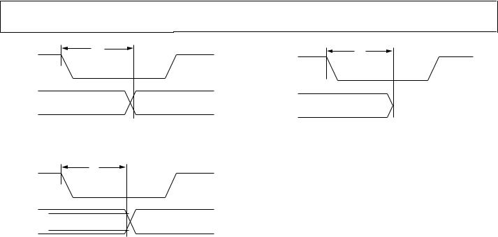
t4
SCLK
SDATA |
|
VIH |
-002 |
|
|||
|
|
VIL |
04903 |
|
|
|
Figure 2. Access Time After SCLK Falling Edge
|
t7 |
SCLK |
|
VIH |
-003 |
SDATA |
|
VIL |
04903 |
Figure 3. Hold Time After SCLK Falling Edge
AD7276/AD7277/AD7278
t8
SCLK
|
1.4V |
|
SDATA |
|
004-04903 |
|
|
|
Figure 4. SCLK Falling Edge SDATA Three-State
MacshbM
Rev. A | Page 9 of 28
Loading...