


Analog Devices AD7845SE-883B, AD7845AQ, AD7845KR, AD7845KP, AD7845KN Datasheet
...
a |
LC2MOS |
|
Complete 12-Bit Multiplying DAC |
||
|
|
|
|
|
AD7845 |
|
|
|
FEATURES
12-Bit CMOS MDAC with Output Amplifier
4-Quadrant Multiplication
Guaranteed Monotonic (TMIN to TMAX)
Space-Saving 0.3" DIPs and 24or 28-Terminal Surface Mount Packages
Application Resistors On Chip for Gain Ranging, etc. Low Power LC2MOS
APPLICATIONS
Automatic Test Equipment
Digital Attenuators
Programmable Power Supplies
Programmable Gain Amplifiers
Digital-to-4–20 mA Converters
GENERAL DESCRIPTION
The AD7845 is the industry’s first 4-quadrant multiplying D/A converter with an on-chip amplifier. It is fabricated on the LC2MOS process, which allows precision linear components and digital circuitry to be implemented on the same chip.
The 12 data inputs drive latches which are controlled by standard CS and WR signals, making microprocessor interfacing simple. For stand-alone operation, the CS and WR inputs can be tied to ground, making all latches transparent. All digital inputs are TTL and 5 V CMOS compatible.
The output amplifier can supply ± 10 V into a 2 kΩ load. It is internally compensated, and its input offset voltage is low due to laser trimming at wafer level. For normal operation, RFB is tied
to VOUT, but the user may alternatively choose RA, RB or RC to scale the output voltage range.
FUNCTIONAL BLOCK DIAGRAM
PRODUCT HIGHLIGHTS
1.Voltage Output Multiplying DAC
The AD7845 is the first DAC which has a full 4-quadrant multiplying capability and an output amplifier on chip. All specifications include amplifier performance.
2.Matched Application Resistors
Three application resistors provide an easy facility for gain ranging, voltage offsetting, etc.
3.Space Saving
The AD7845 saves space in two ways. The integration of the output amplifier on chip means that chip count is reduced. The part is housed in skinny 24-lead 0.3" DIP, 28-terminal LCC and PLCC and 24-terminal SOIC packages.
REV. B
Information furnished by Analog Devices is believed to be accurate and reliable. However, no responsibility is assumed by Analog Devices for its use, nor for any infringements of patents or other rights of third parties which may result from its use. No license is granted by implication or otherwise under any patent or patent rights of Analog Devices.
One Technology Way, P.O. Box 9106, Norwood, MA 02062-9106, U.S.A.
Tel: 781/329-4700 |
World Wide Web Site: http://www.analog.com |
Fax: 781/326-8703 |
© Analog Devices, Inc., 1999 |
(VDD = +15 V, 6 5%, VSS = –15 V, 6 5%, VREF = +10 V, AGND = DGND = O V, VOUT connected to RFB. VOUT load = 2 kV, 100 pF. All specifications TMIN to TMAX unless otherwise noted.)
Parameter |
|
J Version |
K Version |
A Version |
B Version |
S Version |
T Version |
Units |
Test Conditions/Comments |
|||
ACCURACY |
|
|
|
|
|
|
|
|
VREF |
|
||
Resolution |
12 |
12 |
12 |
12 |
12 |
12 |
Bits |
1 LSB = |
= 2.4 mV |
|||
|
||||||||||||
Relative Accuracy |
|
|
|
|
|
|
|
212 |
|
|||
at +25°C |
±1 |
±1/2 |
±1 |
±1/2 |
±1 |
±1/2 |
LSB max |
All Grades Are Guaranteed |
||||
TMIN to TMAX |
±1 |
±3/4 |
±1 |
±3/4 |
±1 |
±3/4 |
LSB max |
Monotonic over Temperature |
||||
Differential Nonlinearity |
±1 |
±1 |
±1 |
±1 |
±1 |
±1 |
LSB max |
DAC Register Loaded with |
||||
Zero Code Offset Error |
|
|
|
|
|
|
|
All 0s. |
|
|||
at +25°C |
±2 |
±1 |
±2 |
±1 |
±2 |
±1 |
mV max |
|
|
|
||
TMIN to TMAX |
±3 |
±2 |
±3 |
±2 |
±4 |
±3 |
mV max |
|
|
|
||
Offset Temperature Coefficient; |
|
|
|
|
|
|
|
|
|
|
||
( Offset/ Temperature)2 |
±5 |
±5 |
±5 |
±5 |
±5 |
±5 |
µV/°C typ |
|
|
|
||
Gain Error |
±3 |
±2 |
±3 |
±2 |
±3 |
±2 |
LSB max |
RFB, VOUT Connected |
||||
|
|
±6 |
±6 |
±6 |
±6 |
±6 |
±6 |
LSB max |
RC, VOUT Connected, VREF = +5 V |
|||
|
|
±6 |
±6 |
±6 |
±6 |
±6 |
±6 |
LSB max |
RB, VOUT Connected, VREF = +5 V |
|||
Gain Temperature Coefficient; |
±7 |
±7 |
±7 |
±7 |
±7 |
±7 |
LSB max |
RA, VOUT Connected, VREF = +2.5 V |
||||
|
|
|
|
|
|
|
|
|
|
|||
( Gain/ |
Temperature)2 |
±2 |
±2 |
±2 |
±2 |
±2 |
±2 |
ppm of FSR/°C |
RFB, VOUT Connected |
|||
|
|
|
|
|
|
|
|
typ |
|
|
|
|
|
|
|
|
|
|
|
|
|
|
|
||
REFERENCE INPUT |
|
|
|
|
|
|
kΩ min |
Typical Input Resistance = 12 kΩ |
||||
Input Resistance, Pin 17 |
8 |
8 |
8 |
8 |
8 |
8 |
||||||
|
|
16 |
16 |
16 |
16 |
16 |
16 |
kΩ max |
|
|
|
|
|
|
|
|
|
|
|
|
|
|
|
||
APPLICATION RESISTOR |
|
|
|
|
|
|
|
|
|
|
||
RATIO MATCHING |
0.5 |
0.5 |
0.5 |
0.5 |
0.5 |
0 5 |
% max |
Matching Between RA, RB, RC |
||||
DIGITAL INPUTS |
|
|
|
|
|
|
|
|
|
|
||
VIH (Input High Voltage) |
2.4 |
2.4 |
2.4 |
2.4 |
2.4 |
2.4 |
V min |
|
|
|
||
VIL (Input Low Voltage) |
0.8 |
0.8 |
0.8 |
0.8 |
0.8 |
0.8 |
V max |
|
|
|
||
IIN (Input Current) |
±1 |
±1 |
±1 |
±1 |
±1 |
±1 |
µA max |
Digital Inputs at 0 V and VDD |
||||
CIN (Input Capacitance)2 |
7 |
7 |
7 |
7 |
7 |
7 |
pF max |
|
|
|
||
POWER SUPPLY4 |
|
|
|
|
|
|
|
|
|
|
||
VDD Range |
14.25/15.75 |
14.25/15.75 |
14.25/15.75 |
14.25/15.75 |
14.25/15.75 |
14.25/15.75 |
V min/V max |
|
|
|
||
VSS Range |
|
–14.25/–15.75 |
–14.25/–15.75 |
–14.25/–15.75 |
–14.25/–15.75 |
–14.25/–15.75 |
–14.25/–15.75 |
V min/V max |
|
|
|
|
Power Supply Rejection |
±0.01 |
±0.01 |
±0.01 |
±0.01 |
±0.01 |
±0.01 |
|
VDD = +15 V ± 5%, VREF = –10 V |
||||
Gain/ |
VDD |
% per % max |
||||||||||
Gain/ |
VSS |
±0.01 |
±0.01 |
±0.01 |
±0.01 |
±0.01 |
±0.01 |
% per % max |
VSS = –15 V ± 5%. |
|||
IDD |
|
6 |
6 |
6 |
6 |
6 |
6 |
mA max |
VOUT Unloaded |
|
||
ISS |
|
4 |
4 |
4 |
4 |
4 |
4 |
mA max |
VOUT Unloaded |
|
||
AC PERFORMANCE CHARACTERISTICS
These characteristics are included for Design Guidance and are not subject to test.
DYNAMIC PERFORMANCE |
|
|
|
|
|
|
|
|
µs max |
|
Output Voltage Settling Time |
5 |
|
5 |
5 |
5 |
|
5 |
5 |
To 0.01% of Full-Scale Range |
|
|
|
|
|
|
|
|
|
|
|
VOUT Load = 2 kΩ, 100 pF. |
|
|
|
|
|
|
|
|
|
|
DAC Register Alternately Loaded |
|
|
|
|
|
|
|
|
|
|
with All 0s and All 1s. Typically |
|
|
|
|
|
|
|
|
|
|
2.5 µs at 25°C. |
Slew Rate |
11 |
|
11 |
11 |
11 |
|
11 |
11 |
V/µs typ |
VOUT Load = 2 kΩ, 100 pF. |
Digital-to-Analog |
55 |
|
55 |
55 |
55 |
|
55 |
55 |
nV–s typ |
Measured with VREF = 0 V. |
Glitch Impulse |
|
|
|
|
|
|
|
|
|
DAC Register Alternately Loaded |
|
|
|
|
|
|
|
|
|
|
with All 0s and All 1s. |
Multiplying Feedthrough |
5 |
|
5 |
5 |
5 |
|
5 |
5 |
mV p-p typ |
VREF = ±10 V, 10 kHz Sine Wave |
Error3 |
|
|
|
|
|
|
|
|
|
DAC Register Loaded with All 0s. |
Unity Gain Small Signal |
|
|
|
|
|
|
|
|
|
|
Bandwidth |
600 |
|
600 |
600 |
600 |
|
600 |
600 |
kHz typ |
VOUT, RFB Connected. DAC Loaded |
|
|
|
|
|
|
|
|
|
|
with All 1s VREF = 100 mV p-p |
|
|
|
|
|
|
|
|
|
|
Sine Wave. |
Full Power Bandwidth |
175 |
|
175 |
175 |
175 |
|
175 |
175 |
kHz typ |
VOUT, RFB Connected. DAC Loaded |
|
|
|
|
|
|
|
|
|
|
with All 1s. VREF = 20 V p-p |
|
|
|
|
|
|
|
|
|
|
Sine Wave. RL = 2 kΩ. |
Total Harmonic Distortion |
–90 |
|
–90 |
–90 |
–90 |
|
–90 |
–90 |
dB typ |
VREF = 6 V rms, 1 kHz Sine Wave. |
OUTPUT CHARACTERISTICS5 |
|
|
|
|
|
|
|
|
|
|
Open Loop Gain |
85 |
|
85 |
85 |
85 |
|
85 |
85 |
dB min |
VOUT, RFB Not Connected |
|
|
|
|
|
|
|
|
|
|
VOUT = ±10 V, RL = 2 kΩ |
Output Voltage Swing |
±10 |
|
±10 |
±10 |
±10 |
|
±10 |
±10 |
V min |
RL = 2 kΩ, CL = 100 pF |
Output Resistance |
0.2 |
|
0.2 |
0.2 |
0.2 |
|
0.2 |
0.2 |
Ω typ |
RFB, VOUT Connected, |
Short Circuit Current @ +25°C |
11 |
|
11 |
11 |
11 |
|
11 |
11 |
mA typ |
VOUT Shorted to AGND |
Output Noise Voltage |
|
|
|
|
|
|
|
|
|
Includes Noise Due to Output |
(0.1 Hz to 10 Hz) @ +25°C |
2 |
|
2 |
2 |
2 |
|
2 |
2 |
µV rms typ |
Amplifier and Johnson Noise |
f = 10 Hz |
250 |
|
250 |
250 |
250 |
|
250 |
250 |
nV/√Hz typ |
of RFB |
f = 100 Hz |
100 |
|
100 |
100 |
100 |
|
100 |
100 |
nV/√Hz typ |
|
f = 1 kHz |
50 |
|
50 |
50 |
50 |
|
50 |
50 |
nV/√Hz typ |
|
f = 10 kHz |
50 |
|
50 |
50 |
50 |
|
50 |
50 |
nV/√Hz typ |
|
f = 100 kHz |
50 |
|
50 |
50 |
50 |
|
50 |
50 |
nV/√Hz typ |
|
NOTES |
|
|
|
|
|
|
|
|
|
|
1Temperature ranges are as follows: J, K Versions: 0°C to +70°C; A, B Versions: –40°C to +85°C; S, T Versions: –55°C to +125°C. |
|
|
||||||||
2Guaranteed by design and characterization, not production tested. |
|
|
|
|
|
|
|
|||
3The metal lid on the ceramic D-24A package is connected to Pin 12 (DGND). |
|
|
|
|
|
|
||||
4The device is functional with a power supply of ± 12 V. |
|
|
|
|
|
|
|
|
||
5Minimum specified load resistance is 2 kΩ. |
|
|
|
|
|
|
|
|
||
Specifications subject to change without notice. |
|
|
|
|
|
|
|
|
||
|
|
|
|
|
|
–2– |
|
|
REV. B |
|
|
|
|
AD7845 |
|
|
|
|
TIMING CHARACTERISTICS1 (VDD = +15 V, 6 5%. VSS = –15 V, 6 5%. VREF = +10 V. AGND = DGND = O V.) |
|||
|
Limit at TMIN to TMAX |
|
|
Parameter |
(All Versions) |
Units |
Test Conditions/Comments |
|
|
|
|
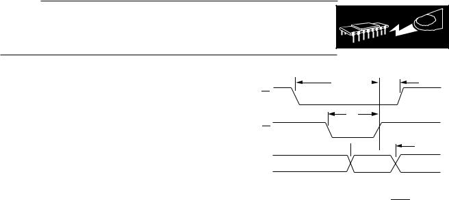
tCS |
30 |
ns min |
Chip Select to Write Setup Time |
tCH |
0 |
ns min |
Chip Select to Write Hold Time |
tWR |
30 |
ns min |
Write Pulsewidth |
tDS |
80 |
ns min |
Data Setup Time |
tDH |
0 |
ns min |
Data Hold Time |
NOTES
1Guaranteed by design and characterization, not production tested. Specifications subject to change without notice.
ABSOLUTE MAXIMUM RATINGS1
(TA = +25°C unless otherwise stated)
VDD to DGND . . . . . . . . . . . . . . |
. . . . . . . . . .–0.3 V to +17 V |
VSS to DGND . . . . . . . . . . . . . . |
. . . . . . . . . .+0.3 V to –17 V |
VREF to AGND . . . . . . . . . . . . . |
. . . VDD + 0.3 V, VSS – 0.3 V |
VRFB to AGND . . . . . . . . . . . . . |
. . . VDD + 0.3 V, VSS – 0.3 V |
VRA to AGND . . . . . . . . . . . . . . |
. . . VDD + 0.3 V, VSS – 0.3 V |
VRB to AGND . . . . . . . . . . . . . . |
. . . VDD + 0.3 V, VSS – 0.3 V |
VRC to AGND . . . . . . . . . . . . . . |
. . . VDD + 0.3 V, VSS – 0.3 V |
VOUT to AGND2 . . . . . . . . . . . . |
. . . VDD + 0.3 V, VSS – 0.3 V |
AGND to DGND . . . . . . . . . . . |
. . . . . . . . . . . . . –0.3 V, VDD |
Digital Input Voltage to DGND |
. . . . . –0.3 V to VDD + 0.3 V |
Power Dissipation (Any Package) |
|
To +75°C . . . . . . . . . . . . . . . |
. . . . . . . . . . . . . . . 650 mW |
Derates above +75°C . . . . . . . |
. . . . . . . . . . . . . . 10 mW/°C |
CAUTION |
|
Operating Temperature Range |
0°C to +70°C |
Commercial (J, K Versions) . . . . . . . . . . . |
|
Industrial (A, B Versions) . . . . . . . . . . . . |
–40°C to +85°C |
Extended (S, T Versions) . . . . . . . . . . . . |
–55°C to +125°C |
Storage Temperature Range . . . . . . . . . . . |
–65°C to +150°C |
Lead Temperature (Soldering, 10 sec) . . . . |
. . . . . . . +300°C |
NOTES
1Stresses above those listed under Absolute Maximum Ratings may cause permanent damage to the device. This is a stress rating only; functional operation of the device at these or any other conditions above those indicated in the operational sections of this specification is not implied. Exposure to absolute maximum rating conditions for extended periods of time may affect device reliability. Only one Absolute Maximum Rating may be applied at any one time. 2VOUT may be shorted to AGND provided that the power dissipation of the package is not exceeded.
ESD (electrostatic discharge) sensitive device. Electrostatic charges as high as 4000 V readily accumulate on the human body and test equipment and can discharge without detection. Although the AD7845 features proprietary ESD protection circuitry, permanent damage may occur on devices subjected to high energy electrostatic discharges. Therefore, proper ESD precautions are recommended to avoid performance degradation or loss of functionality.
WARNING! |
ESD SENSITIVE DEVICE |
ORDERING GUIDE1
|
|
Relative |
|
|
Temperature |
Accuracy |
Package |
Model2 |
Range |
@ +258C |
Option3 |
AD7845JN |
0°C to +70°C |
±1 LSB |
N-24 |
AD7845KN |
0°C to +70°C |
±1/2 LSB |
N-24 |
AD7845JP |
0°C to +70°C |
±1 LSB |
P-28A |
AD7845KP |
0°C to +70°C |
±1/2 LSB |
P-28A |
AD7845JR |
0°C to +70°C |
±1 LSB |
R-24 |
AD7845KR |
0°C to +70°C |
±1/2 LSB |
R-24 |
AD7845AQ |
–40°C to +85°C |
±1 LSB |
Q-24 |
AD7845BQ |
–40°C to +85°C |
±1/2 LSB |
Q-24 |
AD7845AR |
–40°C to +85°C |
±1 LSB |
R-24 |
AD7845BR |
–40°C to +85°C |
±1/2 LSB |
R-24 |
AD7845SQ/883B |
–55°C to +125°C |
±1 LSB |
Q-24 |
AD7845TQ/883B |
–55°C to +125°C |
±1/2 LSB |
Q-24 |
AD7845SE/883B |
–55°C to +125°C |
±1 LSB |
E-28A |
NOTES
1Analog Devices reserves the right to ship either ceramic (D-24A) or cerdip (Q-24) hermetic packages.
2To order MIL-STD-883, Class B processed parts, add /883B to part number. 3E = Leadless Ceramic Chip Carrier; N = Plastic DIP; P = Plastic Leaded Chip Carrier; Q = Cerdip; R = SOIC.
tCS |
|
tCH |
|
5V
CS
0V
tWR
5V
WR
0V
 tDS
tDS  tDH
tDH
5V
DATA
0V
NOTES
1. ALL INPUT SIGNAL RISE AND FALL TIMES MEASURED FROM 10% TO 90% OF +5V. tR = tF = 20ns.
2. TIMING MEASUREMENT REFERENCE LEVEL IS
Figure 1. AD7845 Timing Diagram
REV. B |
–3– |
AD7845
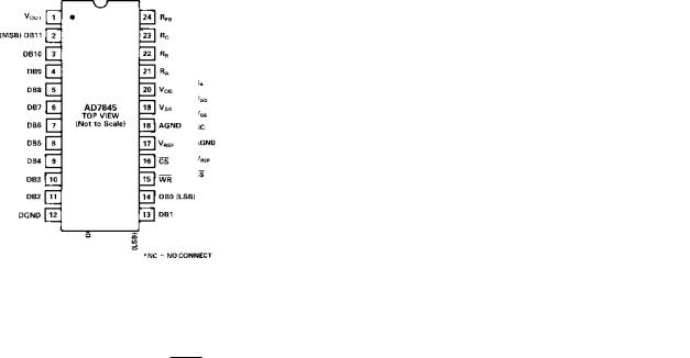
PIN CONFIGURATIONS
DIP, SOIC |
LCC |
PLCC |
TERMINOLOGY
LEAST SIGNIFICANT BIT
This is the analog weighting of 1 bit of the digital word in a
DAC. For the AD7845, 1 LSB = VREF12 .
2
RELATIVE ACCURACY
Relative accuracy or endpoint nonlinearity is a measure of the maximum deviation from a straight line passing through the endpoints of the DAC transfer function. It is measured after adjusting for both endpoints (i.e., offset and gain error are adjusted out) and is normally expressed in least significant bits or as a percentage of full-scale range.
DIFFERENTIAL NONLINEARITY
Differential nonlinearity is the difference between the measured change and the ideal 1 LSB change between any two adjacent codes. A specified differential nonlinearity of +1 LSB max over the operating temperature range ensures monotonicity.
GAIN ERROR
Gain error is a measure of the output error between an ideal DAC and the actual device output with all 1s loaded after offset error has been adjusted out. Gain error is adjustable to zero with an external potentiometer. See Figure 13.
ZERO CODE OFFSET ERROR
This is the error present at the device output with all 0s loaded in the DAC. It is due to the op amp input offset voltage and bias current and the DAC leakage current.
TOTAL HARMONIC DISTORTION
This is the ratio of the root-mean-square (rms) sum of the harmonics to the fundamental, expressed in dBs.
OUTPUT NOISE
This is the noise due to the white noise of the DAC and the input noise of the amplifier.
DIGITAL-TO-ANALOG GLITCH IMPULSE
This is the amount of charge injected from the digital inputs to the analog output when the inputs change state. This is normally specified as the area of the glitch in either pA-secs or nV-secs depending upon whether the glitch is measured as a current or voltage. The measurement takes place with VREF = AGND.
DIGITAL FEEDTHROUGH
When the DAC is not selected (i.e., CS is high) high frequency logic activity on the device digital inputs is capacitively coupled through the device to show up as noise on the VOUT pin. This noise is digital feedthrough.
MULTIPLYING FEEDTHROUGH ERROR
This is ac error due to capacitive feedthrough from the VREF terminal to VOUT when the DAC is loaded with all 0s.
OPEN-LOOP GAIN
Open-loop gain is defined as the ratio of a change of output
voltage to the voltage applied at the VREF pin with all 1s loaded in the DAC. It is specified at dc.
UNITY GAIN SMALL SIGNAL BANDWIDTH
This is the frequency at which the magnitude of the small signal voltage gain of the output amplifier is 3 dB below unity. The device is operated as a closed-loop unity gain inverter (i.e., DAC is loaded with all 1s).
OUTPUT RESISTANCE
This is the effective output source resistance.
FULL POWER BANDWIDTH
Full power bandwidth is specified as the maximum frequency, at unity closed-loop gain, for which a sinusoidal input signal will produce full output at rated load without exceeding a distortion level of 3%.
–4– |
REV. B |
 Loading...