


 Loading...
Analog Devices AD844SQ-883B, AD844SQ, AD844SCHIPS, AD844JR-16-REEL7, AD844JR-16-REEL Datasheet
...a |
60 MHz, 2000 V/ s |
|
Monolithic Op Amp |
||
|
|
|
|
|
AD844 |
|
|
|
FEATURES
Wide Bandwidth: 60 MHz at Gain of –1 Wide Bandwidth: 33 MHz at Gain of –10
Very High Output Slew Rate: Up to 2000 V/ s
20 MHz Full Power Bandwidth, 20 V p-p, RL = 500
Fast Settling: 100 ns to 0.1% (10 V Step) Differential Gain Error: 0.03% at 4.4 MHz Differential Phase Error: 0.158 at 4.4 MHz High Output Drive: 650 mA into 50 Load
Low Offset Voltage: 150 mV Max (B Grade) Low Quiescent Current: 6.5 mA
Available in Tape and Reel in Accordance with EIA-481A Standard
APPLICATIONS
Flash ADC Input Amplifiers
High-Speed Current DAC Interfaces
Video Buffers and Cable Drivers
Pulse Amplifiers
CONNECTION DIAGRAMS
8-Lead Plastic (N), |
16-Lead SOIC |
and Cerdip (Q) Packages |
(R) Package |
NULL |
1 |
AD844 |
–IN |
2 |
|
+IN |
3 |
|
–VS |
4 |
TOP VIEW |
(Not to Scale) |
8 |
NC |
1 |
AD844 |
16 |
NC |
NULL |
|
|
|
|
|
|
OFFSETNULL |
2 |
|
15 |
OFFSETNULL |
7 |
+VS |
|
|
|
V+ |
|
–IN |
3 |
|
14 |
|
6 |
OUTPUT |
|
|
|
|
|
NC |
4 |
|
13 |
NC |
5 |
TZ |
|
|
|
|
|
+IN |
5 |
|
12 |
OUTPUT |
|
NC |
6 |
|
11 |
TZ |
|
V– |
7 |
|
10 |
NC |
|
NC |
8 |
TOP VIEW |
9 |
NC |
|
(Not to Scale) |
NC = NO CONNECT
PRODUCT DESCRIPTION
The AD844 is a high-speed monolithic operational amplifier fabricated using Analog Devices’ junction isolated complementary bipolar (CB) process. It combines high bandwidth and very fast large signal response with excellent dc performance. Although optimized for use in current to voltage applications and as an inverting mode amplifier, it is also suitable for use in many noninverting applications.
The AD844 can be used in place of traditional op amps, but its current feedback architecture results in much better ac performance, high linearity and an exceptionally clean pulse response.
This type of op amp provides a closed-loop bandwidth which is determined primarily by the feedback resistor and is almost independent of the closed-loop gain. The AD844 is free from the slew rate limitations inherent in traditional op amps and other current-feedback op amps. Peak output rate of change can be over 2000 V/µs for a full 20 V output step. Settling time is typically 100 ns to 0.1%, and essentially independent of gain. The AD844 can drive 50 Ω loads to ±2.5 V with low distortion and is short circuit protected to 80 mA.
The AD844 is available in four performance grades and three package options. In the 16-lead SOIC (R) package, the AD844J is specified for the commercial temperature range of 0°C to 70°C. The AD844A and AD844B are specified for the industrial temperature range of –40°C to +85°C and are available in the cerdip (Q)
REV. D
Information furnished by Analog Devices is believed to be accurate and reliable. However, no responsibility is assumed by Analog Devices for its use, nor for any infringements of patents or other rights of third parties that may result from its use. No license is granted by implication or otherwise under any patent or patent rights of Analog Devices.
package. The AD844A is also available in an 8-lead plastic mini-DIP (N). The AD844S is specified over the military temperature range of –55°C to +125°C. It is available in the 8-lead cerdip (Q) package. “A” and “S” grade chips and devices processed to MIL-STD-883B, REV. C are also available.
PRODUCT HIGHLIGHTS
1.The AD844 is a versatile, low cost component providing an excellent combination of ac and dc performance.
2.It is essentially free from slew rate limitations. Rise and fall times are essentially independent of output level.
3.The AD844 can be operated from ± 4.5 V to ± 18 V power supplies and is capable of driving loads down to 50 Ω, as well as driving very large capacitive loads using an external network.
4.The offset voltage and input bias currents of the AD844 are
laser trimmed to minimize dc errors; VOS drift is typically 1 µV/°C and bias current drift is typically 9 nA/°C.
5.The AD844 exhibits excellent differential gain and differential phase characteristics, making it suitable for a variety of video applications with bandwidths up to 60 MHz.
6.The AD844 combines low distortion, low noise and low drift with wide bandwidth, making it outstanding as an input amplifier for flash A/D converters.
One Technology Way, P.O. Box 9106, Norwood, MA 02062-9106, U.S.A.
Tel: 781/329-4700 |
www.analog.com |
Fax: 781/326-8703 |
© Analog Devices, Inc., 2001 |

AD844–SPECIFICATIONS (@ TA = 25 C and VS = 15 V dc, unless otherwise noted)
|
|
|
AD844J/A |
|
|
AD844B |
|
AD844S |
|
|
|
Model |
Conditions |
Min |
Typ |
Max |
Min |
Typ |
Max |
Min |
Typ |
Max |
Unit |
INPUT OFFSET VOLTAGE1 |
|
|
50 |
300 |
|
50 |
150 |
|
50 |
300 |
µV |
TMIN–TMAX |
|
|
75 |
500 |
|
75 |
200 |
|
125 |
500 |
µV |
vs. Temperature |
|
|
1 |
|
|
1 |
5 |
|
1 |
5 |
µV/°C |
vs. Supply |
5 V–18 V |
|
|
|
|
|
|
|
|
|
µV/V |
Initial |
|
|
4 |
20 |
|
4 |
10 |
|
4 |
20 |
|
TMIN–TMAX |
VCM = ± 10 V |
|
4 |
|
|
4 |
10 |
|
4 |
20 |
µV/V |
vs. Common Mode |
|
|
|
|
|
|
|
|
|
µV/V |
|
Initial |
|
|
10 |
35 |
|
10 |
20 |
|
10 |
35 |
|
TMIN–TMAX |
|
|
10 |
|
|
10 |
20 |
|
10 |
35 |
µV/V |
INPUT BIAS CURRENT |
|
|
|
|
|
|
|
|
|
|
|
–Input Bias Current1 |
|
|
200 |
450 |
|
150 |
250 |
|
200 |
450 |
nA |
TMIN–TMAX |
|
|
800 |
1500 |
|
750 |
1100 |
|
1900 |
2500 |
nA |
vs. Temperature |
|
|
9 |
|
|
9 |
15 |
|
20 |
30 |
nA/°C |
vs. Supply |
5 V–18 V |
|
|
|
|
|
|
|
|
|
|
Initial |
|
|
175 |
250 |
|
175 |
200 |
|
175 |
250 |
nA/V |
TMIN–TMAX |
VCM = ± 10 V |
|
220 |
|
|
220 |
240 |
|
220 |
300 |
nA/V |
vs. Common Mode |
|
|
|
|
|
|
|
|
|
|
|
Initial |
|
|
90 |
160 |
|
90 |
110 |
|
90 |
160 |
nA/V |
TMIN–TMAX |
|
|
110 |
|
|
110 |
150 |
|
120 |
200 |
nA/V |
+Input Bias Current1 |
|
|
150 |
400 |
|
100 |
200 |
|
100 |
400 |
nA |
TMIN–TMAX |
|
|
350 |
700 |
|
300 |
500 |
|
800 |
1300 |
nA |
vs. Temperature |
|
|
3 |
|
|
3 |
7 |
|
7 |
15 |
nA/°C |
vs. Supply |
5 V–18 V |
|
|
|
|
|
|
|
|
|
|
Initial |
|
|
80 |
150 |
|
80 |
100 |
|
80 |
150 |
nA/V |
TMIN–TMAX |
VCM = ± 10 V |
|
100 |
|
|
100 |
120 |
|
120 |
200 |
nA/V |
vs. Common Mode |
|
|
|
|
|
|
|
|
|
|
|
Initial |
|
|
90 |
150 |
|
90 |
120 |
|
90 |
150 |
nA/V |
TMIN–TMAX |
|
|
130 |
|
|
130 |
190 |
|
140 |
200 |
nA/V |
INPUT CHARACTERISTICS |
|
|
|
|
|
|
|
|
|
|
|
Input Resistance |
|
|
|
|
|
|
|
|
|
|
Ω |
–Input |
|
|
50 |
65 |
|
50 |
65 |
|
50 |
65 |
|
+Input |
|
7 |
10 |
|
7 |
10 |
|
7 |
10 |
|
MΩ |
Input Capacitance |
|
|
|
|
|
|
|
|
|
|
|
–Input |
|
|
2 |
|
|
2 |
|
|
2 |
|
pF |
+Input |
|
|
2 |
|
|
2 |
|
|
2 |
|
pF |
Input Voltage Range |
|
± 10 |
|
|
± 10 |
|
|
± 10 |
|
|
|
Common Mode |
|
|
|
|
|
|
|
V |
|||
|
|
|
|
|
|
|
|
|
|
|
|
INPUT VOLTAGE NOISE |
f ≥ 1 kHz |
|
2 |
|
|
2 |
|
|
2 |
|
nV/√Hz |
|
|
|
|
|
|
|
|
|
|
|
|
INPUT CURRENT NOISE |
f ≥ 1 kHz |
|
|
|
|
|
|
|
|
|
pA/√Hz |
–Input |
|
10 |
|
|
10 |
|
|
10 |
|
||
+Input |
f ≥ 1 kHz |
|
12 |
|
|
12 |
|
|
12 |
|
pA/√Hz |
|
|
|
|
|
|
|
|
|
|
|
|
OPEN LOOP TRANSRESISTANCE |
VOUT = ± 10 V |
|
|
|
|
|
|
|
|
|
|
|
RLOAD = 500 Ω |
2.2 |
3.0 |
|
2.8 |
3.0 |
|
2.2 |
3.0 |
|
MΩ |
TMIN–TMAX |
|
1.3 |
2.0 |
|
1.6 |
2.0 |
|
1.3 |
1.6 |
|
MΩ |
Transcapacitance |
|
|
4.5 |
|
|
4.5 |
|
|
4.5 |
|
pF |
|
|
|
|
|
|
|
|
|
|
|
|
DIFFERENTIAL GAIN ERROR2 |
f = 4.4 MHz |
|
0.03 |
|
|
0.03 |
|
|
0.03 |
|
% |
DIFFERENTIAL PHASE ERROR2 |
f = 4.4 MHz |
|
0.15 |
|
|
0.15 |
|
|
0.15 |
|
Degree |
FREQUENCY RESPONSE |
|
|
|
|
|
|
|
|
|
|
|
Small Signal Bandwidth |
|
|
|
|
|
|
|
|
|
|
|
Gain = –13 |
|
|
60 |
|
|
60 |
|
|
60 |
|
MHz |
Gain = –104 |
|
|
33 |
|
|
33 |
|
|
33 |
|
MHz |
TOTAL HARMOMIC DISTORTION |
f = 100 kHz, |
|
|
|
|
|
|
|
|
|
|
|
2 V rms5 |
|
0.005 |
|
|
0.005 |
|
|
0.005 |
|
% |
SETTLING TIME |
± 15 V Supplies |
|
|
|
|
|
|
|
|
|
|
10 V Output Step |
|
|
|
|
|
|
|
|
|
|
|
Gain = –1, to 0.1%5 |
|
|
100 |
|
|
100 |
|
|
100 |
|
ns |
Gain = –10, to 0.1%6 |
± 5 V Supplies |
|
100 |
|
|
100 |
|
|
100 |
|
ns |
2 V Output Step |
|
|
|
|
|
|
|
|
|
|
|
Gain = –1, to 0.1%5 |
|
|
110 |
|
|
110 |
|
|
110 |
|
ns |
Gain = –10, to 0.1%6 |
|
|
100 |
|
|
100 |
|
|
100 |
|
ns |
–2– |
REV. D |
|
|
|
|
|
|
|
|
|
|
|
AD844 |
|
|
|
|
|
|
|
|
|
|
|
|
|
|
|
|
AD844J/A |
|
|
AD844B |
|
|
AD844S |
|
|
|
|
Model |
Conditions |
Min |
Typ |
Max |
Min |
Typ |
Max |
Min |
Typ |
Max |
|
Unit |
OUTPUT SLEW RATE |
Overdriven |
|
|
|
|
|
|
|
|
|
|
V/µs |
|
Input |
1200 |
2000 |
|
1200 |
2000 |
|
1200 |
2000 |
|
|
|
|
|
|
|
|
|
|
|
|
|
|
|
|
FULL POWER BANDWIDTH |
VS = ± 15 V |
|
|
|
|
|
|
|
|
|
|
|
VOUT = 20 V p-p5 |
|
20 |
|
|
20 |
|
|
20 |
|
|
MHz |
|
VOUT = 2 V p-p5 |
VS = ± 5 V |
|
20 |
|
|
20 |
|
|
20 |
|
|
MHz |
|
THD = 3% |
|
|
|
|
|
|
|
|
|
|
|
|
|
|
|
|
|
|
|
|
|
|
|
|
OUTPUT CHARACTERISTICS |
RLOAD = 500 Ω |
|
|
|
|
|
|
|
|
|
|
± V |
Voltage |
10 |
11 |
|
10 |
11 |
|
10 |
11 |
|
|
||
Short Circuit Current |
|
|
80 |
|
|
80 |
|
|
80 |
|
|
mA |
TMIN–TMAX |
|
|
60 |
|
|
60 |
|
|
60 |
|
|
mA |
Output Resistance |
Open Loop |
|
15 |
|
|
15 |
|
|
15 |
|
|
Ω |
|
|
|
|
|
|
|
|
|
|
|
|
|
POWER SUPPLY |
|
|
|
|
|
|
|
|
|
|
|
|
Operating Range |
|
± 4.5 |
|
± 18 |
± 4.5 |
|
± 18 |
+4.5 |
|
± 18 |
|
V |
Quiescent Current |
|
|
6.5 |
7.5 |
|
6.5 |
7.5 |
|
6.5 |
7.5 |
|
mA |
TMIN–TMAX |
|
|
7.5 |
8.5 |
|
7.5 |
8.5 |
|
8.5 |
9.5 |
|
mA |
NOTES
1Rated performance after a 5 minute warmup at TA = 25°C.
2Input signal 285 mV p-p carrier (40 IRE) riding on 0 mV to 642 mV (90 IRE) ramp. R L= 100 Ω; R1, R2 = 300 Ω. 3Input signal 0 dBm, CL = 10 pF, RL = 500 Ω, R1 = 500 Ω, R2 = 500 Ω in Figure 2.
4Input signal 0 dBm, CL =10 pF, RL = 500 Ω, R1 = 500 Ω, R2 = 50 Ω in Figure 2. 5CL = 10 pF, RL = 500 Ω, R1 = 1 kΩ, R2 = 1 kΩ in Figure 2.
6CL = 10 pF, RL = 500 Ω, R1 = 500 Ω, R2 = 50 Ω in Figure 2.
Specifications subject to change without notice. All min and max specifications are guaranteed.
ABSOLUTE MAXIMUM RATINGS1 |
± 18 V |
Supply Voltage . . . . . . . . . . . . . . . . . . . . . . . . |
|
Power Dissipation2 . . . . . . . . . . . . . . . . . . . . |
. . . . . . . . 1.1 W |
Output Short Circuit Duration . . . . . . . . . . . |
. . . . . . Indefinite |
Common-Mode Input Voltage . . . . . . . . . . . |
. . . . . . . . . . ± VS |
Differential Input Voltage . . . . . . . . . . . . . . . |
. . . . . . . . . . 6 V |
Inverting Input Current |
|
Continuous . . . . . . . . . . . . . . . . . . . . . . . . |
. . . . . . . . . 5 mA |
Transient . . . . . . . . . . . . . . . . . . . . . . . . . . |
. . . . . . . . 10 mA |
Storage Temperature Range (Q) . . . . . . . . . |
–65°C to +150°C |
(N, R) . . . . . . . |
–65°C to +125°C |
Lead Temperature Range (Soldering 60 sec) . |
. . . . . . . . 300°C |
ESD Rating . . . . . . . . . . . . . . . . . . . . . . . . . . |
. . . . . . . 1000 V |
ORDERING GUIDE
|
Temperature |
Package |
Model |
Range |
Option* |
|
|
|
AD844AN |
–40°C to +85°C |
N-8 |
AD844ACHIPS |
–40°C to +85°C |
Die |
AD844AQ |
–40°C to +85°C |
Q-8 |
AD844BQ |
–40°C to +85°C |
Q-8 |
AD844JR-16 |
0°C to 70°C |
R-16 |
AD844JR-16-REEL |
0°C to 70°C |
13" Tape |
|
0°C to 70°C |
and Reel |
AD844JR-16-REEL7 |
7" Tape |
|
|
–55°C to +125°C |
and Reel |
AD844SCHIPS |
Die |
|
AD844SQ |
–55°C to +125°C |
Q-8 |
AD844SQ/883B |
–55°C to +125°C |
Q-8 |
5962-8964401PA |
–55°C to +125°C |
Q-8 |
*N = Plastic DIP; Q = Cerdip; R = Small Outline IC (SOIC).
NOTES
1Stresses above those listed under Absolute Maximum Ratings may cause permanent damage to the device at these or any other conditions above those indicated in the operational sections of this specification is not implied. Exposure to absolute maximum rating conditions for extended periods may affect device reliability.
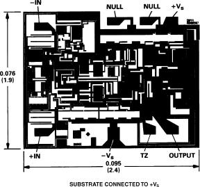
28-Lead Plastic Package:
8-Lead Cerdip Package:
16-Lead SOIC Package:
METALIZATION PHOTOGRAPH
Contact factory for latest dimensions.
Dimension shown in inches and (mm).
REV. D |
–3– |
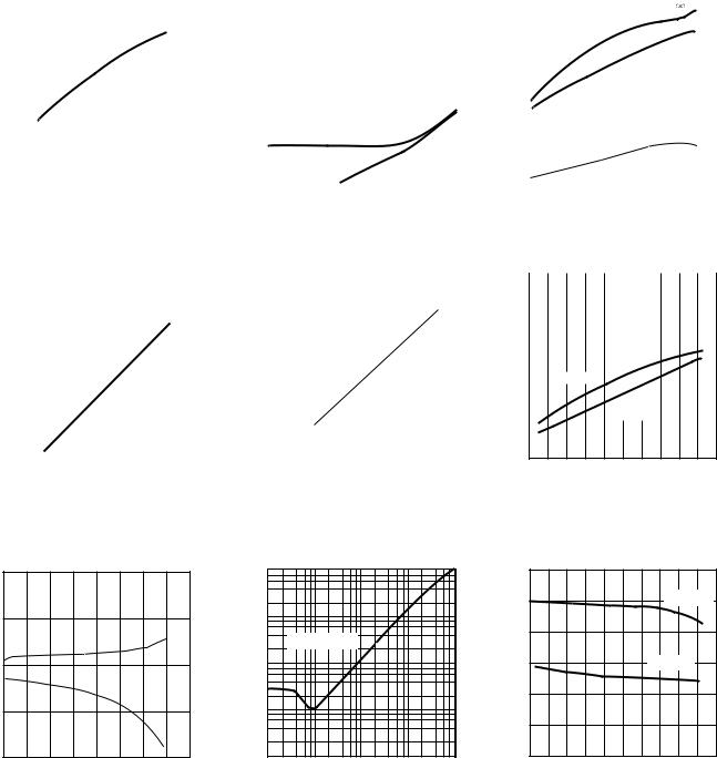
AD844–Typical Characteristics (TA = 25 C and VS = 15 V, unless otherwise noted)
MHz– |
70 |
|
|
|
|
|
|
|
|
|
60 |
|
|
|
|
|
|
|
|
|
|
BANDWIDTH3dB– |
|
|
|
|
|
|
|
|
|
|
40 |
|
|
|
|
|
|
|
|
|
|
|
50 |
|
|
|
|
|
|
|
|
|
|
30 |
|
|
|
|
|
|
|
|
|
|
|
|
|
|
|
|
|
|
|
|
|
5 |
10 |
15 |
|
20 |
|||||
|
0 |
|
||||||||
|
|
|
SUPPLY VOLTAGE – V |
|
|
|||||
|
TPC 1. –3 dB Bandwidth vs. |
|
|
|||||||
|
Supply Voltage R1 = R2 = 500 Ω |
|||||||||
– V |
20 |
|
|
|
|
|
|
|
|
|
|
TA = 25 C |
|
|
|
|
|
|
|
||
|
|
|
|
|
|
|
|
|
||
VOLTAGEOUTPUT |
15 |
|
|
|
|
|
|
|
|
|
|
|
|
|
|
|
|
|
|
|
|
OF THE |
10 |
|
|
|
|
|
|
|
|
|
|
|
|
|
|
|
|
|
|
||
|
|
|
|
|
|
|
|
|
|
|
|
|
|
|
|
|
|
|
|
|
|
MAGNITUDE |
5 |
|
|
|
|
|
|
|
|
|
|
|
|
|
|
|
|
|
|
||
|
|
|
|
|
|
|
|
|
|
|
|
0 |
|
|
|
|
|
|
|
|
|
|
|
5 |
10 |
15 |
|
20 |
||||
|
0 |
|
||||||||
SUPPLY VOLTAGE – V
TPC 4. Noninverting Input Voltage Swing vs. Supply Voltage
|
|
–60 |
|
|
|
|
|
|
|
|
|
|
|
|
|
|
|
|
|
|
|
|
|
|
|
|
|
|
|
|
|
|
|
|
|
|
|
|
|
|
|
|
|
|
|
|
|
|
|
|
|
|
|
|
|
||
– dB |
|
–70 |
|
|
|
|
|
|
|
|
|
|
|
|
|
|
|
|
|
|
|
|
|
|
|
|
|
|
|
|
|
|
|
|
|
|
|
|
|
|
|
|
|
|
|
|
|
|
|
|
|
|
|
|
|||
|
–80 |
|
|
|
|
|
|
|
|
|
|
|
|
|
|
|
|
|
|
|
|
|
|
|
|
|
||
DISTORTION |
|
|
|
|
|
|
|
|
|
|
|
|
|
|
|
|
|
|
|
|
|
|
|
|
|
|
||
|
|
|
|
|
|
|
|
|
|
|
|
|
|
|
|
|
|
|
|
|
|
|
|
|
|
|||
|
|
|
|
|
|
|
1V rms |
|
|
|
|
|
|
|
|
|
|
|
|
|
|
|
|
|
||||
|
|
–90 |
|
|
|
|
|
|
|
|
|
|
|
|
|
|
|
|
|
|
|
|
|
|
|
|
|
|
|
|
|
|
|
|
|
|
|
|
|
|
|
|
|
|
|
|
|
|
|
|
|
|
|
|
|
||
HARMONIC |
–100 |
|
|
|
|
|
|
|
|
|
|
|
|
|
|
|
|
|
|
|
|
|
|
|
|
|
||
|
|
|
|
|
|
|
|
|
|
|
|
|
|
|
|
|
|
|
|
|
|
|
|
|
||||
–110 |
|
|
|
|
|
|
|
|
|
|
|
|
|
|
|
|
|
|
|
|
|
|
|
|
|
|||
|
|
|
|
|
2ND HARMONIC |
|
|
|
|
|
|
|
|
|
|
|
|
|
||||||||||
|
|
|
|
|
|
|
|
|
|
|
|
|
|
|
|
|
|
|
|
|
||||||||
|
–120 |
|
|
|
|
|
|
|
|
|
|
|
|
|
|
|
|
|
|
|
|
|
|
|
|
|
||
|
|
|
|
|
|
|
|
|
|
|
|
|
|
|
|
|
|
|
|
|
|
|
|
|
|
|||
|
|
|
|
|
|
|
|
|
|
|
|
|
|
|
|
|
|
|
|
|
|
|
|
|
|
|
|
|
|
–130 |
|
|
|
|
|
|
|
|
|
|
|
|
|
|
|
3RD HARMONIC |
|
|
|||||||||
|
|
|
|
|
|
|
|
|
|
|
|
|
|
|
|
|
|
|
|
|
|
|
|
|
|
|||
|
|
|
|
|
|
|
|
|
|
|
|
|
|
|
|
10k |
|
|
|
|
|
|||||||
|
|
100 |
|
|
|
|
|
|
1k |
|
|
|
100k |
|||||||||||||||
|
|
|
|
|
|
|
|
|
INPUT FREQUENCY – Hz |
|
|
|
|
|
||||||||||||||
|
|
TPC 2. Harmonic Distortion vs. |
||||||||||||||||||||||||||
|
|
Frequency, R1 = R2 = 1 kΩ |
|
|
|
|
|
|||||||||||||||||||||
|
– V |
20 |
|
|
|
|
|
|
|
|
|
|
|
|
|
|
|
|
|
|
|
|
|
|
|
|
|
|
|
|
|
|
|
RL = 500 |
|
|
|
|
|
|
|
|
|
|
|
|
|
|
|
|
|
||||||
|
VOLTAGEOUTPUT |
|
|
|
|
|
|
|
|
|
|
|
|
|
|
|
|
|
|
|
|
|
||||||
|
|
|
|
|
TA |
= 25 C |
|
|
|
|
|
|
|
|
|
|
|
|
|
|
|
|
|
|||||
|
|
15 |
|
|
|
|
|
|
|
|
|
|
|
|
|
|
|
|
|
|
|
|
|
|
|
|
|
|
|
|
|
|
|
|
|
|
|
|
|
|
|
|
|
|
|
|
|
|
|
|
|
|
|
|
|
|
|
|
OF THE |
10 |
|
|
|
|
|
|
|
|
|
|
|
|
|
|
|
|
|
|
|
|
|
|
|
|
|
|
|
|
|
|
|
|
|
|
|
|
|
|
|
|
|
|
|
|
|
|
|
|
|
|
|
|
|
||
|
|
|
|
|
|
|
|
|
|
|
|
|
|
|
|
|
|
|
|
|
|
|
|
|
|
|
|
|
|
MAGNITUDE |
5 |
|
|
|
|
|
|
|
|
|
|
|
|
|
|
|
|
|
|
|
|
|
|
|
|
|
|
|
|
|
|
|
|
|
|
|
|
|
|
|
|
|
|
|
|
|
|
|
|
|
|
|
|
|
|
|
|
|
0 |
|
|
|
|
|
|
|
|
|
|
|
|
|
|
|
|
|
|
|
|
|
|
|
|
|
|
|
|
|
|
|
|
5 |
|
10 |
15 |
20 |
||||||||||||||||||
|
|
0 |
|
|
|
|||||||||||||||||||||||
SUPPLY VOLTAGE – V
TPC 5. Output Voltage Swing vs. Supply Voltage
|
5 |
|
|
|
|
|
|
|
|
|
|
|
|
|
|
|
|
|
|
|
|
|
|
|
|
|
|
|
|
|
|
|
|
|
|
RL = |
|
|
|
|
|
|
|||||
|
|
|
|
|
|
|
|
|
|
|
|
|
|
|
|
|
|
|
|
||||
M |
4 |
|
|
|
|
|
|
|
|
|
|
|
|
|
|
|
|
|
|
|
|
|
|
|
|
|
|
|
|
|
|
|
|
|
|
|
|
|
|
|
|
|
|
|
|||
|
|
|
|
|
|
|
|
|
|
|
|
|
|
|
|
|
|
|
|
|
|
|
|
– |
|
|
|
|
|
|
|
|
|
|
|
|
|
|
|
RL = 500 |
|
|
|
|
|||
TRANSRESISTANCE |
3 |
|
|
|
|
|
|
|
|
|
|
|
|
|
|
|
|
|
|
|
|
|
|
|
|
|
|
|
|
|
|
|
|
|
|
|
|
|
|
|
|
|
|
|
|
||
|
|
|
|
|
|
|
|
|
|
|
|
|
|
|
|
|
|
|
|
|
|
|
|
|
2 |
|
|
|
|
|
|
|
|
|
|
|
|
|
|
|
|
|
|
|
|
|
|
|
|
|
|
|
|
|
|
|
|
|
|
|
|
|
|
|
|
|
|
|
|
||
|
|
|
|
|
|
|
|
|
|
|
|
|
|
|
|
|
|
|
|
|
|
|
|
|
|
|
|
|
|
|
|
|
|
|
|
|
|
|
|
RL = 50 |
|
|
|
|
|||
|
1 |
|
|
|
|
|
|
|
|
|
|
|
|
|
|
|
|
|
|
|
|
|
|
|
|
|
|
|
|
|
|
|
|
|
|
|
|
|
|
|
|
|
|
|
|
||
|
0 |
|
|
|
|
|
|
|
|
|
|
|
|
|
|
|
|
|
|
|
|
|
|
|
|
0 |
|
|
|
50 |
|
|
100 |
|
|
150 |
|||||||||||
|
–50 |
|
|
|
|
|
|
|
|||||||||||||||
|
|
|
|
|
|
TEMPERATURE – C |
|
|
|
|
|||||||||||||
|
TPC 3. Transresistance vs. |
|
|
|
|
||||||||||||||||||
|
Temperature |
|
|
|
|
|
|
|
|
|
|
|
|
|
|
||||||||
|
10 |
|
|
|
|
|
|
|
|
|
|
|
|
|
|
|
|
|
|
|
|
|
|
|
|
|
|
|
|
|
|
|
|
|
|
|
|
|
|
|
|
|
|
|
|
|
|
– mA |
9 |
|
|
|
|
|
|
|
|
|
|
|
|
|
|
|
|
|
|
|
|
|
|
|
|
|
|
|
|
|
|
|
|
|
|
|
|
|
|
|
|
|
|
|
|
||
8 |
|
|
|
|
|
|
|
|
|
|
|
|
|
|
|
|
|
|
|
|
|
|
|
CURRENT |
|
|
|
|
|
|
|
|
|
|
|
|
|
|
|
|
|
|
|
|
|
|
|
7 |
|
|
VS = 15V |
|
|
|
|
|
|
|
|
|
|
|
|
|
|
||||||
SUPPLY |
6 |
|
|
|
|
|
|
|
|
VS |
= |
5V |
|
|
|
|
|
|
|
|
|
|
|
|
|
|
|
|
|
|
|
|
|
|
|
|
|
|
|
|
|
||||||
|
|
|
|
|
|
|
|
|
|
|
|
|
|
|
|
|
|
|
|
|
|
|
|
|
5 |
|
|
|
|
|
|
|
|
|
|
|
|
|
|
|
|
|
|
|
|
|
|
|
|
|
|
|
|
|
|
|
|
|
|
|
|
|
|
|
|
|
|
|
|
|
|
|
|
|
|
|
|
|
|
|
|
|
|
|
|
|
|
|
|
|
|
|
|
|
|
4
–60 –40 –20 0 20 40 60 80 100 120 140 TEMPERATURE – C
TPC 6. Quiescent Supply Current vs. Temperature and Supply Voltage
|
2 |
|
|
|
|
|
100 |
|
|
|
|
A |
1 |
|
|
|
|
|
10 |
|
|
|
|
– |
|
|
|
|
– |
|
|
|
|
||
|
|
|
|
|
|
|
|
|
|
||
CURRENTBIASINPUT |
|
|
|
IBN |
|
IMPEDANCEOUTPUT |
|
5V SUPPLIES |
|
|
|
|
|
|
|
|
|
|
|
|
|
||
|
0 |
|
|
IBP |
|
|
1 |
|
|
|
|
|
|
|
|
|
|
|
|
|
|
||
|
–1 |
|
|
|
|
|
0.1 |
|
|
|
|
|
–2 |
|
|
|
|
|
0.01 |
|
1M |
10M |
|
|
0 |
50 |
100 |
|
|
10k |
100k |
100M |
|||
|
–50 |
150 |
|
||||||||
|
|
|
TEMPERATURE – C |
|
|
|
|
FREQUENCY – Hz |
|
||
TPC 7. Inverting Input Bias Cur- |
TPC 8. Output Impedance vs. |
rent (IBN) and Noninverting Input |
Frequency, Gain = –1, R1 = R2 = 1 kΩ |
Bias Current (IBP) vs. Temperature |
|
|
40 |
|
|
|
|
|
|
|
35 |
|
|
|
|
VS = 15V |
|
– MHz |
30 |
|
|
|
|
|
|
BANDWIDTH |
25 |
|
|
|
VS = 5V |
|
|
20 |
|
|
|
|
|
|
|
–3dB |
|
|
|
|
|
|
|
|
|
|
|
|
|
|
|
|
15 |
|
|
|
|
|
|
|
10 |
|
|
|
|
|
|
|
–60 –40 –20 |
0 |
20 40 |
60 |
80 |
100 120 |
140 |
|
|
TEMPERATURE – C |
|
|
|||
TPC 9. –3 dB Bandwidth vs. Temperature, Gain = –1, R1 = R2 = 1 kΩ
–4– |
REV. 0 |

Inverting Gain-of-1 AC Characteristics |
|
|
||||||
|
|
+VS |
|
|
6 |
|
R1 = R2 = 500 |
|
|
|
4.7 |
|
|
|
|
||
|
0.22 F |
|
|
|
|
|
|
|
|
|
|
|
|
|
|
|
|
|
|
R1 |
|
|
0 |
|
|
|
|
|
|
|
|
|
|
|
|
|
|
|
|
dB |
–6 |
|
R1 = R2 = 1k |
|
|
R2 |
|
|
|
|
|
||
VIN |
|
|
– |
|
|
|
|
|
– |
|
|
|
|
|
|
||
|
|
GAIN |
|
|
|
|
||
|
AD844 |
VOUT |
–12 |
|
|
|
||
|
+ |
|
|
|
|
|
|
|
|
|
|
|
|
|
|
|
|
|
|
RL |
CL |
|
–18 |
|
|
|
|
0.22 F |
4.7 |
|
|
|
|
|
|
|
|
|
|
–24 |
|
|
|
|
|
–VS |
|
|
|
100k |
1M |
10M |
100M |
|
|
|
|
|
FREQUENCY – Hz |
|
||
|
|
|
|
|
|
|
||
TPC 10. Inverting Amplifier, |
TPC 11. Gain vs. Frequency for |
Gain of –1 (R1 = R2) |
Gain = –1, RL = 500 Ω, CL = 0 pF |
AD844
|
–180 |
|
|
|
|
|
|
|
|
|
|
|
|
|
Degrees– |
–210 |
|
|
|
|
|
|
|
|
|
|
|
|
|
|
|
|
|
|
|
|
|
|
|
|
|
|
||
|
|
|
|
|
|
|
|
|
|
|
|
|
||
|
|
|
|
|
|
|
|
|
|
|
|
|
|
|
–240 |
|
|
|
|
|
|
|
R1 = R2 = 500 |
|
|
||||
|
|
|
|
|
|
|
|
|
|
|||||
PHASE |
|
|
|
|
|
|
|
|
|
|
|
|
|
|
–270 |
|
|
|
|
|
|
|
|
|
|
|
|
|
|
|
|
|
|
|
|
|
|
|
|
|
|
|
||
|
|
|
|
|
|
|
|
|
|
|
|
|
|
|
|
|
|
|
R1 = R2 = 1k |
|
|
|
|
|
|
|
|||
|
–300 |
|
|
|
|
|
|
|
|
|
|
|
|
|
|
|
|
|
|
|
|
|
|
|
|
|
|
|
|
|
|
|
|
|
|
|
|
|
|
|
|
|
|
|
|
–330 |
|
|
|
|
|
|
|
|
|
|
|
|
|
|
|
|
|
|
|
|
|
|
|
|
|
|
|
|
|
|
|
|
|
|
|
|
|
|
|
|
|
|
|
|
0 |
25 |
|
|
|
|
|
50 |
||||||
|
|
|
|
FREQUENCY – MHz |
|
|
||||||||
TPC 12. Phase vs. Frequency Gain = –1, RL = 500 Ω, CL = 0 pF
TPC 13. Large Signal Pulse |
TPC 14. Small Signal Pulse |
Response, Gain = –1, R1 = R2 = 1 kΩ |
Response, Gain = –1, R1 = R2 = 1 kΩ |
|
|
Inverting Gain-of-10 AC Characteristics
|
|
|
|
26 |
|
|
|
|
|
+VS |
|
|
|
RL = 500 |
|
|
0.22 F |
4.7 |
|
20 |
|
|
|
|
|
|
|
|
|
|
|
|
|
500 |
dB– |
14 |
|
RL = 50 |
|
|
|
|
|
|
|
||
|
|
|
GAIN |
|
|
|
|
VIN |
– |
|
8 |
|
|
|
|
|
50 |
|
|
|
|
|
|
|
AD844 |
VOUT |
|
|
|
|
|
|
+ |
|
|
2 |
|
|
|
|
|
|
|
|
|
|
|
|
|
RL |
CL |
|
|
|
|
|
0.22 F |
|
|
–4 |
|
|
|
|
4.7 |
|
100k |
1M |
10M |
100M |
|
|
|
|
|
FREQUENCY – Hz |
|
||
|
|
|
|
|
|
||
|
–VS |
|
|
|
|
|
|
TPC 15. Gain of –10 Amplifier |
TPC 16. Gain vs. Frequency, |
|
|||||
|
|
|
|
Gain = –10 |
|
|
|
|
–180 |
|
|
|
|
|
|
|
|
|
|
|
|
|
Degrees |
–210 |
|
|
|
|
|
|
|
|
|
|
|
|
|
|
|
|
|
|
|
|
|
|
|
|
|
|
||
|
|
|
|
|
|
|
|
|
|
|
|
|
||
–240 |
|
|
|
|
|
|
|
|
|
|
|
|
|
|
|
|
|
|
|
|
|
RL |
= 500 |
|
|
|
|||
– |
|
|
|
|
|
|
|
|
|
|
|
|
|
|
PHASE |
–270 |
|
|
|
|
|
|
|
|
|
|
|
|
|
|
|
|
|
|
RL = 50 |
|
|
|
|
|
||||
|
|
|
|
|
|
|
|
|
|
|
||||
|
–300 |
|
|
|
|
|
|
|
|
|
|
|
|
|
|
|
|
|
|
|
|
|
|
|
|
|
|
|
|
|
–330 |
|
|
|
|
|
|
|
|
|
|
|
|
|
|
|
|
|
|
|
|
|
|
|
|
|
|
|
|
|
|
25 |
|
|
|
|
|
|
||||||
|
0 |
|
|
|
50 |
|||||||||
|
|
|
|
FREQUENCY – MHz |
|
|
|
|||||||
TPC 17. Phase vs. Frequency, Gain = –10
REV. D |
–5– |
Loading...