


ADAU1701
FEATURES
28/56-bit, 50 MHz digital audio processor
Stereo ADC: 102 dB dynamic range and -90 dB THD+N 4-channel DAC: 103 dB dynamic range and -90 dB THD+N Complete stand-alone operation
Self-boot from serial EEPROM
Auxiliary ADC with four-input mux for analog control GPIOs for digital controls and outputs
Fully programable with SigmaStudio’ gr aphical tool Sampling rates up to 192 kHz supported
28-bit × 28-bit multiplier with 56-bit accumulator Double precision mode for full 56-bit processing
Clock Oscillator for generating master clock from crystal
PLL for generating master clock from 64 × fS, 256 × fS, 384 × fS, or 512 × fS clocks
Flexible serial data I/O ports with I2S compatible, leftjustified, right-justified, and TDM modes
On-chip voltage regulator for compatibility with 3.3 V systems
48-lead LQFP plastic package
GENERAL DESCRIPTION
The ADAU1701 is a stand-alone 28/56-bit audio DSP that handles all system processing and control tasks. Processing includes equalization, crossover, bass enhancement, multiband dynamics processing, delay compensation, speaker compensation, and stereo image widening. These algorithms can be used to compensate for the real-world limitations of speakers, amplifiers, and listening environments, resulting in a dramatic improvement of perceived audio quality.
The signal processing used in the ADAU1701 is comparable to that found in high end studio equipment. Most of the processing is done in full 56-bit double-precision mode, resulting in very good low level signal performance. The ADAU1701 is a fully-programmable DSP. The easy-to-use SigmaStudio software allows the user to graphically configure a custom signal processing flow using blocks such as biquad
Rev. PrC
Information furnished by Analog Devices is believed to be accurate and reliable. However, no responsibilityisassumedbyAnalogDevicesforitsuse,norforanyinfringementsofpatentsorother rightsofthirdpartiesthatmayresultfromitsuse.Specificationssubjecttochangewithoutnotice.No license is granted by implication or otherwise under any patent or patent rights of Analog Devices. Trademarksandregisteredtrademarksarethepropertyoftheirrespectiveowners.
SigmaDSP® 28/56-Bit Audio Processor with 2ADC/4DAC ADAU1701 
APPLICATIONS
Multimedia speaker systems MP3 player speaker docks Automotive head units Mini-component stereos Digital televisions
Studio monitors Speaker crossovers
Musical instrument effects processors
In-seat sound systems (aircraft/motor coaches)
FUNCTIONAL BLOCK DIAGRAM
|
|
|
|
|
|
|
|
|
PLL |
|
|
|
|
DIGITAL |
DIGITAL |
ANALOG |
ANALOG |
|
PLL |
LOOP |
|
|
3.3 V |
VDD |
GROUND |
VDD |
GROUND |
MODE |
FILTER |
CRYSTAL |
||
|
|
|
3 |
3 |
3 |
3 |
|
2 |
|
2 |
|
1.8 V |
|
|
|
|
|
PLL |
C LOCK |
||
|
REGU LATOR |
|
|
|
|
|
OSCILLATOR |
|||
|
|
|
|
|
|
|
|
|||
2-CHANNEL |
STEREO |
|
|
å |
|
|
|
|
DAC |
|
ANA LOG |
|
|
|
|
|
|
||||
ADC |
|
|
|
|
|
|
|
|||
|
|
|
|
|
|
|
|
|||
INPUT |
|
|
|
|
PERFORMANCEDSPAUDIO |
|
|
|
|
|
FILTA / IDAC |
|
|
|
|
AUDIO PROCESSOR CORE |
|
|
DAC |
||
2 |
|
|
|
50 M Hz |
|
|
|
|||
|
|
|
|
|
|
|
||||
|
|
|
|
|
|
|
|
|||
|
|
|
|
|
40 ms DEL AY MEMORY |
|
|
|
||
|
RESET/ |
CONTROL |
8-CH |
8-BIT |
|
|
|
8-CH |
||
|
INTERFACE |
|
|
|
||||||
|
MODE |
DIGITAL |
AUX |
|
|
GPIO |
DIGITAL |
|||
|
AND |
|
|
|
||||||
|
SELECT |
|
INPUT |
ADC |
|
|
|
OUTPUT |
||
|
SELFBOOT |
|
|
|
||||||
|
|
|
|
|
|
|
|
|
||
|
|
|
|
|
|
INPUT/OUTPUT MATRIX |
|
|||
|
|
|
|
5 |
|
4 |
|
4 |
|
4 |
|
RESET |
SELF |
I2C/SPI & |
DIGITAL IN |
AUX ADC |
DIGITAL OUT |
||||
|
|
BOOT |
WRITEBACK |
OR |
|
|
OR |
|
OR |
|
|
|
|
|
|
GPIO |
|
GPIO |
|
GPIO |
|
2 FILTD / CM
4-CHANNEL ANALOG OUTPUT
Figure 1.
filters, dynamics processors, level controls, and GPIO interface controls.
ADAU1701 programs can be loaded on power-up either from a serial EEPROM though its own self-boot mechanism or from an external microcontroller. On power-down, the current state of the parameters can be written back to the EEPROM from the ADAU1701 to be recalled the next time the program is run.
The ADAU1701 s two ADCs and four DACs provide an analogin to analog-out dynamic range greater than 98 dB and THD+N better than -92 dB. Digital input and output ports allow a glueless connection to additional ADCs and DACs. The ADAU1701 communicates through either an I2C bus or a 4-wire SPI port.
One Technology Way, P.O. Box 9106, Norwood, MA 02062-9106, U.S.A.
Tel: 781.329.4700 |
www.analog.com |
Fax: 781.461.3113 |
©2005 Analog Devices, Inc. All rights reserved. |

ADAU1701
TABLE OF CONTENTS |
|
Features .............................................................................................. |
1 |
Applications....................................................................................... |
1 |
Functional Block Diagram .............................................................. |
1 |
General Description ......................................................................... |
1 |
Introduction ...................................................................................... |
3 |
Specifications..................................................................................... |
4 |
Analog Performance .................................................................... |
4 |
Digital I/O ..................................................................................... |
5 |
Power.............................................................................................. |
5 |
Temperature Range ...................................................................... |
5 |
Digital Timing............................................................................... |
5 |
PLL ................................................................................................. |
6 |
Regulator........................................................................................ |
6 |
Absolute Maximum Ratings............................................................ |
7 |
ESD Caution.................................................................................. |
7 |
Digital Timing Diagrams................................................................. |
8 |
Pin Configuration and Function Descriptions........................... |
11 |
Pin Functions .................................................................................. |
13 |
Signal Processing ............................................................................ |
15 |
Overview...................................................................................... |
15 |
Numeric Formats........................................................................ |
15 |
Programming .............................................................................. |
15 |
Control Port..................................................................................... |
16 |
Overview...................................................................................... |
16 |
SPI Port ........................................................................................ |
16 |
I2C Port ........................................................................................ |
16 |
Self boot ....................................................................................... |
19 |
RAMs and Registers ....................................................................... |
22 |
REVISION HISTORY |
|
9/05—Preliminary Version PrC1 |
|
Control Port Addressing ........................................................... |
22 |
Parameter RAM.......................................................................... |
22 |
Recommended Program/Parameter Loading Procedure ..... |
23 |
Safeload Registers....................................................................... |
23 |
Data Capture Registers .............................................................. |
23 |
DSP Core Control Register ....................................................... |
24 |
Interface Registers ...................................................................... |
24 |
Control Port Read/Write Data Formats .................................. |
24 |
Multipurpose Pins .......................................................................... |
27 |
GPIO pin Setting Register......................................................... |
27 |
Multi-Purpose pin Configuration Registers........................... |
27 |
Auxiliary ADC............................................................................ |
27 |
General Purpose Input/Outputs .............................................. |
28 |
Serial Data Input/Output Ports ................................................ |
28 |
Serial Output Control Registers ............................................... |
30 |
Serial Input Control Register.................................................... |
31 |
Two-Channel Audio ADC ............................................................ |
33 |
Four-Channel DAC ........................................................................ |
34 |
Initialization .................................................................................... |
35 |
Power-Up Sequence ................................................................... |
35 |
Setting Master Clock/PLL Mode.............................................. |
35 |
Voltage Regulator ....................................................................... |
35 |
Layout Recommendations............................................................. |
36 |
Parts Placement .......................................................................... |
36 |
Grounding ................................................................................... |
36 |
Outline Dimensions ....................................................................... |
37 |
Ordering Guide .......................................................................... |
37 |
Rev. PrC | Page 2 of 39

INTRODUCTION
The core of the ADAU1701 is a 28-bit DSP (56-bit with double precision) optimized for audio processing. The program and parameter RAMs can be loaded with a custom audio processing signal flow built with ADI’s SigmaStudio graphical programming software. The values stored in the parameter RAM control individual signal processing blocks, such as IIR equalization filters, dynamics processors, audio delays, and mixer levels. A safeload feature allows parameters to be transparently updated without causing clicks on the output signals.
The program RAM, parameter RAM, and register contents can be saved in an external EEPROM, from which the ADAU1701 can self-boot on start-up. In this stand-alone mode, parameters can be controlled through the on-board multipurpose pins. The ADAU1701 can accept controls from switches, potentiometers, rotary encoders, and IR receivers. Parameters such as volume and tone settings can be saved to the EEPROM on power-down and recalled when it is powered up again.
The ADAU1701 can operate with either digital I/Os, analog I/Os, or a mix of both. The stereo ADC and four-channel DAC have an analog-to-analog SNR of 97 dB. … The flexible serial data input/output ports allow for glueless interconnection to a variety of ADCs, DACs, general-purpose DSPs, S/PDIF receivers & transmitters, and sample rate converters. The ADAU1701 can be configured in I2S, left-justified, rightjustified, or TDM serial port compatible modes.
Twelve multi-purpose (MP) pins allow for the ADAU1701 to input external control signals and output flags or controls to other devices in the system. These MP pins can be configured as digital I/Os, inputs to the 4-channel auxiliary ADC, or set up as the serial data I/O ports. As inputs, they can be connected to buttons, switches, rotary encoders, potentiometers, IR receivers, or other external control circuitry to control the internal signal processing program. When configured as outputs, these pins can be used to drive LEDs (with a buffer), control other ICs, or connect to other external circuitry in an application.
The ADAU1701 has a sophisticated control port that supports complete read/write capability of all memory locations. Control registers are provided to offer complete control of the chip’s configuration and serial modes. Handshaking is included for ease of memory uploads and downloads. The ADAU1701 can be configured for either SPI or I2C control.
An on-board oscillator can be connected to an external crystal to generate the master clock. Also, a master clock phase-locked loop (PLL) allows the ADAU1701 to be clocked from a variety of different clock speeds. The PLL can accept inputs of 64 × fS,
ADAU1701
256 × fS, 384 × fS, or 512 × fS to generate the core’s internal master clock.
The SigmaStudio software is used to program and control the SigmaDSP through the control port. Along with designing and tuning a signal flow, the tools can configure the all registers and burn a new program into the external EEPROM. SigmaStudio’s graphical interface allows anyone with digital or analog audio processing knowledge to easily design a DSP signal flow and port it to a target application. It also provides enough flexibility and programmability for an experienced DSP programmer to have in-depth control of the design. In SigmaStudio, the user can simply connect graphical blocks such as biquad filters, dynamics processors, mixers, and delays, compile the design, and load the program and parameter files into the ADAU1701’s memory through the control port. Signal processing blocks available in the provided libraries include
•Singleand double-precision biquad filters
•Mono and multichannel dynamics processors with peak or RMS detection
•Mixers and splitters
•Tone and noise generators
•Fixed and variable gain
•Loudness
•Delay
•Stereo enhancement
•Dynamic bass boost
•Noise and tone sources
•Level detectors
•GPIO control & conditioning
More processing blocks are always in development. Analog Devices also provides proprietary and third-party algorithms for applications such as matrix decoding, bass enhancement, and surround virtualizers. Please contact ADI for information about licensing these algorithms.
The ADAU1701 operates from a 1.8 V digital power supply and a 3.3 V analog supply. An on-board voltage regulator can be used to operate the digital circuitry from a 3.3 V supply. It is fabricated on a single monolithic integrated circuit and is housed in a 48-lead LQFP package for operation over the –0°C to +70°C temperature range.
Rev. PrC | Page 3 of 39

ADAU1701
SPECIFICATIONS
Test conditions, unless otherwise noted.
Table 1.
Parameter |
Conditions |
Analog Supply Voltage (AVDD)
Digital Supply Voltage (DVDD)
PLL Voltage (PVDD)
Output Voltage (IOVDD)
Ambient Temperature
Master Clock Input
Load Capacitance
Load Current
Input Voltage, HI
Input Voltage, LO
ANALOG PERFORMANCE
Table 2. Analog Performance
Parameter |
Min Typical |
Max |
Units |
Test Conditions/Comments |
|
REFERENCE SECTION |
|
|
|
|
|
Absolute Voltage VREF |
1.5 |
|
V |
|
|
VREF Temperature Coefficient |
|
TBD |
|
ppm/°C |
|
|
|
|
|
|
|
AUX ANALOG INPUTS |
|
|
|
|
|
Full Scale Analog Input |
3.3 |
|
V |
|
|
Step size |
13 |
|
mV |
|
|
|
|
|
|
|
|
ADC INPUTS |
|
|
|
|
|
Number of channels |
2 |
|
|
Stereo ADC |
|
Resolution |
24 |
|
Bits |
|
|
Full Scale Analog Input |
100 |
|
μArms |
2Vrms input with 20kΩ series resistor |
|
Signal-to-Noise Ratio |
|
|
|
|
|
A-Weighted |
100 |
|
dB |
|
|
Dynamic Range |
|
|
|
|
-60dB with respect to full scale Analog input |
A-Weighted |
|
TBD |
|
dB |
|
Total Harmonic Distortion + Noise |
-95 |
|
dB |
-xxdB with respect to full scale Analog input |
|
Interchannel Gain Mismatch |
|
TBD |
|
dB |
Left and Right channel Gain Mismatch |
Crosstalk |
|
TBD |
|
dB |
Analog Channel Crosstalk |
DC Bias |
|
TBD |
|
V |
|
Gain Error |
|
TBD |
|
dB |
|
Power Supply Rejection |
|
TBD |
|
dB |
1kHz, 300mVP-P Signal at AVDD |
|
|
|
|
|
|
DAC OUTPUTS |
|
|
|
|
|
Number of channels |
4 |
|
|
2 stereo output channels |
|
Resolution |
24 |
|
Bits |
|
|
Full Scale Analog Output |
1 |
|
Vrms |
|
|
Signal-to-Noise Ratio |
|
|
|
|
|
A-Weighted |
105 |
|
dB |
|
|
Dynamic Range |
|
|
|
|
-60dB with respect to full scale Analog input |
A-Weighted |
|
TBD |
|
dB |
|
Total Harmonic Distortion + Noise |
-95 |
|
dB |
-xxdB with respect to full scale Analog input |
|
Crosstalk |
|
TBD |
|
dB |
Analog Channel Crosstalk |
Interchannel Gain Mismatch |
|
TBD |
|
dB |
Left and Right channel Gain Mismatch |
DC Bias |
1.5 |
|
V |
|
|
Power Supply Rejection |
|
TBD |
|
dB |
1kHz, 300mVP-P Signal at AVDD |
Rev. PrC | Page 4 of 39

ADAU1701
DIGITAL I/O
Table 3. Digital I/O
Parameter |
Min |
Max |
Unit |
|
|
|
|
Input Voltage, HI (VIH) |
|
|
V |
Input Voltage, LO (VIL) |
|
|
V |
Input Leakage (IIH) |
|
|
μA |
Input Leakage (IIL) |
|
|
μA |
Low Level Output Voltage (VOL) IOVDD = x.x V, IOL = xx mA |
|
|
V |
Low Level Output Voltage (VOL) IOVDD = x.x V, IOL = xx mA |
|
|
V |
Input Capacitance |
|
|
pF |
POWER
Table 4.
Parameter |
Comments |
Min |
Typ |
Max1 |
Unit |
Supplies |
|
|
|
|
|
Analog Voltage |
|
|
3.3 |
|
V |
Digital Voltage |
|
|
1.8 |
|
V |
PLL Voltage |
|
|
3.3 |
|
V |
Analog Current |
|
|
TBD |
|
mA |
Digital Current |
|
|
TBD |
|
mA |
PLL Current |
|
|
TBD |
|
mA |
Analog Current, Reset |
|
|
TBD |
|
mA |
Digital Current, Reset |
|
|
TBD |
|
mA |
PLL Current, Reset |
|
|
TBD |
|
mA |
Dissipation |
|
|
|
|
|
Operation, all supplies |
|
|
TBD |
|
mW |
Reset, all supplies |
|
|
TBD |
|
mW |
|
|
|
|
|
|
1 Maximum specifications are measured across −xx°C to xx°C (case) and across VDD = xxx V to xxx V.
TEMPERATURE RANGE
Table 5.
Parameter |
Min |
Typ |
Max |
Unit |
|
|
|
|
|
Functionality Guaranteed |
xx°C |
|
xx°C |
°C Ambient |
|
xx°C |
|
xx°C |
°C Case |
|
|
|
|
|
DIGITAL TIMING
Table 6 Digital Timing1
Parameter |
Comments |
Min |
Max |
Unit |
|
|
|
|
|
|
|
tMP |
MCLK Period |
512 fS mode |
|
|
ns |
tMP |
MCLK Period |
384 fS mode |
|
|
ns |
tMP |
MCLK Period |
256 fS mode |
|
|
ns |
tMP |
MCLK Period |
64 fS mode |
|
|
ns |
tMP |
MCLK Period |
Bypass mode |
|
|
ns |
tMDC |
MCLK Duty Cycle |
Bypass mode |
|
|
% |
tBIL |
BCLK_IN LO Pulse Width |
|
|
|
ns |
tBIH |
BCLK_IN HI Pulse Width |
|
|
|
ns |
tLIS |
LRCLK_IN Setup |
To BCLK_IN rising |
|
|
ns |
tLIH |
LRCLK_IN Hold |
From BCLK_IN rising |
|
|
ns |
tSIS |
SDATA_INx Setup |
To BCLK_IN rising |
|
|
ns |
tSIH |
SDATA_INx Hold |
From BCLK_IN rising |
|
|
ns |
tLOS |
LRCLK_OUTx Setup |
Slave mode |
|
|
ns |
tLOH |
LRCLK_OUTx Hold |
Slave mode |
|
|
ns |
tTS |
BCLK_OUTx Falling to |
|
|
|
ns |
Rev. PrC | Page 5 of 39

ADAU1701
|
LRCLK_OUTx Timing Skew |
|
|
|
|
tSODS |
SDATA_OUTx Delay |
Slave mode, from BCLK_OUTx falling |
|
|
ns |
tSODM |
SDATA_OUTx Delay |
Master mode, from BCLK_OUTx falling |
|
|
ns |
tCCPL |
CCLK Pulse Width LO |
|
|
|
ns |
tCCPH |
CCLK Pulse Width HI |
|
|
|
ns |
tCLS |
CLATCH Setup |
To CCLK rising |
|
|
ns |
tCLH |
CLATCH Hold |
From CCLK rising |
|
|
ns |
tCLPH |
CLATCH Pulse Width HI |
|
|
|
ns |
tCDS |
CDATA Setup |
To CCLK rising |
|
|
ns |
tCDH |
CDATA Hold |
From CCLK rising |
|
|
ns |
tCOD |
COUT Delay |
From CCLK rising |
|
|
ns |
tRLPW |
RESETB LO Pulse Width |
|
|
|
ns |
fSCL |
SCL Clock Frequency |
|
|
TBD |
kHz |
tSCLH |
SCL High |
|
TBD |
|
μS |
tSCLL |
SCL Low |
|
TBD |
|
μS |
tSCS |
Setup Time |
Relevant for Repeated Start Condition |
TBD |
|
μS |
tSCH |
Hold Time |
After this period the 1st clock is |
TBD |
|
μS |
|
|
generated |
|
|
|
tDS |
Data Setup Time |
|
TBD |
|
ns |
tSCR |
SCL Rise Time |
|
|
TBD |
ns |
tSCF |
SCL Fall Time |
|
|
TBD |
ns |
tSDR |
SDA Rise Time |
|
|
TBD |
ns |
tSDF |
SDA Fall Time |
|
|
TBD |
ns |
|
|
|
|
|
|
1 All timing specifications are given for the default (I2S) states of the serial input control port and the serial output control ports. See
Table 40.
PLL
Table 7.
Parameter |
Min |
Typ |
Max |
Unit |
Lock Time |
|
|
TBD |
ms |
|
|
|
|
|
REGULATOR
Table 8.
Parameter |
Min |
Typ |
Max |
Unit |
|
|
|
|
|
DVDD Voltage |
|
1.8 |
|
V |
|
|
|
|
|
Rev. PrC | Page 6 of 39

ADAU1701
ABSOLUTE MAXIMUM RATINGS
Table 9.
Parameter |
Min |
Max |
Unit |
|
|
|
|
DVDD to GND |
|
|
V |
AVDD to GND |
|
|
V |
IOVDD to GND |
|
|
V |
Digital Inputs |
|
|
V |
Maximum Junction Temperature |
|
135 |
°C |
Storage Temperature Range |
–65 |
+150 |
°C |
Soldering (10 sec) |
|
300 |
°C |
Stresses above those listed under Absolute Maximum Ratings may cause permanent damage to the device. This is a stress rating only; functional operation of the device at these or any other conditions above those indicated in the operational section of this specification is not implied. Exposure to absolute maximum rating conditions for extended periods may affect device reliability.
Table 10. Package Characteristics
Parameter |
Min |
Typ |
Max |
Unit |
|
|
|
|
|
θJA Thermal Resistance (Junction-to-Ambient) |
|
72 |
|
°C/W |
θJC Thermal Resistance (Junction-to-Case) |
|
19.5 |
|
°C/W |
|
|
|
|
|
ESD CAUTION
ESD (electrostatic discharge) sensitive device. Electrostatic charges as high as 4000 V readily accumulate on the human body and test equipment and can discharge without detection. Although this product features proprietary ESD protection circuitry, permanent damage may occur on devices subjected to high energy electrostatic discharges. Therefore, proper ESD precautions are recommended to avoid performance degradation or loss of functionality.
Rev. PrC | Page 7 of 39

ADAU1701
TYPICAL PERFORMANCE CHARACTERISTICS
Figure 2 |
Figure 5 |
||
|
|
|
|
|
|
|
|
Figure 3 |
Figure 6 |
|
|
|
|
|
|
|
Figure 4
Rev. PrC | Page 8 of 39

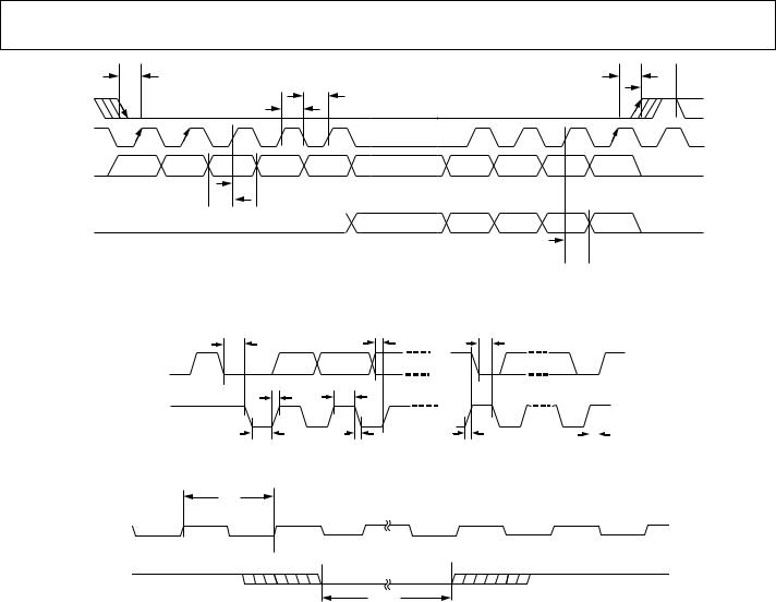
DIGITAL TIMING DIAGRAMS
tBIH
BCLK_IN
tBIL
tLIS
LRCLK_IN
tSIS
SDATA_INX
LEFT-JUSTIFIED MSB MSB-1 MODE
tSIH
tSIS
SDATA_INX
I2S-JUSTIFIED MSB MODE
tSIH
tSIS
SDATA_INX
RIGHT-JUSTIFIED MSB MODE 
tSIH
8-BIT CLOCKS
(24-BIT DATA)
12-BIT CLOCKS
(20-BIT DATA)
14-BIT CLOCKS
(18-BIT DATA)
16-BIT CLOCKS
(16-BIT DATA)
Figure 7. Serial Input Port Timing
tBIH
BCLK_OUTX
tBIL tLOS
LRCLK_OUTX
|
|
|
|
ttSDDMSDDS |
|
|
|
|
|
|
|
|
|
|
|
|
|
|
|
|
|
||
SDATA_OUTX |
|
|
|
|
|
|
|
|
|
|
|
|
|
|
|
|
|
|
|||||
|
|
|
|
|
|
|
|
|
|
|
|
|
|
|
|
|
|||||||
|
|
|
|
|
|
|
|
|
|
|
|
|
|
|
|
|
|
|
|
|
|||
LEFT-JUSTIFIED |
|
|
MSB |
|
|
|
|
|
MSB-1 |
|
|
|
|
|
|
|
|||||||
MODE |
|
|
|
|
|
|
|
|
ttSDDMSDDS |
|
|
|
|
|
|
|
|
|
|
||||
SDATA_OUTX |
|
|
|
|
|
|
|
|
|
|
|
|
|
|
|||||||||
|
|
|
|
|
|
|
|
|
|
|
|
|
|
||||||||||
|
|
|
|
|
|
|
|
|
|||||||||||||||
|
|
|
|
|
|
|
|
|
|
||||||||||||||
|
|
|
|
|
|
|
|
|
|||||||||||||||
I2S-JUSTIFIED |
|
|
|
|
|
|
|
|
|
|
|
|
|
|
|
|
|
|
|
|
|||
|
|
|
|
|
|
|
|
|
|
MSB |
|
||||||||||||
MODE |
|
|
|
|
|
|
|
|
|
|
|
|
|
|
|
|
|
ttSDDMSDDS |
|
|
|||
SDATA_OUTX |
|
|
|
|
|
|
|
|
|
|
|
|
|
|
|
|
|
|
|
||||
|
|
|
|
|
|
|
|
|
|
|
|
|
|
|
|
|
|
||||||
|
|
|
|
|
|
|
|
|
|
|
|
|
|
|
|
|
|
|
|||||
RIGHT-JUSTIFIED |
|
|
|
|
|
|
|
|
|
|
|
|
|
|
|
|
|
|
|
|
|
||
|
|
|
|
|
|
|
|
|
|
|
|
|
|
|
|
|
|
MSB |
|
||||
MODE |
|
|
|
|
|
|
|
|
|
|
|
|
|
|
|
|
|
|
|
|
|
||
8-BIT CLOCKS
(24-BIT DATA)
12-BIT CLOCKS
(20-BIT DATA)
14-BIT CLOCKS
(18-BIT DATA)
16-BIT CLOCKS
(16-BIT DATA)
Figure 8. Serial Output Port Timing
ADAU1701
tLIH
tSIS
LSB
tSIH
04607-0-013
tLCH
tTS
LSB
04607-0-014
Rev. PrC | Page 9 of 39
ADAU1701
|
tCLS |
|
tCCPL |
CLATCH |
tCCPH |
CCLK |
|
CDATA |
|
 tCDH
tCDH
tCDS 
COUT
Figure 9. SPI Port Timing
tTSCH |
tDS |
tTSCH |
SDA |
|
|
tSR |
tSCLH |
|
SCLK |
|
|
tSCLL |
tST |
tSCS |
Figure 10. I2C Port Timing
tMP
MCLK
RESETB
tRLPW
Figure 11. Master Clock and Reset Timing
tCLH
 tCOD
tCOD
tSSH |
|
04607-026 |
|
||
|
|
 tCLPH
tCLPH
04607-0-015
04607-0-016
Rev. PrC | Page 10 of 39
ADAU1701
PIN CONFIGURATION AND FUNCTION DESCRIPTIONS
|
AVDD |
FILTA |
VOUT0 |
VOUT1 |
VOUT2 |
VOUT3 |
AGND |
FILTD |
CM |
PLL_MODE1 |
PLL_MODE0 |
AGND |
|
|
48 |
47 |
46 |
45 |
44 |
43 |
42 |
41 |
40 |
39 |
38 |
37 |
|
AGND |
1 |
|
|
|
|
|
|
|
|
|
|
36 |
AVDD |
ADC1 |
2 |
|
|
|
|
|
|
|
|
|
|
35 |
PLL_LF |
ADC_RES |
3 |
|
|
|
|
|
|
|
|
|
|
34 |
PVDD |
ADC0 |
4 |
|
|
|
|
|
|
|
|
|
|
33 |
PGND |
RESETB |
5 |
|
|
|
ADAU1701 |
|
|
|
32 |
MCLKI |
|||
SELFBOOT |
6 |
|
|
|
|
|
|
31 |
OSCO |
||||
ADDR0 |
7 |
|
|
|
TOP VIEW |
|
|
|
30 |
RSVD |
|||
|
|
|
(Not to Scale) |
|
|
|
|||||||
MP4 |
8 |
|
|
|
|
|
|
29 |
MP2 |
||||
|
|
|
|
|
|
|
|
|
|
||||
MP5 |
9 |
|
|
|
|
|
|
|
|
|
|
28 |
MP3 |
MP1 10 |
|
|
|
|
|
|
|
|
|
|
27 |
MP8 |
|
MP0 11 |
|
|
|
|
|
|
|
|
|
|
26 |
MP9 |
|
DGND 12 |
|
|
|
|
|
|
|
|
|
|
25 |
DGND |
|
|
13 |
14 |
15 |
16 |
17 |
18 |
19 |
20 |
21 |
22 |
23 |
24 |
|
|
DVDD |
MP7 |
MP6 |
MP10 |
VDRIVE |
IOVDD |
MP11 |
ADDR1/CDATA/WB_TRIG |
CLATCH/WP |
SDA/COUT |
SCL/CCLK |
DVDD |
|
Figure 12. 48-Lead LQFP Pin Configuration
Table 11. Pin Function Descriptions
Pin No. |
I/O |
Mnemonic |
Description |
|
|
|
|
1 |
|
AGND |
Analog Ground |
2 |
IN |
ADC1 |
Analog input 1 |
3 |
|
ADC_RES |
Reference current – connect resistor |
4 |
IN |
ADC0 |
Analog Input 0 |
5 |
IN |
RESETB |
Reset, Active Low |
6 |
IN |
SELFBOOT |
Select Host or Self-boot mode |
7 |
IN |
ADDR0 |
I2C and SPI Address 0 |
8 |
IN/OUT |
MP4 |
Multi-Purpose – GPIO or Serial input port LRCLK |
9 |
IN/OUT |
MP5 |
Multi-Purpose – GPIO or Serial input port BCLK |
10 |
IN/OUT |
MP1 |
Multi-Purpose – GPIO or Serial Input port data 1 |
11 |
IN/OUT |
MP0 |
Multi-Purpose – GPIO or Serial Input port data 0 |
12 |
|
DGND |
Digital Ground |
13 |
|
DVDD |
1.8 V Digital Supply |
14 |
IN/OUT |
MP7 |
Multi-Purpose – GPIO or Serial output port data 1 |
15 |
IN/OUT |
MP6 |
Multi-Purpose – GPIO, Serial output port data 0, or TDM data output |
16 |
IN/OUT |
MP10 |
Multi-Purpose – GPIO or Serial output port LRCLK |
17 |
OUT |
VDRIVE |
Drive for external PNP Transistor for 1.8 V regulator |
18 |
|
IOVDD |
Input and Output Pin Supply |
19 |
IN/OUT |
MP11 |
Multi-Purpose – GPIO or Serial output port BCLK |
20 |
IN |
ADDR1/CDATA/WB_TRIG |
I2C Address 1 / SPI Data Input / Self-boot Write-back trigger |
21 |
IN/OUT |
CLATCH / WP |
SPI Latch / Self-boot EEPROM write protect |
22 |
IN/OUT |
SDA/COUT |
I2C Data / SPI Data Out |
23 |
IN/OUT |
SCL/CCLK |
I2C Clock / SPI Clock |
24 |
|
DVDD |
1.8 V Digital Supply |
25 |
|
DGND |
Digital Ground |
Rev. PrC | Page 11 of 39

ADAU1701
26 |
IN/OUT |
MP9 |
Multi-Purpose – GPIO or Aux ADC input 0 |
27 |
IN/OUT |
MP8 |
Multi-Purpose – GPIO or Aux ADC input 3 |
28 |
IN/OUT |
MP3 |
Multi-Purpose – GPIO or Aux ADC input 2 |
29 |
IN/OUT |
MP2 |
Multi-Purpose – GPIO or Aux ADC input 1 |
30 |
|
RSVD |
Reserved, tie to ground |
31 |
OUT |
OSCO |
Oscillator Output |
32 |
IN |
MCLKI |
Master Clock or Crystal Input |
33 |
|
PGND |
PLL Ground |
34 |
|
PVDD |
3.3 V PLL Power |
35 |
|
PLL_LF |
PLL Loop Filter connection |
36 |
|
AVDD |
3.3 V Analog Supply |
37 |
|
AGND |
Analog Ground |
38 |
IN |
PLL_MODE0 |
PLL Mode select 0 |
39 |
IN |
PLL_MODE1 |
PLL Mode select 1 |
40 |
|
CM |
Common Mode Decoupling Capacitor |
41 |
|
FILTD |
Decoupling Capacitor |
42 |
|
AGND |
Analog Ground |
43 |
OUT |
VOUT3 |
Channel 3 DAC output |
44 |
OUT |
VOUT2 |
Channel 2 DAC output |
45 |
OUT |
VOUT1 |
Channel 1 DAC output |
46 |
OUT |
VOUT0 |
Channel 0 DAC output |
47 |
|
FILTA |
Decoupling capacitor |
48 |
|
AVDD |
3.3 V Analog Supply |
Rev. PrC | Page 12 of 39
 Loading...