


 Loading...
Analog Devices AD7730LEB, AD7730EB, AD7730LBRU, AD7730LBR, AD7730BRU Datasheet
...a
Bridge Transducer ADC
AD7730/AD7730L
KEY FEATURES
Resolution of 230,000 Counts (Peak-to-Peak) Offset Drift: 5 nV/8C
Gain Drift: 2 ppm/8C
Line Frequency Rejection: >150 dB Buffered Differential Inputs Programmable Filter Cutoffs Specified for Drift Over Time
Operates with Reference Voltages of 1 V to 5 V
ADDITIONAL FEATURES
Two-Channel Programmable Gain Front End On-Chip DAC for Offset/TARE Removal FASTStep™ Mode
AC or DC Excitation Single Supply Operation
APPLICATIONS
Weigh Scales
Pressure Measurement
GENERAL DESCRIPTION
The modulator output is processed by a low pass programmable digital filter, allowing adjustment of filter cutoff, output rate and settling time.
The part features two buffered differential programmable gain analog inputs as well as a differential reference input. The part operates from a single +5 V supply. It accepts four unipolar analog input ranges: 0 mV to +10 mV, +20 mV, +40 mV and +80 mV and four bipolar ranges: ±10 mV, ±20 mV, ±40 mV and ±80 mV. The peak-to-peak resolution achievable directly from the part is 1 in 230,000 counts. An on-chip 6-bit DAC allows the removal of TARE voltages. Clock signals for synchronizing ac excitation of the bridge are also provided.
The serial interface on the part can be configured for three-wire operation and is compatible with microcontrollers and digital signal processors. The AD7730 contains self-calibration and system calibration options, and features an offset drift of less than 5 nV/°C and a gain drift of less than 2 ppm/°C.
The AD7730 is available in a 24-pin plastic DIP, a 24-lead SOIC and 24-lead TSSOP package. The AD7730L is available in a 24-lead SOIC and 24-lead TSSOP package.
The AD7730 is a complete analog front end for weigh-scale and pressure measurement applications. The device accepts lowlevel signals directly from a transducer and outputs a serial digital word. The input signal is applied to a proprietary programmable gain front end based around an analog modulator.
NOTE
The description of the functions and operation given in this data sheet apply to both the AD7730 and AD7730L. Specifications and performance parameters differ for the parts. Specifications for the AD7730L are outlined in Appendix A.
FUNCTIONAL BLOCK DIAGRAM
|
AVDD |
DVDD |
|
REF IN(–) REF IN(+) |
|
|
|
|
VBIAS |
|
|
|
REFERENCE DETECT |
AD7730 |
|
||
AIN1(+) |
|
AVDD |
|
|
|
SIGMA-DELTA A/D CONVERTER |
STANDBY |
|
|
|
|
|
|
|
|||
AIN1(–) |
100nA |
BUFFER |
|
SIGMA- |
PROGRAMMABLE |
SYNC |
||
|
|
|
|
+ |
|
DELTA |
DIGITAL |
|
|
|
|
|
|
|
|||
|
MUX |
|
|
PGA |
MODULATOR |
FILTER |
|
|
|
|
|
+/– |
|
||||
|
|
|
|
|
|
|
|
|
AIN2(+)/D1 |
100nA |
|
|
|
|
CLOCK |
MCLK IN |
|
|
|
|
6-BIT |
|
|
|||
AIN2(–)/D0 |
|
|
|
|
|
|||
|
AGND |
DAC |
SERIAL INTERFACE |
GENERATION |
MCLK OUT |
|||
|
|
|
|
|
AND CONTROL LOGIC |
|
|
|
|
|
|
|
|
|
|
REGISTER BANK |
SCLK |
|
|
|
|
|
|
|
|
|
|
|
|
|
|
CALIBRATION |
|
CS |
|
|
|
|
|
|
|
DIN |
||
ACX |
AC |
|
|
|
MICROCONTROLLER |
|
||
|
|
|
|
|
|
DOUT |
||
|
EXCITATION |
|
|
|
|
|
||
ACX |
|
|
|
|
|
|
||
CLOCK |
|
|
|
|
|
|
|
|
|
|
AGND |
DGND |
POL |
RDY |
RESET |
|
|
FASTStep is a trademark of Analog Devices, Inc.
REV. A
Information furnished by Analog Devices is believed to be accurate and reliable. However, no responsibility is assumed by Analog Devices for its use, nor for any infringements of patents or other rights of third parties which may result from its use. No license is granted by implication or otherwise under any patent or patent rights of Analog Devices.
One Technology Way, P.O. Box 9106, Norwood, MA 02062-9106, U.S.A.
Tel: 781/329-4700 |
World Wide Web Site: http://www.analog.com |
Fax: 781/326-8703 |
© Analog Devices, Inc., 1998 |
|
(AVDD = +5 V, DVDD = +3 V or +5 V; REF IN(+) = AVDD; REF IN(–) = AGND = DGND = |
||
AD7730–SPECIFICATIONS 0 V; fCLK IN = 4.9152 MHz. All specifications TMIN to TMAX unless otherwise noted.) |
|||
Parameter |
B Version1 |
Units |
Conditions/Comments |
STATIC PERFORMANCE (CHP = 1) |
|
|
|
No Missing Codes2 |
24 |
Bits min |
|
Output Noise and Update Rates2 |
See Tables I & II |
|
|
Integral Nonlinearity |
18 |
ppm of FSR max |
|
Offset Error2 |
See Note 3 |
nV/°C typ |
Offset Error and Offset Drift Refer to Both |
Offset Drift vs. Temperature2 |
5 |
Unipolar Offset and Bipolar Zero Errors |
|
Offset Drift vs. Time4 |
25 |
nV/1000 Hours typ |
|
Positive Full-Scale Error2, 5 |
See Note 3 |
ppm of FS/°C max |
|
Positive Full-Scale Drift vs Temp2, 6, 7 |
2 |
|
|
Positive Full-Scale Drift vs Time4 |
10 |
ppm of FS/1000 Hours typ |
|
Gain Error2, 8 |
See Note 3 |
ppm/°C max |
|
Gain Drift vs. Temperature2, 6, 9 |
2 |
|
|
Gain Drift vs. Time4 |
10 |
ppm/1000 Hours typ |
|
Bipolar Negative Full-Scale Error2 |
See Note 3 |
ppm of FS/°C max |
|
Negative Full-Scale Drift vs. Temp2, 6 |
2 |
|
|
Power Supply Rejection |
120 |
dB typ |
Measured with Zero Differential Voltage |
Common-Mode Rejection (CMR) |
120 |
dB min |
At DC. Measured with Zero Differential Voltage |
Analog Input DC Bias Current2 |
50 |
nA max |
|
Analog Input DC Bias Current Drift2 |
100 |
pA/°C typ |
|
Analog Input DC Offset Current2 |
10 |
nA max |
|
Analog Input DC Offset Current Drift2 |
50 |
pA/°C typ |
|
STATIC PERFORMANCE (CHP = 0)2 |
|
|
SKIP = 010 |
No Missing Codes |
24 |
Bits min |
|
Output Noise and Update Rates |
See Tables III & IV |
|
|
Integral Nonlinearity |
18 |
ppm of FSR max |
|
Offset Error |
See Note 3 |
μV/°C typ |
Offset Error and Offset Drift Refer to Both |
Offset Drift vs. Temperature6 |
0.5 |
Unipolar Offset and Bipolar Zero Errors |
|
Offset Drift vs. Time4 |
2.5 |
μV/1000 Hours typ |
|
Positive Full-Scale Error5 |
See Note 3 |
μV/°C typ |
|
Positive Full-Scale Drift vs. Temp6, 7 |
0.6 |
|
|
Positive Full-Scale Drift vs. Time4 |
3 |
μV/1000 Hours typ |
|
Gain Error8 |
See Note 3 |
ppm/°C typ |
|
Gain Drift vs. Temperature6, 9 |
2 |
|
|
Gain Drift vs. Time4 |
10 |
ppm/1000 Hours typ |
|
Bipolar Negative Full-Scale Error |
See Note 3 |
μV/°C typ |
|
Negative Full-Scale Drift vs. Temp |
0.6 |
|
|
Power Supply Rejection |
90 |
dB typ |
Measured with Zero Differential Voltage |
Common-Mode Rejection (CMR) on AIN |
100 |
dB typ |
At DC. Measured with Zero Differential Voltage |
CMR on REF IN |
120 |
dB typ |
At DC. Measured with Zero Differential Voltage |
Analog Input DC Bias Current |
60 |
nA max |
|
Analog Input DC Bias Current Drift |
150 |
pA/°C typ |
|
Analog Input DC Offset Current |
30 |
nA max |
|
Analog Input DC Offset Current Drift |
100 |
pA/°C typ |
|
ANALOG INPUTS/REFERENCE INPUTS |
|
|
|
Normal-Mode 50 Hz Rejection2 |
88 |
dB min |
From 49 Hz to 51 Hz |
Normal-Mode 60 Hz Rejection2 |
88 |
dB min |
From 59 Hz to 61 Hz |
Common-Mode 50 Hz Rejection2 |
120 |
dB min |
From 49 Hz to 51 Hz |
Common-Mode 60 Hz Rejection2 |
120 |
dB min |
From 59 Hz to 61 Hz |
Analog Inputs |
|
|
|
Differential Input Voltage Ranges11 |
|
|
Assuming 2.5 V or 5 V Reference with |
|
0 to +10 or ±10 |
|
HIREF Bit Set Appropriately |
|
mV nom |
Gain = 250 |
|
|
0 to +20 or ±20 |
mV nom |
Gain = 125 |
|
0 to +40 or ±40 |
mV nom |
Gain = 62.5 |
Absolute/Common-Mode Voltage12 |
0 to +80 or ±80 |
mV nom |
Gain = 31.25 |
AGND + 1.2 V |
V min |
|
|
Reference Input |
AVDD – 0.95 V |
V max |
|
|
|
|
|
REF IN(+) – REF IN(–) Voltage |
+2.5 |
V nom |
HIREF Bit of Mode Register = 0 |
REF IN(+) – REF IN(–) Voltage |
+5 |
V nom |
HIREF Bit of Mode Register = 1 |
Absolute/Common-Mode Voltage13 |
AGND – 30 mV |
V min |
|
|
AVDD + 30 mV |
V max |
NO REF Bit Active If VREF Below This Voltage |
NO REF Trigger Voltage |
0.3 |
V min |
|
|
0.65 |
V max |
NO REF Bit Inactive If VREF Above This Voltage |
–2– |
REV. A |
AD7730/AD7730L
Parameter |
B Version1 |
Units |
Conditions/Comments |
LOGIC INPUTS |
±10 |
μA max |
|
Input Current |
|
||
All Inputs Except SCLK and MCLK IN |
|
|
|
VINL, Input Low Voltage |
0.8 |
V max |
DVDD = +5 V |
VINL, Input Low Voltage |
0.4 |
V max |
DVDD = +3 V |
VINH, Input High Voltage |
2.0 |
V min |
|
SCLK Only (Schmitt Triggered Input) |
|
|
|
VT+ |
1.4/3 |
V min to V max |
DVDD = +5 V |
VT+ |
1/2.5 |
V min to V max |
DVDD = +3 V |
VT– |
0.8/1.4 |
V min to V max |
DVDD = +5 V |
VT– |
0.4/1.1 |
V min to V max |
DVDD = +3 V |
VT+ – VT– |
0.4/0.8 |
V min to V max |
DVDD = +5 V |
VT+ – VT– |
0.4/0.8 |
V min to V max |
DVDD = +3 V |
MCLK IN Only |
|
|
|
VINL, Input Low Voltage |
0.8 |
V max |
DVDD = +5 V |
VINL, Input Low Voltage |
0.4 |
V max |
DVDD = +3 V |
VINH, Input High Voltage |
3.5 |
V min |
DVDD = +5 V |
VINH, Input High Voltage |
2.5 |
V min |
DVDD = +3 V |
LOGIC OUTPUTS (Including MCLK OUT) |
|
|
ISINK = 800 μA Except for MCLK OUT14; |
VOL, Output Low Voltage |
|
|
|
|
0.4 |
V max |
VDD15 = +5 V |
VOL, Output Low Voltage |
|
|
ISINK = 100 μA Except for MCLK OUT14; |
|
0.4 |
V max |
VDD15 = +3 V |
VOH, Output High Voltage |
|
|
ISOURCE = 200 μA Except for MCLK OUT14; |
|
4.0 |
V min |
VDD15 = +5 V |
VOH, Output High Voltage |
|
|
ISOURCE = 100 μA Except for MCLK OUT14; |
|
VDD – 0.6 V |
V min |
VDD15 = +3 V |
Floating State Leakage Current |
±10 |
μA max |
|
Floating State Output Capacitance2 |
6 |
pF typ |
|
TRANSDUCER BURNOUT |
|
|
|
AIN1(+) Current |
–100 |
nA nom |
|
AIN1(–) Current |
100 |
nA nom |
|
Initial Tolerance @ 25°C |
±10 |
% typ |
|
Drift2 |
0.1 |
%/°C typ |
|
OFFSET (TARE) DAC |
|
|
|
Resolution |
6 |
Bit |
|
LSB Size |
2.3/2.6 |
mV min/mV max |
2.5 mV Nominal with 5 V Reference (REF IN/2000) |
DAC Drift16 |
2.5 |
ppm/°C max |
|
DAC Drift vs. Time4, 16 |
25 |
ppm/1000 Hours typ |
|
Differential Linearity |
–0.25/+0.75 |
LSB max |
Guaranteed Monotonic |
|
|
|
|
SYSTEM CALIBRATION |
1.05 × FS |
|
|
Positive Full-Scale Calibration Limit17 |
V max |
FS Is the Nominal Full-Scale Voltage |
|
Negative Full-Scale Calibration Limit17 |
–1.05 × FS |
|
(10 mV, 20 mV, 40 mV or 80 mV) |
V max |
|
||
Offset Calibration Limit18 |
–1.05 × FS |
V max |
|
Input Span17 |
0.8 × FS |
V min |
|
|
2.1 × FS |
V max |
|
POWER REQUIREMENTS |
|
|
|
Power Supply Voltages |
|
|
|
AVDD – AGND Voltage |
+4.75 to +5.25 |
V min to V max |
|
DVDD Voltage |
+2.7 to +5.25 |
V min to V max |
With AGND = 0 V |
Power Supply Currents |
|
|
External MCLK. Digital I/Ps = 0 V or DVDD |
AVDD Current (Normal Mode) |
10.3 |
mA max |
All Input Ranges Except 0 mV to +10 mV and ±10 mV |
AVDD Current (Normal Mode) |
22.3 |
mA max |
Input Ranges of 0 mV to +10 mV and ±10 mV Only |
DVDD Current (Normal Mode) |
1.3 |
mA max |
DVDD of 2.7 V to 3.3 V |
DVDD Current (Normal Mode) |
2.7 |
mA max |
DVDD of 4.75 V to 5.25 V |
AVDD + DVDD Current (Standby Mode) |
25 |
μA max |
Typically 10 μA. External MCLK IN = 0 V or DVDD |
Power Dissipation |
|
|
AVDD = DVDD = +5 V. Digital I/Ps = 0 V or DVDD |
Normal Mode |
65 |
mW max |
All Input Ranges Except 0 mV to +10 mV and ±10 mV |
|
125 |
mW max |
Input Ranges of 0 mV to +10 mV and ±10 mV Only |
Standby Mode |
125 |
μW max |
Typically 50 μW. External MCLK IN = 0 V or DVDD |
REV. A |
–3– |
AD7730/AD7730L
NOTES
1Temperature range: –40°C to +85°C.
2Sample tested during initial release.
3The offset (or zero) numbers with CHP = 1 are typically 3 μV precalibration. Internal zero-scale calibration reduces this by about 1 μV. Offset numbers with CHP = 0 can be up to 1 mV precalibration. Internal zero-scale calibration reduces this to 2 μV typical. System zero-scale calibration reduces offset numbers with CHP = 1 and CHP = 0 to the order of the
noise. Gain errors can be up to 3000 ppm precalibration with CHP = 0 and CHP = 1. Performing internal full-scale calibrations on the 80 mV range reduces the gain error to less than 100 ppm for the 80 mV and 40 mV ranges, to about 250 ppm for the 20 mV range and to about 500 ppm on the 10 mV range. System full-scale calibration reduces this to the order of the noise. Positive and negative full-scale errors can be calculated from the offset and gain errors.
4These numbers are generated during life testing of the part.
5Positive Full-Scale Error includes Offset Errors (Unipolar Offset Error or Bipolar Zero Error) and applies to both unipolar and bipolar input ranges. See Terminology. 6Recalibration at any temperature will remove these errors.
7Full-Scale Drift includes Offset Drift (Unipolar Offset Drift or Bipolar Zero Drift) and applies to both unipolar and bipolar input ranges.
8Gain Error is a measure of the difference between the measured and the ideal span between any two points in the transfer function. The two points used to calculate the gain error are positive full scale and negative full scale. See Terminology.
9Gain Error Drift is a span drift and is effectively the drift of the part if zero-scale calibrations only were performed.
10No Missing Codes performance with CHP = 0 and SKIP = 1 is reduced below 24 bits for SF words lower than 180 decimal.
11The analog input voltage range on the AIN1(+) and AIN2(+) inputs is given here with respect to the voltage on the AIN1(–) and AIN2(–) inputs respectively. 12The common-mode voltage range on the input pairs applies provided the absolute input voltage specification is obeyed.
13The common-mode voltage range on the reference input pair (REF IN(+) and REF IN(–)) applies provided the absolute input voltage specification is obeyed. 14These logic output levels apply to the MCLK OUT output only when it is loaded with a single CMOS load.
15VDD refers to DVDD for all logic outputs expect D0, D1, ACX and ACX where it refers to AVDD. In other words, the output logic high for these four outputs is determined by AVDD. 16This number represents the total drift of the channel with a zero input and the DAC output near full scale.
17After calibration, if the input voltage exceeds positive full scale, the converter will output all 1s. If the input is less than negative full scale, the device outputs all 0s.
18These calibration and span limits apply provided the absolute input voltage specification is obeyed. The offset calibration limit applies to both the unipolar zero point and the bipolar zero point.
Specifications subject to change without notice.
|
1, 2 |
(AVDD = +4.75 V to +5.25 V; DVDD = +2.7 V to +5.25 V; AGND = DGND = 0 V; fCLK IN = 4.9152 MHz; |
||
TIMING CHARACTERISTICS |
Input Logic 0 = 0 V, Logic 1 = DVDD unless otherwise noted). |
|||
|
Limit at TMIN to TMAX |
|
|
|
Parameter |
(B Version) |
|
Units |
Conditions/Comments |
|
|
|
|
|
Master Clock Range |
1 |
|
MHz min |
For Specified Performance |
|
5 |
|
MHz max |
|
t1 |
50 |
|
ns min |
SYNC Pulsewidth |
t2 |
50 |
|
ns min |
RESET Pulsewidth |
Read Operation |
|
|
|
|
t3 |
0 |
|
ns min |
RDY to CS Setup Time |
t4 |
0 |
|
ns min |
CS Falling Edge to SCLK Active Edge Setup Time3 |
t54 |
0 |
|
ns min |
SCLK Active Edge to Data Valid Delay3 |
|
60 |
|
ns max |
DVDD = +4.75 V to +5.25 V |
t5A4, 5 |
80 |
|
ns max |
DVDD = +2.75 V to +3.3 V |
0 |
|
ns min |
CS Falling Edge to Data Valid Delay |
|
|
60 |
|
ns max |
DVDD = +4.75 V to +5.25 V |
t6 |
80 |
|
ns max |
DVDD = +2.7 V to +3.3 V |
100 |
|
ns min |
SCLK High Pulsewidth |
|
t7 |
100 |
|
ns min |
SCLK Low Pulsewidth |
t8 |
0 |
|
ns min |
CS Rising Edge to SCLK Inactive Edge Hold Time3 |
t96 |
10 |
|
ns min |
Bus Relinquish Time after SCLK Inactive Edge3 |
|
80 |
|
ns max |
SCLK Active Edge to RDY High3, 7 |
t10 |
100 |
|
ns max |
|
Write Operation |
|
|
|
CS Falling Edge to SCLK Active Edge Setup Time3 |
t11 |
0 |
|
ns min |
|
t12 |
30 |
|
ns min |
Data Valid to SCLK Edge Setup Time |
t13 |
25 |
|
ns min |
Data Valid to SCLK Edge Hold Time |
t14 |
100 |
|
ns min |
SCLK High Pulsewidth |
t15 |
100 |
|
ns min |
SCLK Low Pulsewidth |
t16 |
0 |
|
ns min |
CS Rising Edge to SCLK Edge Hold Time |
NOTES
1Sample tested during initial release to ensure compliance. All input signals are specified with tr = tf = 5 ns (10% to 90% of DV DD) and timed from a voltage level of 1.6 V. 2See Figures 18 and 19.
3SCLK active edge is falling edge of SCLK with POL = 1; SCLK active edge is rising edge of SCLK with POL = 0.
4These numbers are measured with the load circuit of Figure 1 and defined as the time required for the output to cross the VOL or VOH limits.
5This specification only comes into play if CS goes low while SCLK is low (POL = 1) or if CS goes low while SCLK is high (POL = 0). It is primarily required for interfacing to DSP machines.
6These numbers are derived from the measured time taken by the data output to change 0.5 V when loaded with the circuit of Figure 1. The measured number is then extrapolated back to remove effects of charging or discharging the 50 pF capacitor. This means that the times quoted in the timing characteristics are the true bus relinquish times of the part and as such are independent of external bus loading capacitances.
7RDY returns high after the first read from the device after an output update. The same data can be read again, if required, while RDY is high, although care should be taken that subsequent reads do not occur close to the next output update.
–4– |
REV. A |
AD7730/AD7730L
ABSOLUTE MAXIMUM RATINGS*
(TA = +25°C unless otherwise noted)
AVDD to AGND . . . . . . . . . . . . |
. . . . . . . . . . . –0.3 V to +7 V |
AVDD to DGND . . . . . . . . . . . . |
. . . . . . . . . . . –0.3 V to +7 V |
DVDD to AGND . . . . . . . . . . . . |
. . . . . . . . . . . –0.3 V to +7 V |
DVDD to DGND . . . . . . . . . . . . |
. . . . . . . . . . . –0.3 V to +7 V |
AGND to DGND . . . . . . . . . . . |
. . . . . . . . . . . –5 V to +0.3 V |
AVDD to DVDD . . . . . . . . . . . . . |
. . . . . . . . . . . . –2 V to +5 V |
Analog Input Voltage to AGND |
. . . . –0.3 V to AVDD + 0.3 V |
Reference Input Voltage to AGND . . –0.3 V to AVDD + 0.3 V
AIN/REF IN Current (Indefinite) |
. . . . . . . . . . . . . . . . 30 mA |
||
Digital Input Voltage to DGND |
. . . . –0.3 V to DVDD + 0.3 |
V |
|
Digital Output Voltage to DGND |
. . . –0.3 V to DVDD + 0.3 |
V |
|
Output Voltage (ACX, ACX, D0, D1) to DGND |
|
||
Operating. . . . . . Temperature. . . . . . . . . . .Range. . . . . . . |
. . . . –0.3 V to AVDD + 0.3 |
V |
|
–40°C to +85°C |
|||
Industrial (B Version) . . . . . . |
|||
Storage Temperature Range . . |
. . . . . . . . . –65°C to +150°C |
||
Junction Temperature . . . . . . . . |
. . . . . . . . . . . . . . . . +150°C |
||
Plastic DIP Package, Power Dissipation . . . . . . . 450 mW
θJA Thermal Impedance . . . . . . . . . . . . . . . . . 105°C/W Lead Temperature (Soldering, 10 sec) . . . . . . . +260°C
TSSOP Package, Power Dissipation . . . . . . . . . . 450 mW
θJA Thermal Impedance . . . . . . . . . . . . . . . . . 128°C/W Lead Temperature, Soldering
Vapor Phase (60 sec) . . . . . . . . . . . . . . . . . . +215°C Infrared (15 sec) . . . . . . . . . . . . . . . . . . . . . . +220°C SOIC Package, Power Dissipation . . . . . . . . . . . . 450 mW
θJA Thermal Impedance . . . . . . . . . . . . . . . . . . 75°C/W Lead Temperature, Soldering
Vapor Phase (60 sec) . . . . . . . . . . . . . . . . . . +215°C Infrared (15 sec) . . . . . . . . . . . . . . . . . . . . . . +220°C
*Stresses above those listed under Absolute Maximum Ratings may cause permanent damage to the device. This is a stress rating only; functional operation of the device at these or any other conditions above those listed in the operational sections of this specification is not implied. Exposure to absolute maximum rating conditions for extended periods may affect device reliability.
ORDERING GUIDE
|
Temperature |
Package |
Package |
Model |
Range |
Description |
Options |
|
|
|
|
AD7730BN |
–40°C to +85°C |
Plastic DIP |
N-24 |
AD7730BR |
–40°C to +85°C |
Small Outline |
R-24 |
AD7730BRU |
–40°C to +85°C |
Thin Shrink Small Outline |
RU-24 |
EVAL-AD7730EB |
Evaluation Board |
|
|
AD7730LBR |
–40°C to +85°C |
Small Outline |
R-24 |
AD7730LBRU |
–40°C to +85°C |
Thin Shrink Small Outline |
RU-24 |
EVAL-AD7730LEB |
Evaluation Board |
|
|
|
|
|
|
ISINK (800mA AT DVDD = +5V |
100mA AT DVDD = +3V) |
TO OUTPUT |
+1.6V |
|
PIN |
||
|
||
|
50pF |
 ISOURCE (200mA AT DVDD = +5V
100mA AT DVDD = +3V)
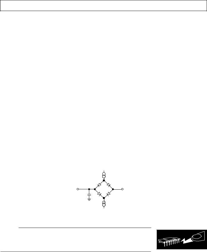
Figure 1. Load Circuit for Access Time and Bus Relinquish Time
CAUTION
ESD (electrostatic discharge) sensitive device. Electrostatic charges as high as 4000 V readily accumulate on the human body and test equipment and can discharge without detection. Although the AD7730 features proprietary ESD protection circuitry, permanent damage may occur on devices subjected to high energy electrostatic discharges. Therefore, proper ESD precautions are recommended to avoid performance degradation or loss of functionality.
WARNING! |
ESD SENSITIVE DEVICE |
REV. A |
–5– |

AD7730/AD7730L
|
|
|
|
|
|
|
DIFFERENTIAL |
|
|
|
|
|
PROGRAMMABLE |
|
BUFFER AMPLIFIER |
|
|
PROGRAMMABLE GAIN |
|
|
|
REFERENCE |
|
|
SIGMA-DELTA ADC |
|
|
DIGITAL FILTER |
|
|
|
|
AMPLIFIER |
|
|
|
|
|
|
SIGMA DELTA ADC |
|
|
|
|
THE BUFFER AMPLIFIER |
|
|
|
|
|
|
THE REFERENCE INPUT TO THE |
|
|
THE SIGMA-DELTA |
|
|
TWO STAGE FILTER THAT |
|
PRESENTS A HIGH IMPEDANCE |
|
|
THE PROGRAMMABLE GAIN |
|
|
|
PART IS DIFFERENTIAL AND |
|
|
THE SIGMA DELTA |
|
|
ALLOWS PROGRAMMING OF |
|
|
|
|
|
|
|
|
ARCHITECTURE ENSURES 24 BITS |
|
|
|
||||
INPUT STAGE FOR THE ANALOG |
|
|
AMPLIFIER ALLOWS FOUR |
|
|
|
FACILITATES RATIOMETRIC |
|
|
ARCHITECTURE ENSURES 24 BITS |
|
|
OUTPUT UPDATE RATE AND |
|
|
|
|
|
|
|
|
NO MISSING CODES. THE |
|
|
|
||||
INPUTS ALLOWING SIGNIFICANT |
|
|
UNIPOLAR AND FOUR BIPOLAR |
|
|
|
OPERATION. THE REFERENCE |
|
|
NO MISSING CODES. THE |
|
|
SETTLING TIME AND WHICH HAS |
|
|
|
|
|
|
|
|
ENTIRE SIGMA-DELTA ADC CAN |
|
|
|
||||
EXTERNAL SOURCE |
|
|
INPUT RANGES FROM |
|
|
|
VOLTAGE CAN BE SELECTED TO |
|
|
ENTIRE SIGMA DELTA. ADC CAN |
|
|
A FAST STEP MODE |
|
|
|
|
|
|
|
|
BE CHOPPED TO REMOVE DRIFT |
|
|
|
||||
IMPEDANCES |
|
|
+10mV TO +80mV |
|
|
|
BE NOMINALLY +2.5V OR +5V |
|
|
BE CHOPPED TO REMOVE DRIFT |
|
|
(SEE FIGURE 3) |
|
|
|
|
|
|
|
|
ERRORS |
|
|
|
||||
|
|
|
|
|
|
|
|
|
|
ERRORS |
|
|
|
|
SEE PAGE 24 |
|
|
SEE PAGE 24 |
|
|
|
SEE PAGE 25 |
|
|
SEE PAGE 26 |
|
|
SEE PAGE 26 |
|
|
|
|
|
|
|
|
|
|
|
SEE PAGE |
|
|
|
|
BURNOUT CURRENTS
TWO 100nA BURNOUT |
|
|
|
|
|
|
|
|
|
|
|
CURRENTS ALLOW THE USER |
|
|
|
|
|
|
|
|
|
|
|
TO EASILY DETECT IF A |
|
AVDD |
DVDD |
|
REF IN(–) REF IN(+) |
|
|
|
STANDBY MODE |
||
TRANSDUCER HAS BURNT |
|
|
|
|
|
||||||
OUT OR GONE OPEN-CIRCUIT |
|
|
|
|
|
|
|
|
|
|
THE STANDBY MODE REDUCES |
SEE PAGE 25 |
VBIAS |
|
|
|
REFERENCE DETECT |
AD7730 |
|
||||
|
|
|
|
POWER CONSUMPTION TO 5mA |
|||||||
|
|
|
|
|
|
|
|
|
|
|
|
|
|
|
AVDD |
|
|
|
|
|
|
STANDBY |
SEE PAGE 33 |
AIN1(+) |
|
|
|
|
|
SIGMA-DELTA A/D CONVERTER |
|
||||
|
|
|
|
|
|
|
|||||
AIN1(–) |
|
|
|
|
|
|
SIGMA- |
PROGRAMMABLE |
SYNC |
CLOCK OSCILLATOR |
|
|
|
|
|
|
+ |
|
|
DELTA |
DIGITAL |
||
|
|
|
|
|
|
|
|
CIRCUIT |
|||
|
|
MUX |
|
|
PGA |
MODULATOR |
FILTER |
|
|||
|
|
|
|
+/– |
|
|
|||||
|
|
|
|
|
|
|
|
|
|
THE CLOCK SOURCE FOR THE |
|
|
|
|
|
BUFFER |
|
|
|
|
|
||
AIN2(+)/D1 |
|
|
|
|
|
|
|
PART CAN BE PROVIDED BY AN |
|||
|
|
|
|
|
|
|
CLOCK |
MCLK IN |
EXTERNALLY-APPLIED CLOCK OR |
||
|
|
|
|
6-BIT |
|
|
|
||||
AIN2(–)/D0 |
|
|
|
|
|
BY CONNECTING A CRYSTAL OR |
|||||
|
AGND |
SERIAL INTERFACE |
GENERATION |
MCLK OUT |
|||||||
|
DAC |
CERAMIC RESONATOR ACROSS |
|||||||||
|
|
|
|
|
|
AND CONTROL LOGIC |
|
|
THE CLOCK PINS |
||
|
|
|
|
|
|
|
|
|
REGISTER BANK |
SCLK |
SEE PAGE 32 |
|
|
|
|
|
|
|
|
|
|
|
|
ANALOG MULTIPLEXER |
|
|
|
|
|
|
CALIBRATION |
|
CS |
|
|
|
|
|
|
|
|
|
|
|
|||
|
|
|
|
|
|
MICROCONTROLLER |
|
DIN |
|
||
|
ACX |
AC |
|
|
|
|
|
|
|||
A TWO-CHANNEL DIFFERENTIAL |
|
|
|
|
|
|
|
DOUT |
|
||
|
EXCITATION |
|
|
|
|
|
|
|
|||
MULTIPLEXER SWITCHES ONE OF |
ACX |
|
|
|
|
|
|
|
|
||
CLOCK |
|
|
|
|
|
|
|
|
|
||
THE TWO DIFFERENTIAL INPUT |
|
|
|
|
|
|
|
|
|
||
CHANNELS TO THE BUFFER |
|
|
|
|
|
|
|
|
|
|
SERIAL INTERFACE |
AMPLIFIER. THE MULTIPLEXER IS |
|
|
|
|
|
|
|
|
|
|
|
CONTROLLED VIA THE SERIAL |
|
|
AGND |
DGND |
|
POL |
RDY |
RESET |
|
SPI*-COMPATIBLE OR DSP- |
|
INTERFACE |
|
|
|
|
|||||||
|
|
|
|
|
|
|
|
|
|
COMPATIBLE SERIAL INTERFACE |
|
|
|
|
|
|
|
|
|
|
|
|
|
SEE PAGE 24 |
|
|
|
|
|
|
|
|
|
|
WHICH CAN BE OPERATED FROM |
|
|
|
|
|
|
|
|
|
|
JUST THREE WIRES. ALL |
|
|
|
|
|
|
|
|
|
|
|
|
FUNCTIONS ON THE PART |
|
|
|
|
|
|
|
|
|
|
|
CAN BE ACCESSED VIA |
|
|
|
|
|
|
|
|
|
|
|
THE SERIAL INTERFACE |
|
|
|
|
|
|
|
|
|
|
|
SEE PAGE 35 |
AC EXCITATION
FOR AC-EXCITED BRIDGE APPLICATIONS, THE ACX OUTPUTS PROVIDE SIGNALS THAT CAN BE USED TO SWITCH THE POLARITY OF THE BRIDGE EXCITATION VOLTAGE
SEE PAGE 41
OUTPUT DRIVERS |
|
OFFSET/TARE DAC |
|
REGISTER BANK |
|
THE SECOND ANALOG INPUT |
|
ALLOWS A PROGRAMMED |
|
THIRTEEN REGISTERS CONTROL |
|
CHANNEL CAN BE |
|
VOLTAGE TO BE EITHER ADDED |
|
ALL FUNCTIONS ON THE PART AND |
|
RECONFIGURED TO BECOME TWO |
|
OR SUBTRACTED FROM THE |
|
PROVIDE STATUS INFORMATION |
|
OUTPUT DIGITAL PORT LINES |
|
ANALOG INPUT SIGNAL BEFORE |
|
AND CONVERSION RESULTS |
|
WHICH CAN BE PROGRAMMED |
|
IT IS APPLIED TO THE PGA |
|
|
|
OVER THE SERIAL INTERFACE |
|
SEE PAGE 24 |
|
SEE PAGE 11 |
|
SEE PAGE 33 |
|
|
*SPI IS A TRADEMARK OF MOTOROLA, INC. |
||
|
|
|
|||
|
|
|
|
||
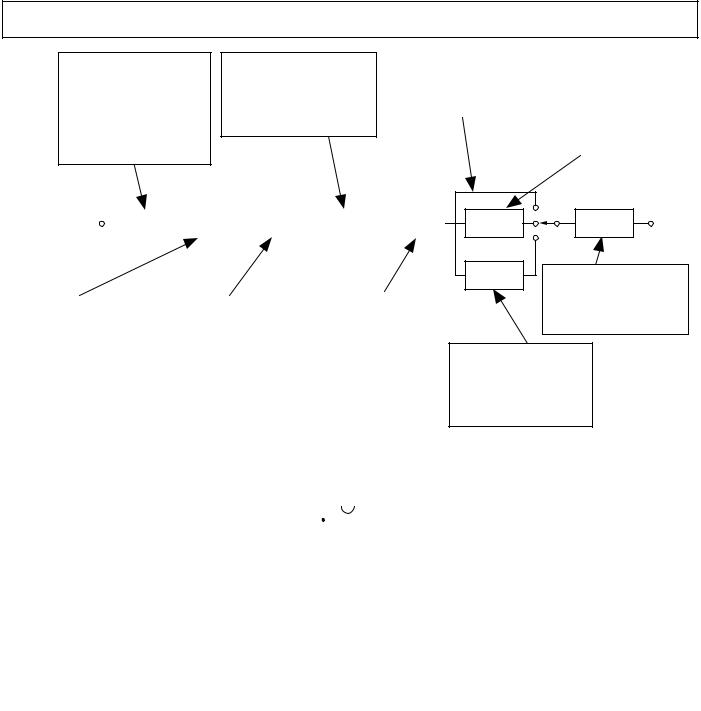
Figure 2. Detailed Functional Block Diagram
–6– |
REV. A |
AD7730/AD7730L
INPUT CHOPPING
THE ANALOG INPUT TO THE PART CAN BE CHOPPED. IN CHOPPING MODE, WITH AC EXCITATION DISABLED, THE INPUT
CHOPPING IS INTERNALTO THE DEVICE. IN CHOPPING MODE, WITH AC EXCITATION ENABLED, THE CHOPPING IS ASSUMED
TO BE PERFORMED EXTERNAL TO THE PART AND NO INTERNAL INPUT CHOPPING IS PERFORMED. THE INPUT CHOPPING CAN BE DISABLED, IF DESIRED.
SEE PAGE 26
SINC3 FILTER
THE FIRST STAGE OF THE DIGITAL FILTERING ON THE PART IS THE SINC3 FILTER. THE OUTPUT UPDATE RATE AND BANDWIDTH OF THIS FILTER CAN BE PROGRAMMED. IN
SKIP MODE, THE SINC3 FILTER IS THE ONLY FILTERING PERFORMED ON THE PART.
SEE PAGE 26
|
SKIP MODE |
|
|
|
22-TAP FIR FILTER |
|
|
IN SKIP MODE, THERE IS NO SECOND |
|
|
|
IN NORMAL OPERATING MODE, THE |
|
|
|
|
|
SECOND STAGE OF THE DIGITAL FILTERING |
|
|
|
STAGE OF FILTERING ON THE PART. THE |
|
|
|
|
|
|
|
|
|
ON THE PART IS A FIXED 22-TAP FIR |
|
|
|
SINC3 FILTER IS THE ONLY FILTERING |
|
|
|
|
|
|
PERFORMED ON THE PART. |
|
|
|
FILTER. IN SKIP MODE, THIS FIR FILTER IS |
|
|
|
|
|
BYPASSED. WHEN FASTSTEP™ MODE IS |
|
|
|
|
|
|
|
|
|
|
SEE PAGE 29 |
|
|
|
ENABLED AND A STEP INPUT IS |
|
|
|
|
|
DETECTED, THE SECOND STAGE FILTERING |
|
|
|
|
|
|
|
|
|
|
|
|
|
|
IS PERFORMED BY THE FILTER |
|
|
|
|
|
|
UNTIL THE OUTPUT OF THIS FILTER |
|
|
|
|
|
|
HAS FULLY SETTLED. |
|
|
|
|
|
|
SEE PAGE 27 |
|
|
|
|
|
|
|
|
ANALOG |
|
|
|
|
|
|
PGA + |
|
|
|
|
|
|
CHOP |
|
BUFFER |
|
SIGMA-DELTA |
|
SINC3 FILTER |
|
CHOP |
|
|
|
|
|
|
|||||||
INPUT |
|
|
|
|
MODULATOR |
|
|
|
|
||
|
BUFFER |
|
|
PGA + SIGMA-DELTA MODULATOR |
|
|
OUTPUT CHOPPING |
|
|
THE INPUT SIGNAL IS BUFFERED |
|
|
THE PROGRAMMABLE GAIN CAPABILITY |
|
|
THE OUTPUT OF THE FIRST STAGE |
|
|
ON-CHIP BEFORE BEING APPLIED TO |
|
|
OF THE PART IS INCORPORATED |
|
|
OF FILTERING ON THE PART CAN |
|
|
THE SAMPLING CAPACITOR OF THE |
|
|
AROUND THE SIGMA-DELTA MODULATOR. |
|
|
BE CHOPPED. IN CHOPPING MODE, |
|
|
SIGMA-DELTA MODULATOR. THIS |
|
|
THE MODULATOR PROVIDES A HIGH- |
|
|
REGARDLESS OF WHETHER AC |
|
|
ISOLATES THE SAMPLING CAPACITOR |
|
|
FREQUENCY 1-BIT DATA STREAM |
|
|
EXCITATION IS ENABLED OR DISABLED, |
|
|
CHARGING CURRENTS FROM THE |
|
|
TO THE DIGITAL FILTER. |
|
|
THE OUTPUT CHOPPING IS |
|
|
ANALOG INPUT PINS. |
|
|
|
|
|
PERFORMED. THE CHOPPING CAN |
|
|
SEE PAGE 24 |
|
|
SEE PAGE 26 |
|
|
BE DISABLED, IF DESIRED. |
|
|
|
|
|
|
|
SEE PAGE 26 |
|
|
|
|
|
|
|||||
|
|
|
|
|
|
|
|
|
|
|
|
|
|
|
|
|
|
|
|
|
|
|
|
|
|
|
SKIP |
|
|
|
22-TAP |
|
OUTPUT |
DIGITAL |
FIR FILTER |
|
SCALING |
OUTPUT |
FASTSTEP |
OUTPUT SCALING |
|
|
FILTER |
|
||
|
|
|
|
THE OUTPUT WORD FROM THE DIGITAL |
|||
FILTER IS SCALED BY THE CALIBRATION |
|||
COEFFICIENTS BEFORE BEING PROVIDED |
|||
AS THE CONVERSION RESULT. |
|||
|
|
SEE PAGE 29 |
|
FASTSTEP FILTER |
|
|
|
WHEN FASTSTEP MODE IS ENABLED |
|
|
|
AND A STEP CHANGE ON THE INPUT |
|
|
|
HAS BEEN DETECTED, THE SECOND |
|
|
|
STAGE FILTERING IS PERFORMED BY THE |
|
||
FASTSTEP FILTER UNTIL THE FIR |
|
|
|
FILTER HAS FULLY SETTLED. |
|
|
|
SEE PAGE 29
Figure 3. Signal Processing Chain
PIN CONFIGURATION
|
|
|
|
|
|
|
|
SCLK |
1 |
|
|
|
24 |
DGND |
|
|
|
|
|
|
|
DVDD |
|
|
|
|
|
|
|
||
MCLK IN |
2 |
|
|
|
23 |
||
|
|
|
|
|
|
|
|
MCLK OUT |
3 |
|
|
|
22 |
DIN |
|
|
|
|
|
|
|
|
|
|
|
|
|
|
|
|
|
POL |
4 |
|
|
|
21 |
DOUT |
|
|
|
|
|
|
|
|
|
|
|
|
|
|
|
|
|
SYNC |
5 |
AD7730 |
20 |
RDY |
|||
|
|
|
|
||||
RESET |
6 |
19 |
CS |
||||
TOP VIEW |
|||||||
VBIAS |
|
|
|
||||
|
|
|
|||||
7 |
(Not to Scale) |
18 |
STANDBY |
||||
|
|
|
|
|
|
|
|
AGND |
8 |
|
|
|
17 |
ACX |
|
|
|
|
|
|
|
|
|
AVDD |
9 |
|
|
|
16 |
ACX |
|
|
|
|
|
|
|
REF IN(–) |
|
AIN1(+) |
10 |
|
|
|
15 |
||
|
|
|
|
|
|
|
|
|
|
|
|
|
|
||
AIN1(–) |
11 |
|
|
|
14 |
REF IN(+) |
|
|
|
|
|
|
|
|
|
|
|
|
|
|
|
|
|
AIN2(+)/D1 |
12 |
|
|
|
13 |
AIN2(–)/D0 |
|
|
|
|
|
|
|
|
|
|
|
PIN FUNCTION DESCRIPTIONS |
|
|
|
Pin |
|
|
No. |
Mnemonic |
Function |
|
|
|
1 |
SCLK |
Serial Clock. Schmitt-Triggered Logic Input. An external serial clock is applied to this input to transfer serial |
|
|
data to or from the AD7730. This serial clock can be a continuous clock with all data transmitted in a con- |
|
|
tinuous train of pulses. Alternatively, it can be a noncontinuous clock with the information being transmitted |
|
|
to or from the AD7730 in smaller batches of data. |
2 |
MCLK IN |
Master Clock signal for the device. This can be provided in the form of a crystal/resonator or external clock. A |
|
|
crystal/resonator can be tied across the MCLK IN and MCLK OUT pins. Alternatively, the MCLK IN pin |
|
|
can be driven with a CMOS-compatible clock and MCLK OUT left unconnected. The AD7730 is specified |
|
|
with a clock input frequency of 4.9152 MHz while the AD7730L is specified with a clock input frequency of |
|
|
2.4576 MHz. |
|
|
|
REV. A |
–7– |
AD7730/AD7730L
Pin |
|
|
|
|
No. |
Mnemonic |
Function |
|
|
|
|
|
|
|
3 |
MCLK OUT |
When the master clock for the device is a crystal/resonator, the crystal/resonator is connected between MCLK IN |
||
|
|
and MCLK OUT. If an external clock is applied to the MCLK IN, MCLK OUT provides an inverted clock sig- |
||
|
|
nal. This clock can be used to provide a clock source for external circuits and MCLK OUT is capable of driving |
||
|
|
one CMOS load. If the user does not require it, MCLK OUT can be turned off with the CLKDIS bit of the Mode |
||
|
|
Register. This ensures that the part is not burning unnecessary power driving capacitance on the MCLK OUT pin. |
||
4 |
POL |
Clock Polarity. Logic Input. This determines the polarity of the serial clock. If the active edge for the proces- |
||
|
|
sor is a high-to-low SCLK transition, this input should be low. In this mode, the AD7730 puts out data on the |
||
|
|
DATA OUT line in a read operation on a low-to-high transition of SCLK and clocks in data from the DATA |
||
|
|
IN line in a write operation on a high-to-low transition of SCLK. In applications with a noncontinuous serial |
||
|
|
clock (such as most microcontroller applications), this means that the serial clock should idle low between |
||
|
|
data transfers. If the active edge for the processor is a low-to-high SCLK transition, this input should be high. |
||
|
|
In this mode, the AD7730 puts out data on the DATA OUT line in a read operation on a high-to-low transi- |
||
|
|
tion of SCLK and clocks in data from the DATA IN line in a write operation on a low-to-high transition of |
||
|
|
SCLK. In applications with a noncontinuous serial clock (such as most microcontroller applications), this |
||
|
|
means that the serial clock should idle high between data transfers. |
|
|
5 |
SYNC |
Logic Input that allows for synchronization of the digital filters and analog modulators when using a number |
||
|
|
of AD7730s. While SYNC is low, the nodes of the digital filter, the filter control logic and the calibration |
||
|
|
control logic are reset and the analog modulator is also held in its reset state. SYNC does not affect the digital |
||
|
|
interface but does reset RDY to a high state if it is low. While SYNC is asserted, the Mode Bits may be set up |
||
|
|
for a subsequent operation which will commence when the SYNC pin is deasserted. |
|
|
6 |
RESET |
Logic Input. Active low input that resets the control logic, interface logic, digital filter, analog modulator and |
||
|
|
all on-chip registers of the part to power-on status. Effectively, everything on the part except for the clock |
||
|
|
oscillator is reset when the RESET pin is exercised. |
|
|
7 |
VBIAS |
Analog Output. This analog output is an internally-generated voltage used as an internal operating bias point. |
||
|
|
This output is not for use external to the AD7730 and it is recommended that the user does not connect any- |
||
|
|
thing to this pin. |
|
|
8 |
AGND |
Ground reference point for analog circuitry. |
|
|
9 |
AVDD |
Analog Positive Supply Voltage. The AVDD to AGND differential is 5 V nominal. |
|
|
10 |
AIN1(+) |
Analog Input Channel 1. Positive input of the differential, programmable-gain primary analog input pair. The |
||
|
|
differential analog input ranges are 0 mV to +10 mV, 0 mV to +20 mV, 0 mV to +40 mV and 0 mV to +80 mV |
||
|
|
in unipolar mode, and ±10 mV, ±20 mV, ±40 mV and ±80 mV in bipolar mode. |
|
|
11 |
AIN1(–) |
Analog Input Channel 1. Negative input of the differential, programmable gain primary analog input pair. |
||
12 |
AIN2(+)/D1 |
Analog Input Channel 2 or Digital Output 1. This pin can be used either as part of a second analog input |
||
|
|
channel or as a digital output bit as determined by the DEN bit of the Mode Register. When selected as an |
||
|
|
analog input, it is the positive input of the differential, programmable-gain secondary analog input pair. The |
||
|
|
analog input ranges are 0 mV to +10 mV, 0 mV to +20 mV, 0 mV to +40 mV and 0 mV to +80 mV in unipo- |
||
|
|
lar mode and ±10 mV, ±20 mV, ±40 mV and ±80 mV in bipolar mode. When selected as a digital output, |
||
|
|
this output can programmed over the serial interface using bit D1 of the Mode Register. |
|
|
13 |
AIN2(–)/D0 |
Analog Input Channel 2 or Digital Output 0. This pin can be used either as part of a second analog input channel |
||
|
|
or as a digital output bit as determined by the DEN bit of the Mode Register. When selected as an analog input, it |
||
|
|
is the negative input of the differential, programmable-gain secondary analog input pair. When selected as a digital |
||
|
|
output, this output can programmed over the serial interface using bit D0 of the Mode Register. |
|
|
14 |
REF IN(+) |
Reference Input. Positive terminal of the differential reference input to the AD7730. REF IN(+) can lie |
||
|
|
anywhere between AVDD and AGND. The nominal reference voltage (the differential voltage between REF |
||
|
|
IN(+) and REF IN(–)) should be +5 V when the HIREF bit of the Mode Register is 1 and +2.5 V when the |
||
|
|
HIREF bit of the Mode Register is 0. |
|
|
15 |
REF IN(–) |
Reference Input. Negative terminal of the differential reference input to the AD7730. The REF IN(–) poten- |
||
|
|
tial can lie anywhere between AVDD and AGND. |
|
|
16 |
ACX |
Digital Output. Provides a signal that can be used to control the reversing of the bridge excitation in ac- |
||
|
|
excited bridge applications. When ACX is high, the bridge excitation is taken as normal and when ACX is |
||
|
|
low, the bridge excitation is reversed (chopped). If AC = 0 (ac mode turned off) or CHP = 0 (chop mode |
||
|
|
turned off), the ACX output remains high. |
|
|
17 |
ACX |
Digital Output. Provides a signal that can be used to control the reversing of the bridge excitation in ac- |
||
|
|
excited bridge applications. This output is the complement of ACX. In ac mode, this means that it toggles in |
||
|
|
anti-phase with ACX . If AC = 0 (ac mode turned off) or CHP = 0 (chop mode turned off), the ACX output |
||
|
|
remains low. When toggling, it is guaranteed to be nonoverlapping with ACX. The non-overlap interval, when |
||
|
|
both ACX and ACX are low, is one master clock cycle. |
|
|
|
|
–8– |
REV. A |
|
|
|
AD7730/AD7730L |
|
|
|
|
|
|
Pin |
|
|
No. |
Mnemonic |
Function |
|
|
|
18 |
STANDBY |
Logic Input. Taking this pin low shuts down the analog and digital circuitry, reducing current consumption to |
|
|
the 5 μA range. The on-chip registers retain all their values when the part is in standby mode. |
19 |
CS |
Chip Select. Active low Logic Input used to select the AD7730. With this input hardwired low, the AD7730 |
|
|
can operate in its three-wire interface mode with SCLK, DIN and DOUT used to interface to the device. CS |
|
|
can be used to select the device in systems with more than one device on the serial bus or as a frame synchro- |
|
|
nization signal in communicating with the AD7730. |
20 |
RDY |
Logic Output. Used as a status output in both conversion mode and calibration mode. In conversion mode, a |
|
|
logic low on this output indicates that a new output word is available from the AD7730 data register. The |
|
|
RDY pin will return high upon completion of a read operation of a full output word. If no data read has taken |
|
|
place after an output update, the RDY line will return high prior to the next output update, remain high while |
|
|
the update is taking place and return low again. This gives an indication of when a read operation should not |
|
|
be initiated to avoid initiating a read from the data register as it is being updated. In calibration mode, RDY |
|
|
goes high when calibration is initiated and it returns low to indicate that calibration is complete. A number of |
|
|
different events on the AD7730 set the RDY high and these are outlined in Table XVIII. |
21 |
DOUT |
Serial Data Output with serial data being read from the output shift register on the part. This output shift |
|
|
register can contain information from the calibration registers, mode register, status register, filter register, |
|
|
DAC register or data register, depending on the register selection bits of the Communications Register. |
22 |
DIN |
Serial Data Input with serial data being written to the input shift register on the part. Data from this input |
|
|
shift register is transferred to the calibration registers, mode register, communications register, DAC register |
|
|
or filter registers depending on the register selection bits of the Communications Register. |
23 |
DVDD |
Digital Supply Voltage, +3 V or +5 V nominal. |
24 |
DGND |
Ground reference point for digital circuitry. |
|
|
|
TERMINOLOGY
INTEGRAL NONLINEARITY
This is the maximum deviation of any code from a straight line passing through the endpoints of the transfer function. The endpoints of the transfer function are zero scale (not to be confused with bipolar zero), a point 0.5 LSB below the first code transition (000 . . . 000 to 000 . . . 001) and full scale, a point 0.5 LSB above the last code transition (111 . . . 110 to 111 . . . 111). The error is expressed as a percentage of full scale.
POSITIVE FULL-SCALE ERROR
Positive Full-Scale Error is the deviation of the last code transition (111 . . . 110 to 111 . . . 111) from the ideal AIN(+) voltage (AIN(–) + VREF/GAIN – 3/2 LSBs). It applies to both unipolar and bipolar analog input ranges. Positive full-scale error is a summation of offset error and gain error.
UNIPOLAR OFFSET ERROR
Unipolar Offset Error is the deviation of the first code transition from the ideal AIN(+) voltage (AIN(–) + 0.5 LSB) when operating in the unipolar mode.
BIPOLAR ZERO ERROR
This is the deviation of the midscale transition (0111 . . . 111 to 1000 . . . 000) from the ideal AIN(+) voltage (AIN(–) – 0.5 LSB) when operating in the bipolar mode.
GAIN ERROR
This is a measure of the span error of the ADC. It is a measure of the difference between the measured and the ideal span between any two points in the transfer function. The two points used to calculate the gain error are full scale and zero scale.
REV. A |
–9– |
BIPOLAR NEGATIVE FULL-SCALE ERROR
This is the deviation of the first code transition from the ideal AIN(+) voltage (AIN(–) – VREF/GAIN + 0.5 LSB) when operating in the bipolar mode. Negative full-scale error is a summation of zero error and gain error.
POSITIVE FULL-SCALE OVERRANGE
Positive Full-Scale Overrange is the amount of overhead available to handle input voltages on AIN(+) input greater than AIN(–) + VREF/GAIN (for example, noise peaks or excess voltages due to system gain errors in system calibration routines) without introducing errors due to overloading the analog modulator or overflowing the digital filter.
NEGATIVE FULL-SCALE OVERRANGE
This is the amount of overhead available to handle voltages on AIN(+) below AIN(–) – VREF/GAIN without overloading the analog modulator or overflowing the digital filter.
OFFSET CALIBRATION RANGE
In the system calibration modes, the AD7730 calibrates its offset with respect to the analog input. The Offset Calibration Range specification defines the range of voltages the AD7730 can accept and still accurately calibrate offset.
FULL-SCALE CALIBRATION RANGE
This is the range of voltages that the AD7730 can accept in the system calibration mode and still calibrate full scale correctly.
INPUT SPAN
In system calibration schemes, two voltages applied in sequence to the AD7730’s analog input define the analog input range. The input span specification defines the minimum and maximum input voltages, from zero to full scale, the AD7730 can accept and still accurately calibrate gain.
AD7730/AD7730L
OUTPUT NOISE AND RESOLUTION SPECIFICATION
The AD7730 can be programmed to operate in either chop mode or nonchop mode. The chop mode can be enabled in ac-excited or dc-excited applications; it is optional in dc-excited applications, but chop mode must be enabled in ac-excited applications. These options are discussed in more detail in later sections. The chop mode has the advantage of lower drift numbers and better noise immunity, but the noise is approximately 20% higher for a given –3 dB frequency and output data rate. It is envisaged that the majority of weigh-scale users of the AD7730 will operate the part in chop mode to avail themselves of the excellent drift performance and noise immunity when chopping is enabled. The following tables outline the noise performance of the part in both chop and nonchop modes over all input ranges for a selection of output rates. Settling time refers to the time taken to get an output that is 100% settled to new value.
Output Noise (CHP = 1)
This mode is the primary mode of operation of the device. Table I shows the output rms noise for some typical output update rates and –3 dB frequencies for the AD7730 when used in chopping mode (CHP of Filter Register = 1) with a master clock frequency of 4.9152 MHz. These numbers are typical and are generated at a differential analog input voltage of 0 V. The output update rate is selected via the SF0 to SF11 bits of the Filter Register. Table II, meanwhile, shows the output peak-to-peak resolution in counts for the same output update rates. The numbers in brackets are the effective peak-to-peak resolution in bits (rounded to the nearest 0.5 LSB). It is important to note that the numbers in Table II represent the resolution for which there will be no code flicker within a six-sigma limit. They are not calculated based on rms noise, but on peak-to-peak noise.
The numbers are generated for the bipolar input ranges. When the part is operated in unipolar mode, the output noise will be the same as the equivalent bipolar input range. As a result, the numbers in Table I will remain the same for unipolar ranges while the numbers in Table II will change. To calculate the numbers for Table II for unipolar input ranges simply divide the peak-to-peak resolution number in counts by two or subtract one from the peak-to-peak resolution number in bits.
Table I. Output Noise vs. Input Range and Update Rate (CHP = 1)
Typical Output RMS Noise in nV
Output |
–3 dB |
SF |
Settling Time |
Settling Time |
Input Range |
Input Range |
Input Range |
Input Range |
|
Data Rate |
Frequency |
Word |
Normal Mode |
Fast Mode |
= 680 mV |
= 640 mV |
= 620 mV |
= 610 mV |
|
|
|
|
|
|
|
|
|
|
|
50 Hz |
1.97 Hz |
2048 |
460 ms |
60 ms |
115 |
75 |
55 |
40 |
|
100 |
Hz |
3.95 Hz |
1024 |
230 ms |
30 ms |
155 |
105 |
75 |
60 |
150 |
Hz |
5.92 Hz |
683 |
153 ms |
20 ms |
200 |
135 |
95 |
70 |
200 |
Hz* |
7.9 Hz |
512 |
115 ms |
15 ms |
225 |
145 |
100 |
80 |
400 |
Hz |
15.8 Hz |
256 |
57.5 ms |
7.5 ms |
335 |
225 |
160 |
110 |
|
|
|
|
|
|
|
|
|
|
*Power-On Default
Table II. Peak-to-Peak Resolution vs. Input Range and Update Rate (CHP = 1)
Peak-to-Peak Resolution in Counts (Bits)
Output |
–3 dB |
SF |
Settling Time |
Settling Time |
Input Range |
Input Range |
Input Range |
Input Range |
|||||
Data Rate |
Frequency |
Word |
Normal Mode |
Fast Mode |
= 680 mV |
= 640 mV |
= 620 mV |
= 610 mV |
|||||
|
|
|
|
|
|
|
|
|
|
||||
50 Hz |
1.97 Hz |
2048 |
460 ms |
60 ms |
230k (18) |
175k (17.5) |
120k (17) |
80k |
(16.5) |
||||
100 |
Hz |
3.95 Hz |
1024 |
230 ms |
30 ms |
170k |
(17.5) |
125k (17) |
90k |
(16.5) |
55k (16) |
||
150 |
Hz |
5.92 Hz |
683 |
153 ms |
20 ms |
130k |
(17) |
100k (16.5) |
70k |
(16) |
45k |
(15.5) |
|
200 |
Hz* |
7.9 Hz |
512 |
115 ms |
15 ms |
120k |
(17) |
90k |
(16.5) |
65k |
(16) |
40k |
(15.5) |
400 |
Hz |
15.8 Hz |
256 |
57.5 ms |
7.5 ms |
80k (16.5) |
55k |
(16) |
40k |
(15.5) |
30k |
(15) |
|
|
|
|
|
|
|
|
|
|
|
|
|
|
|
*Power-On Default
Output Noise (CHP = 0)
Table III shows the output rms noise for some typical output update rates and –3 dB frequencies for the AD7730 when used in nonchopping mode (CHP of Filter Register = 0) with a master clock frequency of 4.9152 MHz. These numbers are typical and are generated at a differential analog input voltage of 0 V. The output update rate is selected via the SF0 to SF11 bits of the Filter Register. Table IV, meanwhile, shows the output peak-to-peak resolution in counts for the same output update rates. The numbers in brackets are the effective peak-to-peak resolution in bits (rounded to the nearest 0.5 LSB). It is important to note that the numbers in Table IV represent the resolution for which there will be no code flicker within a six-sigma limit. They are not calculated based on rms noise, but on peak-to-peak noise.
The numbers are generated for the bipolar input ranges. When the part is operated in unipolar mode, the output noise will be the same as the equivalent bipolar input range. As a result, the numbers in Table III will remain the same for unipolar ranges while the numbers in Table IV will change. To calculate the number for Table IV for unipolar input ranges simply divide the peak-to-peak resolution number in counts by two or subtract one from the peak-to-peak resolution number in bits.
–10– |
REV. A |
AD7730/AD7730L
Table III. Output Noise vs. Input Range and Update Rate (CHP = 0)
Typical Output RMS Noise in nV
Output |
–3 dB |
SF |
Settling Time |
Settling Time |
Input Range |
Input Range |
Input Range |
Input Range |
Data Rate |
Frequency |
Word |
Normal Mode |
Fast Mode |
= 680 mV |
= 640 mV |
= 620 mV |
= 610 mV |
|
|
|
|
|
|
|
|
|
150 Hz |
5.85 Hz |
2048 |
166 ms |
26.6 ms |
160 |
110 |
80 |
60 |
200 Hz |
7.8 Hz |
1536 |
125 ms |
20 ms |
190 |
130 |
95 |
75 |
300 Hz |
11.7 Hz |
1024 |
83.3 ms |
13.3 ms |
235 |
145 |
100 |
80 |
600 Hz |
23.4 Hz |
512 |
41.6 ms |
6.6 ms |
300 |
225 |
135 |
110 |
1200 Hz |
46.8 Hz |
256 |
20.8 ms |
3.3 ms |
435 |
315 |
210 |
150 |
|
|
|
|
|
|
|
|
|
Table IV. Peak-to-Peak Resolution vs. Input Range and Update Rate (CHP = 0)
Peak-to-Peak Resolution in Counts (Bits)
Output |
–3 dB |
SF |
Settling Time |
Settling Time |
Input Range |
Input Range |
Input Range |
Input Range |
|||||
Data Rate |
Frequency |
Word |
Normal Mode |
Fast Mode |
= 680 mV |
= 640 mV |
= 620 mV |
= 610 mV |
|||||
|
|
|
|
|
|
|
|
|
|
|
|
||
150 Hz |
5.85 Hz |
2048 |
166 ms |
26.6 ms |
165k |
(17.5) |
120k (17) |
80k |
(16.5) |
55k |
(16) |
||
200 Hz |
7.8 Hz |
1536 |
125 ms |
20 ms |
140k |
(17) |
100k (16.5) |
70k |
(16) |
45k |
(15.5) |
||
300 Hz |
11.7 Hz |
1024 |
83.3 ms |
13.3 ms |
115k |
(17) |
90k |
(16.5) |
65k |
(16) |
40k |
(15.5) |
|
600 Hz |
23.4 Hz |
512 |
41.6 ms |
6.6 ms |
90k |
(16.5) |
60k |
(16) |
50k |
(15.5) |
30k |
(15) |
|
1200 Hz |
46.8 Hz |
256 |
20.8 ms |
3.3 ms |
60k |
(16) |
43k |
(15.5) |
32k |
(15) |
20k |
(14.5) |
|
|
|
|
|
|
|
|
|
|
|
|
|
|
|
ON-CHIP REGISTERS
The AD7730 contains thirteen on-chip registers which can be accessed via the serial port of the part. These registers are summarized in Figure 4 and in Table V and described in detail in the following sections.
|
|
COMMUNICATIONS REGISTER |
|
DIN |
|
DIN |
|
|
|
RS2 RS1 |
RS0 |
DOUT |
DOUT |
STATUS REGISTER |
|
|
DOUT |
DATA REGISTER |
|
|
|
DIN |
|
|
DOUT |
MODE REGISTER |
|
|
|
|
REGISTER |
|
|
DIN |
SELECT |
|
|
DECODER |
|
|
DOUT |
FILTER REGISTER |
|
|
|
||
|
|
DIN |
|
|
DOUT |
DAC REGISTER |
|
|
|
DIN |
|
|
DOUT |
OFFSET REGISTER (x3) |
|
|
|
DIN |
|
|
DOUT |
GAIN REGISTER (x3) |
|
|
|
DIN |
|
|
DOUT |
TEST REGISTER |
|
Figure 4. Register Overview
REV. A |
–11– |

AD7730/AD7730L
Table V. Summary of On-Chip Registers
|
|
|
Power-On/Reset |
|
Register Name |
Type |
Size |
Default Value |
Function |
|
|
|
|
|
Communications |
Write Only |
8 Bits |
Not Applicable |
|
Register |
|
|
|
|
|
|
|
|
|
WEN ZERO |
RW1 RW0 |
ZERO RS2 |
RS1 RS0 |
|
|
|
|
|
|
All operations to other registers are initiated through the Communications Register. This controls whether subsequent operations are read or write operations and also selects the register for that subsequent operation. Most subsequent operations return control to the Communications Register except for the continuous read mode of operation.
Status Register |
Read Only |
8 Bits |
|
CX Hex |
|
|
|
|
|
|
|
RDY STDY |
STBY NOREF |
MS3 |
MS2 |
MS1 |
MS0 |
|
|
|
|
||
Data Register |
Read Only |
16 Bits or 24 Bits |
000000 Hex |
||
Provides status information on conversions, calibrations, settling to step inputs, standby operation and the validity of the reference voltage.
Provides the most up-to-date conversion result from the part. Register length can be programmed to be 16 bits or 24 bits.
Mode Register |
Read/Write |
16 Bits |
|
01B0 Hex |
|||
|
|
|
|
|
|
|
|
MD2 |
MD1 |
MD0 |
B/U |
DEN |
D1 |
D0 |
WL |
HIREF |
ZERO |
RN1 |
RN0 |
CLKDIS |
BO |
CH1 |
CH0 |
|
|
|
|
|
|
|
|
Controls functions such as mode of operation, unipolar/bipolar operation, controlling the function of AIN2(+)/D1 and AIN2(-)/D0, burnout current, Data Register word length and disabling of MCLK OUT. It also contains the reference selection bit, the range selection bits and the channel selection bits.
Filter Register |
|
Read/Write |
24 Bits |
|
200010 Hex |
||
|
|
|
|
|
|
|
|
SF11 |
SF10 |
SF9 |
SF8 |
SF7 |
SF6 |
SF5 |
SF4 |
SF3 |
SF2 |
SF1 |
SF0 |
ZERO |
ZERO |
SKIP |
FAST |
ZERO ZERO |
AC |
CHP |
DL3 |
DL2 |
DL1 |
DL0 |
|
|
|
|
|
|
|
|
|
DAC Register |
Read/Write |
8 Bits |
20 Hex |
|
|
|
|
ZERO ZERO |
DAC5 DAC4 |
DAC3 DAC2 |
DAC1 DAC0 |
|
|
|
|
Offset Register |
Read/Write |
24 Bits |
800000 Hex |
Controls the amount of averaging in the first stage filter, selects the fast step and skip modes and controls the ac excitation and chopping modes on the part.
Provides control of the amount of correction performed by the Offset/TARE DAC.
Contains a 24-bit word which is the offset calibration coefficient for the part. The contents of this register are used to provide offset correction on the output from the digital filter. There are three Offset Registers on the part and these are associated with the input channels as outlined in Table XIII.
Gain Register |
Read/Write |
24 Bits |
59AEE7 Hex |
Contains a 24-bit word which is the gain calibration |
|
|
|
|
coefficient for the part. The contents of this register |
|
|
|
|
are used to provide gain correction on the output |
|
|
|
|
from the digital filter. There are three Gain Registers |
|
|
|
|
on the part and these are associated with the input |
|
|
|
|
channels as outlined in Table XIII. |
Test Register |
Read/Write |
24 Bits |
000000 Hex |
Controls the test modes of the part which are used |
|
|
|
|
when testing the part. The user is advised not to |
|
|
|
|
change the contents of this register. |
–12– |
REV. A |

AD7730/AD7730L
Communications Register (RS2–RS0 = 0, 0, 0)
The Communications Register is an 8-bit write-only register. All communications to the part must start with a write operation to the Communications Register. The data written to the Communications Register determines whether the next operation is a read or write operation, the type of read operation, and to which register this operation takes place. For single-shot read or write operations, once the subsequent read or write operation to the selected register is complete, the interface returns to where it expects a write operation to the Communications Register. This is the default state of the interface, and on power-up or after a RESET, the AD7730 is in this default state waiting for a write operation to the Communications Register. In situations where the interface sequence is lost, a write operation of at least 32 serial clock cycles with DIN high, returns the AD7730 to this default state by resetting the part. Table VI outlines the bit designations for the Communications Register. CR0 through CR7 indicate the bit location, CR denoting the bits are in the Communications Register. CR7 denotes the first bit of the data stream.
Table VI. Communications Register
CR7 |
CR6 |
CR5 |
CR4 |
CR3 |
CR2 |
CR1 |
CR0 |
|
|
|
|
|
|
|
|
WEN |
ZERO |
RW1 |
RW0 |
ZERO |
RS2 |
RS1 |
RS0 |
|
|
|
|
|
|
|
|
Bit |
Bit |
|
|
|
|
|
|
Location |
Mnemonic |
Description |
|
|
|
|
|
|
|
|
|
|
|
|
|
CR7 |
WEN |
Write Enable Bit. A 0 must be written to this bit so the write operation to the Communications |
|||||
|
|
Register actually takes place. If a 1 is written to this bit, the part will not clock on to subsequent |
|||||
|
|
bits in the register. It will stay at this bit location until a 0 is written to this bit. Once a 0 is writ- |
|||||
|
|
ten to the WEN bit, the next seven bits will be loaded to the Communications Register. |
|||||
CR6 |
ZERO |
A zero must be written to this bit to ensure correct operation of the AD7730. |
|||||
CR5, CR4 |
RW1, RW0 |
Read/Write Mode Bits. These two bits determine the nature of the subsequent read/write opera- |
|||||
|
|
tion. Table VII outlines the four options. |
|||||
|
|
|
|
|
Table VII. Read/Write Mode |
||
|
|
|
|
|
|
|
|
|
|
RW1 |
RW0 |
|
Read/Write Mode |
||
|
|
|
|
|
|
|
|
|
|
0 |
0 |
|
Single Write to Specified Register |
||
|
|
0 |
1 |
|
Single Read of Specified Register |
||
|
|
1 |
0 |
|
Start Continuous Read of Specified Register |
||
|
|
1 |
1 |
|
Stop Continuous Read Mode |
||
|
|
With 0, 0 written to these two bits, the next operation is a write operation to the register specified by |
|||||
|
|
bits RS2, RS1, RS0. Once the subsequent write operation to the specified register has been com- |
|||||
|
|
pleted, the part returns to where it is expecting a write operation to the Communications Register. |
|||||
|
|
With 0,1 written to these two bits, the next operation is a read operation of the register specified |
|||||
|
|
by bits RS2, RS1, RS0. Once the subsequent read operation to the specified register has been |
|||||
|
|
completed, the part returns to where it is expecting a write operation to the Communications |
|||||
|
|
Register. |
|
|
|
|
|
|
|
Writing 1,0 to these bits, sets the part into a mode of continuous reads from the register speci- |
|||||
|
|
fied by bits RS2, RS1, RS0. The most likely registers with which the user will want to use this |
|||||
|
|
function are the Data Register and the Status Register. Subsequent operations to the part will |
|||||
|
|
consist of read operations to the specified register without any intermediate writes to the Com- |
|||||
|
|
munications Register. This means that once the next read operation to the specified register has |
|||||
|
|
taken place, the part will be in a mode where it is expecting another read from that specified |
|||||
|
|
register. The part will remain in this continuous read mode until 30 Hex has been written to the |
|||||
|
|
Communications Register. |
|||||
|
|
When 1,1 is written to these bits (and 0 written to bits CR3 through CR0), the continuous read |
|||||
|
|
mode is stopped and the part returns to where it is expecting a write operation to the Communi- |
|||||
|
|
cations Register. Note, the part continues to look at the DIN line on each SCLK edge during |
|||||
|
|
continuous read mode to determine when to stop the continuous read mode. Therefore, the user |
|||||
|
|
must be careful not to inadvertently exit the continuous read mode or reset the AD7730 by |
|||||
|
|
writing a series of 1s to the part. The easiest way to avoid this is to place a logic 0 on the DIN |
|||||
|
|
line while the part is in continuous read mode. Once the part is in continuous read mode, the |
|||||
|
|
user should ensure that an integer multiple of 8 serial clocks should have taken place before |
|||||
|
|
attempting to take the part out of continuous read mode. |
|||||
REV. A |
|
|
|
|
–13– |
||
AD7730/AD7730L
Bit |
Bit |
|
|
|
|
|
|
Location |
Mnemonic |
|
Description |
|
|
|
|
|
|
|
|
|
|
|
|
CR3 |
ZERO |
A zero must be written to this bit to ensure correct operation of the AD7730. |
|||||
CR2–CR0 |
RS2–RS0 |
Register Selection Bits. RS2 is the MSB of the three selection bits. The three bits select |
|||||
|
|
|
which register type the next read or write operation operates upon as shown in Table VIII. |
||||
|
|
|
|
|
Table VIII. Register Selection |
||
|
|
|
|
|
|
|
|
|
|
|
RS2 |
RS1 |
RS0 |
Register |
|
|
|
|
|
|
|
|
|
|
|
0 |
0 |
0 |
Communications Register (Write Operation) |
||
|
|
0 |
0 |
0 |
Status Register (Read Operation) |
||
|
|
0 |
0 |
1 |
Data Register |
||
|
|
0 |
1 |
0 |
Mode Register |
||
|
|
0 |
1 |
1 |
Filter Register |
||
|
|
1 |
0 |
0 |
DAC Register |
||
|
|
1 |
0 |
1 |
Offset Register |
||
|
|
1 |
1 |
0 |
Gain Register |
||
|
|
1 |
1 |
1 |
Test Register |
||
|
|
|
|
|
|
|
|
Status Register (RS2–RS0 = 0, 0, 0); Power-On/Reset Status: CX Hex
The Status Register is an 8-bit read-only register. To access the Status Register, the user must write to the Communications Register selecting either a single-shot read or continuous read mode and load bits RS2, RS1, RS0 with 0, 0, 0. Table IX outlines the bit designations for the Status Register. SR0 through SR7 indicate the bit location, SR denoting the bits are in the Status Register. SR7 denotes the first bit of the data stream. Figure 5 shows a flowchart for reading from the registers on the AD7730. The number in brackets indicates the power-on/reset default status of that bit.
Table IX. Status Register
SR7 |
SR6 |
SR5 |
SR4 |
SR3 |
SR2 |
SR1 |
SR0 |
|
|
|
|
|
|
|
|
RDY (1) |
STDY (1) |
STBY (0) |
NOREF (0) |
MS3 (X) |
MS2 (X) |
MS1 (X) |
MS0 (X) |
|
|
|
|
|
|
|
|
Bit |
Bit |
|
Location |
Mnemonic |
Description |
|
|
|
SR7 |
RDY |
Ready Bit. This bit provides the status of the RDY flag from the part. The status and function of |
|
|
this bit is the same as the RDY output pin. A number of events set the RDY bit high as indi- |
|
|
cated in Table XVIII. |
SR6 |
STDY |
Steady Bit. This bit is updated when the filter writes a result to the Data Register. If the filter is |
|
|
in FASTStep mode (see Filter Register section) and responding to a step input, the STDY bit |
|
|
remains high as the initial conversion results become available. The RDY output and bit are set |
|
|
low on these initial conversions to indicate that a result is available. If the STDY is high, however, |
|
|
it indicates that the result being provided is not from a fully settled second-stage FIR filter. When the |
|
|
FIR filter has fully settled, the STDY bit will go low coincident with RDY. If the part is never placed |
|
|
into its FASTStep mode, the STDY bit will go low at the first Data Register read and it is |
|
|
not cleared by subsequent Data Register reads. |
|
|
A number of events set the STDY bit high as indicated in Table XVIII. STDY is set high along |
|
|
with RDY by all events in the table except a Data Register read. |
SR5 |
STBY |
Standby Bit. This bit indicates whether the AD7730 is in its Standby Mode or normal mode of |
|
|
operation. The part can be placed in its standby mode using the STANDBY input pin or by |
|
|
writing 011 to the MD2 to MD0 bits of the Mode Register. The power-on/reset status of this bit |
|
|
is 0 assuming the STANDBY pin is high. |
SR4 |
NOREF |
No Reference Bit. If the voltage between the REF IN(+) and REF IN(–) pins is below 0.3 V, or |
|
|
either of these inputs is open-circuit, the NOREF bit goes to 1. If NOREF is active on comple- |
|
|
tion of a conversion, the Data Register is loaded with all 1s. If NOREF is active on completion |
|
|
of a calibration, updating of the calibration registers is inhibited. |
SR3–SR0 |
MS3–MS0 |
These bits are for factory use. The power-on/reset status of these bits vary, depending on the |
|
|
factory-assigned number. |
–14– |
REV. A |

AD7730/AD7730L
Data Register (RS2–RS0 = 0, 0, 1); Power On/Reset Status: 000000 Hex
The Data Register on the part is a read-only register which contains the most up-to-date conversion result from the AD7730. Figure 5 shows a flowchart for reading from the registers on the AD7730. The register can be programmed to be either 16 bits or 24bits wide, determined by the status of the WL bit of the Mode Register. The RDY output and RDY bit of the Status Register are set low when the Data Register is updated. The RDY pin and RDY bit will return high once the full contents of the register (either 16 bits or 24 bits) have been read. If the Data Register has not been read by the time the next output update occurs, the RDY pin and RDY bit will go high for at least 100 × tCLK IN, indicating when a read from the Data Register should not be initiated to avoid a transfer from the Data Register as it is being updated. Once the updating of the Data Register has taken place, RDY returns low.
If the Communications Register data sets up the part for a write operation to this register, a write operation must actually take place in order to return the part to where it is expecting a write operation to the Communications Register (the default state of the interface). However, the 16 or 24 bits of data written to the part will be ignored by the AD7730.
Mode Register (RS2–RS0 = 0, 1, 0); Power On/Reset Status: 01B0 Hex
The Mode Register is a 16-bit register from which data can be read or to which data can be written. This register configures the operating modes of the AD7730, the input range selection, the channel selection and the word length of the Data Register. Table X outlines the bit designations for the Mode Register. MR0 through MR15 indicate the bit location, MR denoting the bits are in the Mode Register. MR15 denotes the first bit of the data stream. The number in brackets indicates the power-on/reset default status of that bit. Figure 5 shows a flowchart for reading from the registers on the AD7730 and Figure 6 shows a flowchart for writing to the registers on the part.
|
|
|
|
|
|
|
|
|
|
|
|
|
Table X. Mode Register |
|
|
|
|
|
|||
|
|
|
MR15 |
MR14 |
|
|
|
MR13 |
|
MR12 |
MR11 |
MR10 |
|
MR9 |
MR8 |
||||||
|
|
|
|
|
|
|
|
|
|
|
|
|
|
|
|
|
|
|
|||
|
|
MD2 (0) |
MD1 (0) |
MD0 (0) |
|
|
B/U (0) |
DEN (0) |
|
D1 (0) |
|
D0 (0) |
WL (1) |
|
|||||||
|
|
|
|
|
|
|
|
|
|
|
|
|
|
|
|
|
|
|
|
|
|
|
|
|
MR7 |
MR6 |
|
|
|
MR5 |
|
MR4 |
MR3 |
MR2 |
|
MR1 |
MR0 |
||||||
|
|
|
|
|
|
|
|
|
|
|
|
|
|
|
|
|
|
|
|||
|
|
HIREF (1) |
ZERO (0) |
RN1 (1) |
|
|
RN0 (1) |
CLKDIS (0) |
|
BO (0) |
|
CH1 (0) |
CH0 (0) |
|
|||||||
|
|
|
|
|
|
|
|
|
|
|
|
|
|
|
|
|
|
|
|
|
|
|
|
|
|
|
|
|
|
|
|
|
|
|
|
|
|
|
|
|
|
||
Bit |
|
Bit |
|
|
|
|
|
|
|
|
|
|
|
|
|
|
|
|
|
||
Location |
|
Mnemonic |
|
|
Description |
|
|
|
|
|
|
|
|
|
|||||||
|
|
|
|
|
|
|
|
|
|||||||||||||
MR15–MR13 |
|
MD2–MD0 |
|
Mode Bits. These three bits determine the mode of operation of the AD7730 as outlined in |
|||||||||||||||||
|
|
|
|
|
|
|
|
Table XI. The modes are independent, such that writing new mode bits to the Mode Register |
|||||||||||||
|
|
|
|
|
|
|
|
will exit the part from the mode in which it is operating and place it in the new requested mode |
|||||||||||||
|
|
|
|
|
|
|
|
immediately after the Mode Register write. The function of the mode bits is described in more |
|||||||||||||
|
|
|
|
|
|
|
|
detail below. |
|
|
|
|
|
|
|
|
|
||||
|
|
|
|
|
|
|
|
|
|
|
Table XI. Operating Modes |
|
|
|
|
|
|||||
|
|
|
|
|
|
|
|
|
|
|
|
|
|
|
|
|
|
||||
|
|
|
|
|
|
|
|
MD2 |
|
MD1 |
|
MD0 |
Mode of Operation |
|
|
|
|
||||
|
|
|
|
|
|
|
|
|
|
|
|
|
|
|
|
|
|||||
|
|
|
|
|
|
|
0 |
|
|
0 |
|
|
0 |
Sync (Idle) Mode |
Power-On/Reset Default |
||||||
|
|
|
|
|
|
|
0 |
|
|
0 |
|
|
1 |
Continuous Conversion Mode |
|
|
|||||
|
|
|
|
|
|
|
0 |
|
|
1 |
|
|
0 |
Single Conversion Mode |
|
|
|||||
|
|
|
|
|
|
|
0 |
|
|
1 |
|
|
1 |
Power-Down (Standby) Mode |
|
|
|||||
|
|
|
|
|
|
|
1 |
|
|
0 |
|
|
0 |
Internal Zero-Scale Calibration |
|
|
|||||
|
|
|
|
|
|
|
1 |
|
|
0 |
|
|
1 |
Internal Full-Scale Calibration |
|
|
|||||
|
|
|
|
|
|
|
1 |
|
|
1 |
|
|
0 |
System Zero-Scale Calibration |
|
|
|||||
|
|
|
|
|
|
|
1 |
|
|
1 |
|
|
1 |
System Full-Scale Calibration |
|
|
|||||
|
|
|
|
|
|
|
|
|
|
|
|
|
|
|
|
|
|
|
|
|
|
REV. A |
–15– |
AD7730/AD7730L
MD2 |
MD1 |
MD0 |
Operating Mode |
|
|
|
|
0 |
0 |
0 |
Sync (Idle) Mode. In this mode, the modulator and filter are held in reset mode and the AD7730 is not |
|
|
|
processing any new samples or data. Placing the part in this mode is equivalent to exerting the SYNC |
|
|
|
input pin. However, exerting the SYNC pin does not actually force these mode bits to 0, 0, 0. The part |
|
|
|
returns to this mode after a calibration or after a conversion in Single Conversion Mode. This is the |
|
|
|
default condition of these bits after Power-On/Reset. |
0 |
0 |
1 |
Continuous Conversion Mode. In this mode, the AD7730 is continuously processing data and providing |
|
|
|
conversion results to the Data Register at the programmed output update rate (as determined by the |
|
|
|
Filter Register). For most applications, this would be the normal operating mode of the AD7730. |
0 |
1 |
0 |
Single Conversion Mode. In this mode, the AD7730 performs a single conversion, updates the Data |
|
|
|
Register, returns to the Sync Mode and resets the mode bits to 0, 0, 0. The result of the single conversion |
|
|
|
on the AD7730 in this mode will not be provided until the full settling time of the filter has elapsed. |
0 |
1 |
1 |
Power-Down (Standby) Mode. In this mode, the AD7730 goes into its power-down or standby state. |
|
|
|
Placing the part in this mode is equivalent to exerting the STANDBY input pin. However, exerting |
|
|
|
STANDBY does not actually force these mode bits to 0, 1, 1. |
1 |
0 |
0 |
Zero-Scale Self-Calibration Mode. This activates zero-scale self-calibration on the channel selected by |
|
|
|
CH1 and CH0 of the Mode Register. This zero-scale self-calibration is performed at the selected gain on |
|
|
|
internally shorted (zeroed) inputs. When this zero-scale self-calibration is complete, the part updates the |
|
|
|
contents of the appropriate Offset Calibration Register and returns to Sync Mode with MD2, MD1 and |
|
|
|
MD0 returning to 0, 0, 0. The RDY output and bit go high when calibration is initiated and return low |
|
|
|
when this zero-scale self-calibration is complete to indicate that the part is back in Sync Mode and ready |
|
|
|
for further operations. |
1 |
0 |
1 |
Full-Scale Self-Calibration Mode. This activates full-scale self-calibration on the channel selected by |
|
|
|
CH1 and CH0 of the Mode Register. This full-scale self-calibration is performed at the selected gain on |
|
|
|
an internally-generated full-scale signal. When this full-scale self-calibration is complete, the part updates |
|
|
|
the contents of the appropriate Gain Calibration Register and Offset Calibration Register and returns to |
|
|
|
Sync Mode with MD2, MD1 and MD0 returning to 0, 0, 0. The RDY output and bit go high when |
|
|
|
calibration is initiated and return low when this full-scale self-calibration is complete to indicate that the |
|
|
|
part is back in Sync Mode and ready for further operations. |
1 |
1 |
0 |
Zero-Scale System Calibration Mode. This activates zero scale system calibration on the channel selected |
|
|
|
by CH1 and CH0 of the Mode Register. Calibration is performed at the selected gain on the input volt- |
|
|
|
age provided at the analog input during this calibration sequence. This input voltage should remain |
|
|
|
stable for the duration of the calibration. When this zero-scale system calibration is complete, the part |
|
|
|
updates the contents of the appropriate Offset Calibration Register and returns to Sync Mode with MD2, |
|
|
|
MD1 and MD0 returning to 0, 0, 0. The RDY output and bit go high when calibration is initiated and |
|
|
|
return low when this zero-scale calibration is complete to indicate that the part is back in Sync Mode and |
|
|
|
ready for further operations. |
1 |
1 |
1 |
Full-Scale System Calibration Mode. This activates full-scale system calibration on the selected input |
|
|
|
channel. Calibration is performed at the selected gain on the input voltage provided at the analog input |
|
|
|
during this calibration sequence. This input voltage should remain stable for the duration of the calibra- |
|
|
|
tion. When this full-scale system calibration is complete, the part updates the contents of the appropriate |
|
|
|
Gain Calibration Register and returns to Sync Mode with MD2, MD1 and MD0 returning to 0, 0, 0. |
|
|
|
The RDY output and bit go high when calibration is initiated and return low when this full-scale calibra- |
|
|
|
tion is complete to indicate that the part is back in Sync Mode and ready for further operations. |
|
|
|
|
–16– |
REV. A |
Loading...