


 Loading...
Analog Devices AD7875CQ, AD7875BQ, AD7876CN, AD7876BR, AD7876BQ Datasheet
...a LC2MOS
Complete, 12-Bit, 100 kHz, Sampling ADCs AD7870/AD7875/AD7876
FEATURES
Complete Monolithic 12-Bit ADC with: 2 ms Track/Hold Amplifier
8 ms A/D Converter
On-Chip Reference Laser-Trimmed Clock
Parallel, Byte and Serial Digital Interface 72 dB SNR at 10 kHz Input Frequency
(AD7870, AD7875)
57 ns Data Access Time Low Power: –60 mW typ Variety of Input Ranges:
63 V for AD7870
0 V to +5 V for AD7875
610 V for AD7876
GENERAL DESCRIPTION
The AD7870/AD7875/AD7876 is a fast, complete, 12-bit A/D converter. It consists of a track/hold amplifier, 8 μs successiveapproximation ADC, 3 V buried Zener reference and versatile interface logic. The ADC features a self-contained internal clock which is laser trimmed to guarantee accurate control of conversion time. No external clock timing components are required; the on-chip clock may he overridden by an external clock if required.
The parts offer a choice of three data output formats: a single, parallel, 12-bit word; two 8-bit bytes or serial data. Fast bus access times and standard control inputs ensure easy interfacing to modern microprocessors and digital signal processors.
All parts operate from ±5 V power supplies. The AD7870 and AD7876 accept input signal ranges of ±3 V and ±10 V, respectively, while the AD7875 accepts a unipolar 0 V to +5 V input range. The parts can convert full power signals up to 50 kHz.
The AD7870/AD7875/AD7876 feature dc accuracy specifications such as linearity, full-scale and offset error. In addition, the AD7870 and AD7875 are fully specified for dynamic performance parameters including distortion and signal-to-noise ratio.
The parts are available in a 24-pin, 0.3 inch-wide, plastic or hermetic dual-in-line package (DIP). The AD7870 and AD7875 are available in a 28-pin plastic leaded chip carrier (PLCC), while the AD7876 is available and in a 24-pin small outline (SOIC) package.
REV. B
Information furnished by Analog Devices is believed to be accurate and reliable. However, no responsibility is assumed by Analog Devices for its use, nor for any infringements of patents or other rights of third parties which may result from its use. No license is granted by implication or otherwise under any patent or patent rights of Analog Devices.
FUNCTIONAL BLOCK DIAGRAM
PRODUCT HIGHLIGHTS
1.Complete 12-Bit ADC on a Chip.
The AD7870/AD7875/AD7876 provides all the functions necessary for analog-to-digital conversion and combines a 12-bit ADC with internal clock, track/hold amplifier and reference on a single chip.
2.Dynamic Specifications for DSP Users.
The AD7870 and AD7875 are fully specified and tested for ac parameters, including signal-to-noise ratio, harmonic distortion and intermodulation distortion.
3.Fast Microprocessor Interface.
Data access times of 57 ns make the parts compatible with modern 8- and 16-bit microprocessors and digital signal processors. Key digital timing parameters are tested and guaranteed over the full operating temperature range.
One Technology Way, P.O. Box 9106, Norwood, MA 02062-9106, U.S.A.
Tel: 617/329-4700 |
World Wide Web Site: http://www.analog.com |
Fax: 617/326-8703 |
© Analog Devices, Inc., 1997 |

AD7870/AD7875/AD7876–SPECIFICATIONS (VDD = +5 V 6 5%, VSS = –5 V 6 5%,
A6ND = DGND = 0 V, fCLK = 2.5 MHz external, unless otherwise stated. All Specifications Tmin to Tmax unless otherwise noted.)
|
|
|
|
|
AD7870 |
|
|
|
|
Parameter |
J, Al |
K, Bl |
L, Cl |
Sl |
Tl |
Units |
Test Conditions/Comments |
||
|
|
|
|
|
|
|
|
|
|
DYNAMIC PERFORMANCE2 |
|
|
|
|
|
|
|
||
Signal to Noise Ratio3 (SNR) |
|
|
|
|
|
|
|
||
@ +25°C |
70 |
70 |
72 |
69 |
69 |
dB min |
VIN = 10 kHz Sine Wave, fSAMPLE = 100 kHz |
||
TMIN to TMAX |
70 |
70 |
71 |
69 |
69 |
dB min |
Typically 71.5 dB for 0 < VIN < 50 kHz |
||
Total Harmonic Distortion (THD) |
–80 |
–80 |
–80 |
–78 |
–78 |
dB max |
VIN = 10 kHz Sine Wave, fSAMPLE = 100 kHz |
||
|
|
|
|
|
|
|
|
|
Typically –86 dB for 0 < VIN < 50 kHz |
Peak Harmonic or Spurious Noise |
–80 |
–80 |
–80 |
–78 |
–78 |
dB max |
VIN = 10 kHz, fSAMPLE = 100 kHz |
||
|
|
|
|
|
|
|
|
|
Typically –86 dB for 0 < VIN < 50 kHz |
Intermodulation Distortion (IMD) |
|
|
|
|
|
|
|
||
Second Order Terms |
–80 |
–80 |
–80 |
–78 |
–78 |
dB max |
fa = 9 kHz, fb = 9.5 kHz, fSAMPLE = 50 kHz |
||
Third Order Terms |
–80 |
–80 |
–80 |
–78 |
–78 |
dB max |
fa = 9 kHz, fb = 9.5 kHz, fSAMPLE = 50 kHz |
||
Track/Hold Acquisition Time |
2 |
2 |
2 |
2 |
2 |
μs max |
|
||
DC ACCURACY |
|
|
|
|
|
|
|
||
Resolution |
12 |
12 |
12 |
12 |
12 |
Bits |
|
||
Minimum Resolution for which |
|
|
|
|
|
|
|
||
No Missing Codes are Guaranteed |
12 |
12 |
12 |
12 |
12 |
Bits |
|
||
Integral Nonlinearity |
±1/2 |
±1/2 |
±1/4 |
±1/2 |
±1/2 |
LSB typ |
|
||
Integral Nonlinearity |
|
±1 |
±1/2 |
|
±1 |
LSB max |
|
||
Differential Nonlinearity |
|
±1 |
±1 |
|
±1 |
LSB max |
|
||
Bipolar Zero Error |
±5 |
±5 |
±5 |
±5 |
±5 |
LSB max |
|
||
Positive Full-Scale Error4 |
±5 |
±5 |
±5 |
±5 |
±5 |
LSB max |
|
||
Negative Full-Scale Error4 |
±5 |
±5 |
±5 |
±5 |
±5 |
LSB max |
|
||
ANALOG INPUT |
±3 |
±3 |
±3 |
±3 |
±3 |
|
|
||
Input Voltage Range |
Volts |
|
|||||||
Input Current |
±500 |
±500 |
±500 |
±500 |
±500 |
μA max |
|
||
REFERENCE OUTPUT |
|
|
|
|
|
|
|
||
REF OUT @ +25°C |
2.99 |
2.99 |
2.99 |
2.99 |
2.99 |
V min |
|
||
|
|
|
3.01 |
3.01 |
3.01 |
3.01 |
3.01 |
V max |
|
REF OUT Tempco |
±60 |
±60 |
±35 |
±60 |
±35 |
ppm/°C max |
|
||
Reference Load Sensitivity ( REF OUT/ I) |
±1 |
±1 |
±1 |
±1 |
±1 |
mV max |
Reference Load Current Change (0–500 μA) |
||
|
|
|
|
|
|
|
|
|
Reference Load Should Not Be Changed |
|
|
|
|
|
|
|
|
|
During Conversion. |
|
|
|
|
|
|
|
|
|
|
LOGIC INPUTS |
|
|
|
|
|
|
VDD = 5 V ± 5% |
||
Input High Voltage, VINH |
2.4 |
2.4 |
2.4 |
2.4 |
2.4 |
V min |
|||
Input Low Voltage, VINL |
0.8 |
0.8 |
0.8 |
0.8 |
0.8 |
V max |
VDD = 5 V ± 5% |
||
Input Current, IIN |
±10 |
±10 |
±10 |
±10 |
±10 |
μA max |
VIN = 0 V to VDD |
||
Input Current (12/ |
|
/CLK Input Only) |
±10 |
±10 |
±10 |
±10 |
±10 |
μA max |
VIN = VSS to VDD |
8 |
|||||||||
Input Capacitance, CIN5 |
10 |
10 |
10 |
10 |
10 |
pF max |
|
||
LOGIC OUTPUTS |
|
|
|
|
|
|
ISOURCE = 40 μA |
||
Output High Voltage, VOH |
4.0 |
4.0 |
4.0 |
4.0 |
4.0 |
V min |
|||
Output Low Voltage, VOL |
0.4 |
0.4 |
0.4 |
0.4 |
0.4 |
V max |
ISINK = 1.6 mA |
||
DB11–DB0 |
±10 |
±10 |
±10 |
±10 |
±10 |
μA max |
|
||
Floating-State Leakage Current |
|
||||||||
Floating-State Output Capacitance5 |
15 |
15 |
15 |
15 |
15 |
pF max |
|
||
CONVERSION TIME |
|
|
|
|
|
μs max |
|
||
External Clock (fCLK = 2.5 MHz) |
8 |
8 |
8 |
8 |
8 |
|
|||
Internal Clock |
7/9 |
7/9 |
7/9 |
7/9 |
7/9 |
μs min/μs max |
|
||
POWER REQUIREMENTS |
|
|
|
|
|
|
±5% for Specified Performance |
||
VDD |
+5 |
+5 |
+5 |
+5 |
+5 |
V nom |
|||
VSS |
–5 |
–5 |
–5 |
–5 |
–5 |
V nom |
±5% for Specified Performance |
||
IDD |
13 |
13 |
13 |
13 |
13 |
mA max |
Typically 8 mA |
||
ISS |
6 |
6 |
6 |
6 |
6 |
mA max |
Typically 4 mA |
||
Power Dissipation |
95 |
95 |
95 |
95 |
95 |
mW max |
Typically 60 mW |
||
NOTES
1Temperature ranges are as follows: J, K, L Versions; 0°C to +70°C: A, B, C Versions; –25°C to +85°C: S, T Versions; –55°C to +125°C.
2VIN (pk-pk) = ±3 V.
3SNR calculation includes distortion and noise components.
4Measured with respect to internal reference and includes bipolar offset error. 5Sample tested @ +25°C to ensure compliance.
Specifications subject to change without notice.
–2– |
REV. B |
|
|
|
|
|
|
|
|
|
|
AD7870/AD7875/AD7876 |
|
|
|
|
|
|
|
|
|
||
|
|
|
AD7875/AD7876 |
|
|
|
||||
Parameter |
K, B1 |
|
L, C1 |
|
T1 |
Units |
Test Conditions/Comments |
|||
|
|
|||||||||
|
|
|
|
|
|
|
|
|
|
|
DC ACCURACY |
|
|
|
|
|
|
|
|
||
Resolution |
12 |
|
12 |
|
12 |
Bits |
|
|||
Minimum Resolution for Which |
|
|
|
|
|
|
|
|
||
No Missing Codes Are Guaranteed |
12 |
|
12 |
|
12 |
Bits |
|
|||
Integral Nonlinearity @ +25°C |
±1 |
|
±1/2 |
|
± |
1 |
LSB max |
|
||
TMIN to TMAX (AD7875 Only) |
±1 |
|
±1 |
|
± |
1 |
LSB max |
|
||
TMIN to TMAX (AD7876 Only) |
±1 |
|
±1/2 |
|
± |
1 |
LSB max |
|
||
Differential Nonlinearity |
±1 |
|
±1 |
|
±1.5/–1.0 |
LSB max |
|
|||
Unipolar Offset Error (AD7875 Only) |
±5 |
|
±5 |
|
± |
5 |
LSB max |
|
||
Bipolar Zero Error (AD7876 Only) |
±6 |
|
±2 |
|
± |
6 |
LSB max |
|
||
Full-Scale Error at +25°C2 |
±8 |
|
±8 |
|
± |
8 |
LSB max |
Typical Full-Scale Error Is ±1 LSB |
||
Full-Scale TC2 |
±60 |
|
±35 |
|
± |
60 |
ppm/°C max |
Typical TC is ±20 ppm/°C |
||
Track/Hold Acquisition Time |
2 |
|
2 |
|
2 |
|
μs max |
|
||
|
|
|
|
|
|
|
|
|
|
|
DYNAMIC PERFORMANCE3 (AD7875 ONLY) |
|
|
|
|
|
|
|
|
||
Signal-to-Noise Ratio4 (SNR) |
|
|
|
|
|
|
|
|
||
@ +25°C |
70 |
|
72 |
|
69 |
dB min |
VIN = 10 kHz Sine Wave, fSAMPLE = 100 kHz |
|||
TMIN to TMAX |
70 |
|
71 |
|
69 |
dB min |
Typically 71.5 dB for 0 < VIN < 50 kHz |
|||
Total Harmonic Distortion (THD) |
–80 |
|
–80 |
|
–78 |
dB max |
VIN = 10 kHz Sine Wave, fSAMPLE = 100 kHz |
|||
|
|
|
|
|
|
|
|
|
|
Typically –86 dB for 0 < VIN < 50 kHz |
Peak Harmonic or Spurious Noise |
–80 |
|
–80 |
|
–78 |
dB max |
VIN = 10 kHz, fSAMPLE = 100 kHz |
|||
|
|
|
|
|
|
|
|
|
|
Typically –86 dB for 0 < VIN < 50 kHz |
Intermodulation Distortion (IMD) |
|
|
|
|
|
|
|
|
||
Second Order Terms |
–80 |
|
–80 |
|
–78 |
dB max |
fa = 9 kHz, fb = 9.5 kHz, fSAMPLE = 50 kHz |
|||
Third Order Terms |
–80 |
|
–80 |
|
–78 |
dB max |
fa = 9 kHz, fb = 9.5 kHz, fSAMPLE = 50 kHz |
|||
ANALOG INPUT |
|
|
|
|
|
|
|
|
||
AD7875 Input Voltage Range |
0 to +5 |
|
0 to +5 |
|
0 to +5 |
Volts |
|
|||
AD7875 Input Current |
500 |
|
500 |
|
500 |
μA max |
|
|||
AD7876 Input Voltage Range |
±10 |
|
±10 |
|
± |
10 |
Volts |
|
||
AD7876 Input Current |
±600 |
|
±600 |
|
± |
600 |
μA max |
|
||
|
|
|
|
|
|
|
|
|
|
|
REFERENCE OUTPUT |
|
|
|
|
|
|
|
|
||
REF OUT @ +25°C |
2.99 |
|
2.99 |
|
2.99 |
V min |
|
|||
|
|
|
3.01 |
|
3.01 |
|
3.01 |
V max |
|
|
REF OUT Tempco |
±60 |
|
±35 |
|
± |
60 |
ppm/°C max |
Typical Tempco Is ±20 ppm/°C |
||
Reference Load Sensitivity ( REF OUT/ I) |
–1 |
|
–1 |
|
–1 |
mV max |
Reference Load Current Change (0 μA–500 μA) |
|||
|
|
|
|
|
|
|
|
|
|
Reference Load Should Not Be Changed |
|
|
|
|
|
|
|
|
|
|
During Conversion. |
|
|
|
|
|
|
|
|
|
|
|
LOGIC INPUTS |
|
|
|
|
|
|
|
VDD = 5 V ± 5% |
||
Input High Voltage, VINH |
2.4 |
|
2.4 |
|
2.4 |
V min |
||||
Input Low Voltage, VINL |
0.8 |
|
0.8 |
|
0.8 |
V max |
VDD = 5 V ± 5% |
|||
Input Current, IIN |
±10 |
|
±10 |
|
± |
10 |
μA max |
VIN = 0 V to VDD |
||
Input Current (12/ |
|
/CLK Input Only) |
±10 |
|
±10 |
|
± |
10 |
μA max |
VIN = VSS to VDD |
8 |
||||||||||
Input Capacitance, CIN5 |
10 |
|
10 |
|
10 |
pF max |
|
|||
LOGIC OUTPUTS |
|
|
|
|
|
|
|
ISOURCE = 40 μA |
||
Output High Voltage, VOH |
4.0 |
|
4.0 |
|
4.0 |
V min |
||||
Output Low Voltage, VOL |
0.4 |
|
0.4 |
|
0.4 |
V max |
ISINK = 1.6 mA |
|||
DB11–DB0 |
|
|
|
|
|
|
μA max |
|
||
Floating-State Leakage Current |
10 |
|
10 |
|
10 |
|
||||
Floating-State Output Capacitance5 |
15 |
|
15 |
|
15 |
pF max |
|
|||
CONVERSION TIME |
|
|
|
|
|
|
μs max |
|
||
External Clock (fCLK = 2.5 MHz) |
8 |
|
8 |
|
8 |
|
|
|||
Internal Clock |
7/9 |
|
7/9 |
|
7/9 |
μs min/μs max |
|
|||
POWER REQUIREMENTS |
As per AD7870 |
|
|
|
|
|
||||
|
|
|
|
|
|
|
|
|
|
|
NOTES
1Temperature ranges are as follows: AD7875: K, L Versions, 0°C to +70°C; B, C Versions, –40°C to +85°C; T Version, –55°C to +125°C. AD7876: B, C Versions, –40°C to +85°C; T Version, –55°C to +125°C.
2Includes internal reference error and is calculated after unipolar offset error (AD7875) or bipolar zero error (AD7876) has been adjusted out. Full-scale error refers to both positive and negative full-scale error for the AD7876.
3Dynamic performance parameters are not tested on the AD7876 but these are typically the same as for the AD7875. 4SNR calculation includes distortion and noise components.
5Sample tested @ +25°C to ensure compliance.
Specifications subject to change without notice.
REV. B |
–3– |
AD7870/AD7875/AD7876
TIMING CHARACTERISTICS1, 2 |
(VDD = +5 V 6 5%, VSS = –5 V 6 5%, AGND = DGND = 0 V. See Figures 9, 10, 11 and 12.) |
||||||||||||||||
|
Limit at TMIN, TMAX |
|
Limit at TMIN, TMAX |
|
|
|
|
|
|
|
|
|
|
|
|
|
|
Parameter |
(J, K, L, A, B, C Versions) |
|
(S, T Versions) |
Units |
Conditions/Comments |
||||||||||||
|
|
|
|
|
|
|
|
|
|
|
|
|
|
|
|
|
|
t1 |
50 |
|
50 |
ns min |
|
|
|
|
|
|
Pulse Width |
||||||
|
CONVST |
||||||||||||||||
t2 |
0 |
|
0 |
ns min |
|
CS |
to RD Setup Time (Mode 1) |
||||||||||
t3 |
60 |
|
75 |
ns min |
|
RD Pulse Width |
|||||||||||
t4 |
0 |
|
0 |
ns min |
|
CS to RD Hold Time (Mode 1) |
|||||||||||
t5 |
70 |
|
70 |
ns max |
|
RD to INT Delay |
|||||||||||
t63 |
57 |
|
70 |
ns max |
Data Access Time after |
RD |
|
|
|||||||||
t74 |
5 |
|
5 |
ns min |
Bus Relinquish Time after |
RD |
|
||||||||||
t8 |
50 |
|
50 |
ns max |
|
|
|
|
|
|
|
|
|
|
|
|
|
0 |
|
0 |
ns min |
HBEN to |
RD |
Setup Time |
|||||||||||
t9 |
0 |
|
0 |
ns min |
HBEN to RD Hold Time |
||||||||||||
t10 |
100 |
|
100 |
ns min |
|
SSTRB to SCLK Falling Edge Setup Time |
|||||||||||
t115 |
370 |
|
370 |
ns min |
SCLK Cycle Time |
||||||||||||
t126 |
135 |
|
150 |
ns max |
SCLK to Valid Data Delay. CL = 35 pF |
||||||||||||
t13 |
20 |
|
20 |
ns min |
|
SCLK Rising Edge to SSTRB |
|||||||||||
t14 |
100 |
|
100 |
ns max |
|
|
|
|
|
|
|
|
|
|
|
|
|
10 |
|
10 |
ns min |
|
Bus Relinquish Time after SCLK |
||||||||||||
t15 |
100 |
|
100 |
ns max |
|
|
|
|
|
|
|
|
|
|
|
|
|
60 |
|
60 |
ns min |
|
CS |
to |
RD |
Setup Time (Mode 2) |
|||||||||
t16 |
120 |
|
120 |
ns max |
|
CS to BUSY Propagation Delay |
|||||||||||
t17 |
200 |
|
200 |
ns min |
Data Setup Time Prior to BUSY |
||||||||||||
t18 |
0 |
|
0 |
ns min |
|
CS to RD Hold Time (Mode 2) |
|||||||||||
t19 |
0 |
|
0 |
ns min |
|
HBEN to CS Setup Time |
|||||||||||
t20 |
0 |
|
0 |
ns min |
|
HBEN to |
CS |
Hold Time |
|||||||||
NOTES
1Timing specifications in bold print are 100% production tested. All other times are sample tested at +25°C to ensure compliance. All input signals are specified with tr = tf = 5 ns (10% to 90% of 5 V) and timed from a voltage level of 1.6 V.
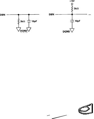
2Serial timing is measured with a 4.7 kΩ pull-up resistor on SDATA and SSTRB and a 2 kΩ pull-up on SCLK. The capacitance on all three outputs is 35 pF. 3t6 is measured with the load circuits of Figure 1 and defined as the time required for an output to cross 0.8 V or 2.4 V.
4t7 is defined as the time required for the data lines to change 0.5 V when loaded with the circuits of Figure 2. 5SCLK mark/space ratio (measured from a voltage level of 1.6 V) is 40/60 to 60/40.
6SDATA will drive higher capacitive loads but this will add to t12 since it increases the external RC time constant (4.7 kΩiCL) and hence the time to reach 2.4 V. Specifications subject to chance without notice.
ABSOLUTE MAXIMUM RATINGS* |
|
|
VDD to AGND . . . . . . . . . . . . . . . . . . . . . |
. . |
. . . –0.3 V to +7 V |
VSS to AGND . . . . . . . . . . . . . . . . . . . . . |
. . |
. . . +0.3 V to –7 V |
AGND to DGND . . . . . . . . . . . . . . . . . |
–0.3 V to VDD +0.3 V |
|
VIN to AGND . . . . . . . . . . . . . . . . . . . . . |
. . . |
. –15 V to +15 V |
REF OUT to AGND . . . . . . . . . . . . . . . . |
. . . |
. . . . . 0 V to VDD |
Digital Inputs to DGND . . . . . . . . . . . . |
–0.3 V to VDD +0.3 V |
|
Digital Outputs to DGND . . . . . . . . . . . |
–0.3 V to VDD +0.3 V |
|
Operating Temperature Range |
|
. . . 0°C to +70°C |
Commercial (J, K, L Versions – AD7870) |
||
Commercial (K, L Versions – AD7875) |
. . . |
. . 0°C to +70°C |
Industrial (A, B, C Versions – AD7870) |
. . . |
.–25°C to +85°C |
Industrial (B, C Versions – AD7875/AD7876) |
||
. . . . . . . . . . . . . . . . . . . . . . . . . . . . . . . |
. . . |
.–40°C to +85°C |
Extended (S, T Versions) . . . . . . . . . . . |
. . . |
–55°C to +125°C |
Storage Temperature Range . . . . . . . . . . |
. . . |
–65°C to +150°C |
Lead Temperature (Soldering, 10 sec) . . . |
. . . |
. . . . . . . +300°C |
Power Dissipation (Any Package) to +75°C . . |
. . . . . . .450 mW |
|
Derates above +75°C by . . . . . . . . . . . . . |
. . . |
. . . . . 10 mW/°C |
*Stresses above those listed under “Absolute Maximum Ratings” may cause permanent damage to the device. This is a stress rating only; functional operation of the device at these or any other conditions above those listed in the operational sections of this specification is not implied. Exposure to absolute maximum rating conditions for extended periods may affect device reliability.
a. High-Z to VOH b. High-Z to VOL Figure 1. Load Circuits for Access Time
a. VOH to High-Z |
b. VOL to High-Z |
Figure 2. Load Circuits for Output Float Delay
CAUTION |
|
|
|
|
ESD (electrostatic discharge) sensitive device. Electrostatic charges as high as 4000 V readily |
|
WARNING! |
|
|
|
|
|
||
accumulate on the human body and test equipment and can discharge without detection. Although |
|
|
|
|
the AD7870/AD7875/AD7876 feature proprietary ESD protection circuitry, permanent damage |
|
|
|
|
may occur on devices subjected to high energy electrostatic discharges. Therefore, proper ESD |
|
ESD SENSITIVE DEVICE |
|
|
precautions are recommended to avoid performance degradation or loss of functionality. |
|
|
||
|
|
|
||
|
|
|
|
|
–4– |
REV. B |

AD7870/AD7875/AD7876
AD7870 ORDERING GUIDE
|
Temperature |
VIN Voltage |
|
Integral |
|
Model1, 2 |
SNR |
Nonlinearity |
Package |
||
Range |
Range (V) |
(dBs) |
(LSB) |
Option3 |
|
AD7870JN |
0°C to +70°C |
±3 |
70 min |
±1/2 typ |
N-24 |
AD7870KN |
0°C to +70°C |
±3 |
70 min |
±1 max |
N-24 |
AD7870LN |
0°C to +70°C |
±3 |
72 min |
±1/2 max |
N-24 |
AD7870JP |
0°C to +70°C |
±3 |
70 min |
±1/2 typ |
P-28A |
AD7870KP |
0°C to +70°C |
±3 |
70 min |
±1 max |
P-28A |
AD7870LP |
0°C to +70°C |
±3 |
72 min |
±1/2 max |
P-28A |
AD7870AQ |
–25°C to +85°C |
±3 |
70 min |
±1/2 typ |
Q-24 |
AD7870BQ |
–25°C to +85°C |
±3 |
70 min |
±1 max |
Q-24 |
AD7870CQ |
–25°C to +85°C |
±3 |
72 min |
±1/2 max |
Q-24 |
AD7870SQ4 |
–55°C to +125°C |
±3 |
70 min |
±1/2 typ |
Q-24 |
AD7870TQ4 |
–55°C to +125°C |
±3 |
70 min |
±1 max |
Q-24 |
NOTES
1To order MIL-STD-883, Class B, processed parts, add /883B to part number. Contact local sales office for military data sheet. 2Contact local sales office for LCCC (Leadless Ceramic Chip Carrier) availability.
3N = Narrow Plastic DIP; P = Plastic Leaded Chip Carrier (PLCC); Q = Cerdip. 4Available to /883B processing only.
AD7875 ORDERING GUIDE
|
|
|
|
Integral |
|
|
Temperature |
VIN Voltage |
SNR |
Nonlinearity |
Package |
Model1, 2 |
Range |
Range (V) |
(dBs) |
(LSB) |
Option3 |
AD7875KN |
0°C to +70°C |
0 to +5 |
70 min |
±1 max |
N-24 |
AD7875LN |
0°C to +70°C |
0 to +5 |
72 min |
±1/2 max |
N-24 |
AD7875KP |
0°C to +70°C |
0 to +5 |
70 min |
±1 max |
P-28A |
AD7875LP |
0°C to +70°C |
0 to +5 |
72 min |
±1/2 max |
P-28A |
AD7875BQ |
–40°C to +85°C |
0 to +5 |
70 min |
±1 max |
Q-24 |
AD7875CQ |
–40°C to +85°C |
0 to +5 |
72 min |
±1/2 max |
Q-24 |
AD7875TQ4 |
–55°C to +125°C |
0 to +5 |
70 min |
±1 max |
Q-24 |
NOTES
1To order MIL-STD-883, Class B. processed parts, add /883B to part number. Contact local sales office for military data sheet. 2Contact local sales office for LCCC (Leadless Ceramic Chip Carrier) availability.
3N = Narrow Plastic DlP; P = Plastic Leaded Chip Carrier (PLCC); Q = Cerdip. 4Available to /883B processing only.
AD7876 ORDERING GUIDE
|
Temperature |
VIN Voltage |
Integral |
|
Model1 |
Nonlinearity |
Package |
||
Range |
Range (V) |
(LSB) |
Option2 |
|
AD7876BN |
–40°C to +85°C |
±10 |
±1 max |
N-24 |
AD7876CN |
–40°C to +85°C |
±10 |
±1/2 max |
N-24 |
AD7876BR |
–40°C to +85°C |
±10 |
±1 max |
R-24 |
AD7876CR |
–40°C to +85°C |
±10 |
±1/2 max |
R-24 |
AD7876BQ |
–40°C to +85°C |
±10 |
±1 max |
Q-24 |
AD7876CQ |
–40°C to +85°C |
±10 |
±1/2 max |
Q-24 |
AD7876TQ3 |
–55°C to +125°C |
±10 |
±1 max |
Q-24 |
NOTES
1To order MIL-STD-883, Class B, processed parts, add /883B to the part number. Contact local sales office for military data sheet. 2N = Narrow Plastic DIP; Q = Cerdip; R = Small Outline IC (SOIC).
3Available to /883B processing only.
REV. B |
–5– |
AD7870/AD7875/AD7876
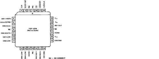
PIN FUNCTION DESCRIPTION
DIP |
|
Pin |
|
|
|
|
|
|
|
|
|
|
|
|
|
|
|
|
|
|
|
|
|
|
|
|
|
|
|
|
|
|
|
|
|
|
|
|
|
|
|||||||||
Pin No. |
|
Mnemonic |
|
Function |
|
|
|
|
|
|
|
|
|
|
|
|
|
|
|
|
|
|
|
|
|
|
|
|
|
|
|
|
|
|
|||||||||||||||
|
|
|
|
|
|
|
|
|
|
|
|
|
|
|
|
|
|
|
|
|
|
|
|
|
|
|
|
|
|
|
|
|
|
|
|
|
|
|
|
|
|
|
|
|
|
|
|
||
1 |
|
|
|
|
|
|
|
|
|
|
|
|
|
|
Read. Active low logic input. This input is used in conjunction with |
|
low to enable the data outputs. |
||||||||||||||||||||||||||||||||
RD |
|
|
|
CS |
|||||||||||||||||||||||||||||||||||||||||||||
2 |
|
|
|
|
|
/ |
|
|
|
|
|
Busy/Interrupt, Active low logic output indicating converter status. See timing diagrams. |
|
|
|
|
|
|
|
|
|
|
|||||||||||||||||||||||||||
BUSY |
INT |
|
|
|
|
|
|
|
|
|
|
||||||||||||||||||||||||||||||||||||||
3 |
|
CLK |
|
|
|
Clock input. An external TTL-compatible clock may be applied to this input pin. Alternatively, tying this pin to |
|||||||||||||||||||||||||||||||||||||||||||
|
|
|
|
|
|
|
|
|
|
|
|
|
|
|
VSS enables the internal laser-trimmed clock oscillator. |
|
|
|
|
|
|
|
|
|
|
|
|
|
|
|
|
|
|||||||||||||||||
4 |
|
DB11/HBEN |
|
Data Bit 11 (MSB)/High Byte Enable. The function of this pin is dependent on the state of the 12/ |
8 |
/CLK input (see |
|||||||||||||||||||||||||||||||||||||||||||
|
|
|
|
|
|
|
|
|
|
|
|
|
|
|
below). When 12-bit parallel data is selected, this pin provides the DB11 output. When byte data is selected, this pin |
||||||||||||||||||||||||||||||||||
|
|
|
|
|
|
|
|
|
|
|
|
|
|
|
becomes the HBEN logic input HBEN is used for 8-bit bus interfacing. When HBEN is low, DB7/LOW to DB0/DB8 |
||||||||||||||||||||||||||||||||||
|
|
|
|
|
|
|
|
|
|
|
|
|
|
|
become DB7 to DB0. With HBEN high, DB7/LOW to DB0/DB8 are used for the upper byte of data (see Table I). |
||||||||||||||||||||||||||||||||||
5 |
|
DB10/ |
|
|
|
|
Data Bit 10/Serial Strobe. When 12-bit parallel data is selected, this pin provides the DB10 output. |
|
|
|
is an |
||||||||||||||||||||||||||||||||||||||
SSTRB |
SSTRB |
||||||||||||||||||||||||||||||||||||||||||||||||
|
|
|
|
|
|
|
|
|
|
|
|
|
|
|
active low open-drain output that provides a strobe or framing pulse for serial data. An external 4.7 kΩ pull-up |
||||||||||||||||||||||||||||||||||
|
|
|
|
|
|
|
|
|
|
|
|
|
|
|
resistor is required on SSTRB. |
|
|
|
|
|
|
|
|
|
|
|
|
|
|
|
|
|
|
|
|
|
|
|
|
|
|
|
|||||||
6 |
|
DB9/SCLK |
|
Data Bit 9/Serial Clock. When 12-bit parallel data is selected, this pin provides the DB9 output. SCLK is the gated |
|||||||||||||||||||||||||||||||||||||||||||||
|
|
|
|
|
|
|
|
|
|
|
|
|
|
|
serial clock output derived from the internal or external ADC clock. If the 12/8/CLK input is at –5 V, then SCLK |
||||||||||||||||||||||||||||||||||
|
|
|
|
|
|
|
|
|
|
|
|
|
|
|
runs continuously. If 12/8/CLK is at 0 V, then SCLK is gated off after serial transmission is complete. SCLK is an |
||||||||||||||||||||||||||||||||||
|
|
|
|
|
|
|
|
|
|
|
|
|
|
|
open-drain output and requires an external 2 kΩ pull-up resistor. |
|
|
|
|
|
|
|
|
|
|
|
|
|
|
||||||||||||||||||||
7 |
|
DB8/SDATA |
|
Data Bit 8/Serial Data. When 12-bit parallel data is selected, this pin provides the DB8 output. SDATA is an open- |
|||||||||||||||||||||||||||||||||||||||||||||
|
|
|
|
|
|
|
|
|
|
|
|
|
|
|
drain serial data output which is used with SCLK and SSTRB for serial data transfer. Serial data is valid on the fall- |
||||||||||||||||||||||||||||||||||
|
|
|
|
|
|
|
|
|
|
|
|
|
|
|
ing edge of SCLK while SSTRB is low. An external 4.7 kΩ pull-up resistor is required on SDATA. |
||||||||||||||||||||||||||||||||||
8–11 |
|
DB7/LOW– |
|
Three-state data outputs controlled by |
CS |
and |
RD |
. Their function depends on the 12/ |
8 |
/CLK and HBEN inputs. |
|||||||||||||||||||||||||||||||||||||||
|
|
DB4/LOW |
|
|
|
With 12/8/CLK high, they are always DB7–DB4. With 12/8/CLK low or –5 V, their function is controlled by HBEN |
|||||||||||||||||||||||||||||||||||||||||||
|
|
|
|
|
|
|
|
|
|
|
|
|
|
|
(see Table I). |
|
|
|
|
|
|
|
|
|
|
|
|
|
|
|
|
|
|
|
|
|
|
|
|
|
|
|
|
|
|
||||
12 |
|
DGND |
|
|
|
Digital Ground. Ground reference for digital circuitry. |
|
|
|
|
|
|
|
|
|
|
|
|
|
|
|
|
|
||||||||||||||||||||||||||
13–16 |
|
DB3/DB11– |
|
Three-state data outputs which are controlled by |
|
and |
|
. Their function depends on the 12/ |
|
/CLK and HBEN |
|||||||||||||||||||||||||||||||||||||||
CS |
RD |
8 |
|||||||||||||||||||||||||||||||||||||||||||||||
|
|
DB0/DB8 |
|
|
|
inputs. With 12/ |
8 |
/CLK high, they are always DB3–DB0. With 12/8/CLK low or –5 V, their function is controlled by |
|||||||||||||||||||||||||||||||||||||||||
|
|
|
|
|
|
|
|
|
|
|
|
|
|
|
HBEN (see Table I). |
|
|
|
|
|
|
|
|
|
|
|
|
|
|
|
|
|
|
|
|
|
|
|
|
|
|
|
|
|
|
||||
|
|
|
|
|
|
|
|
|
|
|
|
|
|
|
|
|
|
|
|
Table I. Output Data for Byte Interfacing |
|
|
|
|
|
|
|
|
|
|
|
|
|
|
|||||||||||||||
|
|
|
|
|
|
|
|
|
|
|
|
|
|
|
|
|
|||||||||||||||||||||||||||||||||
|
|
HBEN |
|
DB7/LOW |
DB6/LOW |
|
DB5/LOW |
DB4/LOW |
|
DB3/DB11 |
DB2/DB10 |
DB1/DB9 |
DB0/DB8 |
|
|||||||||||||||||||||||||||||||||||
|
|
HIGH |
|
LOW |
LOW |
|
LOW |
LOW |
|
DB11(MSB) |
DB10 |
DB9 |
DB8 |
|
|
||||||||||||||||||||||||||||||||||
|
|
LOW |
|
DB7 |
|
DB6 |
|
DB5 |
DB4 |
|
DB3 |
DB2 |
DB1 |
DB0 (LSB) |
|
||||||||||||||||||||||||||||||||||
17 |
|
VDD |
|
|
|
Positive Supply, +5 V ± 5%. |
|
|
|
|
|
|
|
|
|
|
|
|
|
|
|
|
|
|
|
|
|
|
|
|
|
|
|
||||||||||||||||
18 |
|
AGND |
|
|
|
Analog Ground. Ground reference for track/hold, reference and DAC. |
|
|
|
|
|
|
|
|
|
|
|
|
|
|
|||||||||||||||||||||||||||||
19 |
|
REF OUT |
|
|
|
Voltage Reference Output. The internal 3 V reference is provided at this pin. The external load capability is 500 μA. |
|||||||||||||||||||||||||||||||||||||||||||
20 |
|
VIN |
|
|
|
Analog Input. The analog input range is ±3 V for the AD7870, ±10 V for the AD7876 and 0 V to +5 V for the AD7875. |
|||||||||||||||||||||||||||||||||||||||||||
21 |
|
VSS |
|
|
|
Negative Supply, –5 V ± 5%. |
|
|
|
|
|
|
|
|
|
|
|
|
|
|
|
|
|
|
|
|
|
|
|
|
|
|
|
||||||||||||||||
22 |
|
12/ |
8 |
/CLK |
|
|
|
Three Function Input. Defines the data format and serial clock format. With this pin at +5 V, the output data for- |
|||||||||||||||||||||||||||||||||||||||||
|
|
|
|
|
|
|
|
|
|
|
|
|
|
|
mat is 12-bit parallel only. With this pin at 0 V, either byte or serial data is available and SCLK is not continuous. |
||||||||||||||||||||||||||||||||||
|
|
|
|
|
|
|
|
|
|
|
|
|
|
|
With this pin at –5 V, either byte or serial data is again available but SCLK is now continuous. |
||||||||||||||||||||||||||||||||||
23 |
|
|
|
|
|
|
|
|
Convert Start. A low to high transition on this input puts the track/hold into its hold mode and starts conversion. |
||||||||||||||||||||||||||||||||||||||||
CONVST |
|
|
|
||||||||||||||||||||||||||||||||||||||||||||||
|
|
|
|
|
|
|
|
|
|
|
|
|
|
|
This input is asynchronous to the CLK input. |
|
|
|
|
|
|
|
|
|
|
|
|
|
|
|
|
|
|
|
|
|
|
|
|||||||||||
24 |
|
|
|
|
|
|
|
Chip Select. Active low logic input. The device is selected when this input is active. With |
|
|
tied low, a new |
||||||||||||||||||||||||||||||||||||||
CS |
|
|
|
CONVST |
|||||||||||||||||||||||||||||||||||||||||||||
|
|
|
|
|
|
|
|
|
|
|
|
|
|
|
conversion is initiated when |
CS |
goes low. |
|
|
|
|
|
|
|
|
|
|
|
|
|
|
|
|
|
|
|
|
|
|
|
|||||||||
|
|
|
|
|
|
|
|
|
|
|
|
|
|
|
DIP and SOIC2 |
|
|
PIN CONFIGURATIONS1 |
|
|
|
PLCC2 |
|
|
|
|
|
|
|
|
|
|
|||||||||||||||||
|
|
|
|
|
|
|
|
|
|
|
|
|
|
|
|
|
|
|
|
|
|
|
|
|
|
|
|
|
|
|
|
|
|
|
|
|
|
|
|
|
|||||||||
1PIN CONFIGURATIONS ARE THE SAME FOR THE AD7875 AND AD7876.
2THE AD7870 AND AD7875 ARE AVAILABLE IN DIP AND PLCC; THE AD7870A IS AVAILABLE IN PLASTIC DIP; THE AD7875 AND AD7876 ARE AVAILABLE IN SOIC AND DIP.
–6– |
REV. B |
Loading...