


 Loading...
Analog Devices AD829SQ-883B, AD829SQ, AD829SE-883B, AD829SCHIPS, AD829JR-REEL7 Datasheet
...a |
High-Speed, Low-Noise |
Video Op Amp |
FEATURES
High Speed
120 MHz Bandwidth, Gain = –1
230 V/ s Slew Rate
90 ns Settling Time to 0.1% Ideal for Video Applications
0.02% Differential Gain
0.04 Differential Phase
Low Noise
1.7 nV/√Hz Input Voltage Noise
1.5 pA/√Hz Input Current Noise Excellent DC Precision
1 mV max Input Offset Voltage (Over Temp)
0.3 V/ C Input Offset Drift
Flexible Operation
Specified for 5 V to 15 V Operation3 V Output Swing into a 150 Load
External Compensation for Gains 1 to 20 5 mA Supply Current
Available in Tape and Reel in Accordance with EIA-481A Standard
PRODUCT DESCRIPTION
The AD829 is a low noise (1.7 nV/√Hz), high speed op amp with custom compensation that provides the user with gains from ±1 to ±20 while maintaining a bandwidth greater than 50 MHz. The AD829’s 0.04° differential phase and 0.02% differential gain performance at 3.58 MHz and 4.43 MHz,
driving reverse-terminated 50 Ω or 75 Ω cables, makes it ideally suited for professional video applications. The AD829 achieves its 230 V/µs uncompensated slew rate and 750 MHz gain bandwidth product while requiring only 5 mA of current from the power supplies.
The AD829’s external compensation pin gives it exceptional versatility. For example, compensation can be selected to optimize the bandwidth for a given load and power supply voltage. As a gain-of-two line driver, the –3 dB bandwidth can be increased to 95 MHz at the expense of 1 dB of peaking. In addition, the AD829’s output can also be clamped at its external compensation pin.
The AD829 has excellent dc performance. It offers a minimum open-loop gain of 30 V/mV into loads as low as 500 Ω, low input voltage noise of 1.7 nV/√Hz, and a low input offset voltage of 1 mV maximum. Common-mode rejection and power supply rejection ratios are both 120 dB.
The AD829 is also useful in multichannel, high speed data conversion where its fast (90 ns to 0.1%) settling time is of importance. In such applications, the AD829 serves as an input buffer for 8-to-10-bit A/D converters and as an output I/V converter for high speed D/A converters.
REV. E
Information furnished by Analog Devices is believed to be accurate and reliable. However, no responsibility is assumed by Analog Devices for its use, nor for any infringements of patents or other rights of third parties which may result from its use. No license is granted by implication or otherwise under any patent or patent rights of Analog Devices.
AD829
CONNECTION DIAGRAMS
8-Lead Plastic Mini-DIP (N),
Cerdip (Q) and SOIC (R) Packages
OFFSET NULL |
1 |
AD829 |
8 |
OFFSET NULL |
–IN |
2 |
|
7 |
+VS |
+IN |
3 |
|
6 |
OUTPUT |
–VS |
4 |
TOP VIEW |
5 |
CCOMP |
|
|
(Not to Scale) |
|
|
20-Lead LCC Pinout
|
NC OFFSET NULL |
NC |
OFFSET NULL |
NC |
|
|
|
3 |
2 |
1 |
20 19 |
|
|
NC 4 |
|
|
|
|
|
18 NC |
|
|
|
|
|
||
|
|
|
|
|
||
|
|
|
|
|
||
|
|
|
|
|
||
–IN 5 |
|
AD829 |
|
17 +V |
||
NC 6 |
|
|
16 NC |
|||
|
TOP VIEW |
|
||||
+IN 7 |
(Not to Scale) |
15 OUTPUT |
||||
NC 8 |
|
|
|
|
|
14 NC |
|
|
|
|
|
|
|
|
9 |
10 |
11 12 |
13 |
|
|
|
NC |
–V |
NC |
COMP |
NC |
|
NC = NO CONNECT |
|
C |
|
|
||
The AD829 provides many of the same advantages that a transimpedance amplifier offers, while operating as a traditional voltage feedback amplifier. A bandwidth greater than 50 MHz can be maintained for a range of gains by changing the external compensation capacitor. The AD829 and the transimpedance amplifier are both unity gain stable and provide similar voltage noise performance (1.7 nV/√Hz). However, the current noise of the AD829 (1.5 pA/√Hz) is less than 10% of the noise of transimpedance amps. Furthermore, the inputs of the AD829 are symmetrical.
PRODUCT HIGHLIGHTS
1.Input voltage noise of 2 nV/√Hz, current noise of 1.5 pA/ √Hz and 50 MHz bandwidth, for gains of 1 to 20, make the AD829 an ideal preamp.
2.Differential phase error of 0.04° and a 0.02% differential gain error, at the 3.58 MHz NTSC and 4.43 MHz PAL and
SECAM color subcarrier frequencies, make it an outstanding video performer for driving reverse-terminated 50 Ω and
75 Ω cables to ±1 V (at their terminated end).
3.The AD829 can drive heavy capacitive loads.
4. Performance is fully specified for operation from ±5 V to
±15 V supplies.
5.Available in plastic, cerdip, and small outline packages. Chips and MIL-STD-883B parts are also available.
One Technology Way, P.O. Box 9106, Norwood, MA 02062-9106, U.S.A.
Tel: 781/329-4700 |
World Wide Web Site: http://www.analog.com |
Fax: 781/326-8703 |
© Analog Devices, Inc., 2000 |
AD829–SPECIFICATIONS (@ TA = +25 C and VS = 15 V dc, unless otherwise noted)
|
|
|
|
AD829J/AR |
|
AD829AQ/S |
|
|
|
Model |
Conditions |
VS |
Min |
Typ |
Max |
Min |
Typ |
Max |
Units |
INPUT OFFSET VOLTAGE |
|
±5 V, ±15 V |
|
0.2 |
1 |
|
0.1 |
0.5 |
mV |
|
TMIN to TMAX |
±5 V, ±15 V |
|
|
1 |
|
|
0.5 |
mV |
Offset Voltage Drift |
|
|
0.3 |
|
|
0.3 |
|
µV/°C |
|
|
|
|
|
|
|
|
|
|
|
INPUT BIAS CURRENT |
|
±5 V, ±15 V |
|
3.3 |
7 |
|
3.3 |
7 |
µA |
|
TMIN to TMAX |
|
|
|
8.2/9.5 |
|
|
9.5 |
µA |
INPUT OFFSET CURRENT |
|
±5 V, ±15 V |
|
50 |
500 |
|
50 |
500 |
nA |
|
TMIN to TMAX |
±5 V, ±15 V |
|
|
500 |
|
|
500 |
nA |
Offset Current Drift |
|
|
0.5 |
|
|
0.5 |
|
nA/°C |
|
|
|
|
|
|
|
|
|
|
|
OPEN-LOOP GAIN |
VO = ±2.5 V |
±5 V |
|
|
|
|
|
|
|
|
RLOAD = 500 Ω |
|
30 |
65 |
|
30 |
65 |
|
V/mV |
|
TMIN to TMAX |
|
20 |
|
|
20 |
|
|
V/mV |
|
RLOAD = 150 Ω |
|
|
40 |
|
|
40 |
|
V/mV |
|
VOUT = ±10 V |
±15 V |
|
|
|
|
|
|
|
|
RLOAD = 1 kΩ |
|
50 |
100 |
|
50 |
100 |
|
V/mV |
|
TMIN to TMAX |
|
20 |
|
|
20 |
|
|
V/mV |
|
RLOAD = 500 Ω |
|
|
85 |
|
|
85 |
|
V/mV |
DYNAMIC PERFORMANCE |
|
±5 V |
|
|
|
|
|
|
|
Gain Bandwidth Product |
|
|
600 |
|
|
600 |
|
MHz |
|
Full Power Bandwidth1, 2 |
|
±15 V |
|
750 |
|
|
750 |
|
MHz |
VO = 2 V p-p |
|
|
|
|
|
|
|
|
|
|
RLOAD = 500 Ω |
±5 V |
|
25 |
|
|
25 |
|
MHz |
|
VO = 20 V p-p |
|
|
|
|
|
|
|
|
|
RLOAD = 1 kΩ |
±15 V |
|
3.6 |
|
|
3.6 |
|
MHz |
Slew Rate2 |
RLOAD = 500 Ω |
±5 V |
|
150 |
|
|
150 |
|
V/µs |
|
RLOAD = 1 kΩ |
±15 V |
|
230 |
|
|
230 |
|
V/µs |
Settling Time to 0.1% |
AV = –19 |
±5 V |
|
|
|
|
|
|
|
|
–2.5 V to +2.5 V |
|
65 |
|
|
65 |
|
ns |
|
|
10 V Step |
±15 V |
|
90 |
|
|
90 |
|
ns |
Phase Margin2 |
CLOAD = 10 pF |
±15 V |
|
|
|
|
|
|
|
|
RLOAD = 1 kΩ |
|
|
60 |
|
|
60 |
|
Degrees |
DIFFERENTIAL GAIN ERROR3 |
RLOAD = 100 Ω |
±15 V |
|
|
|
|
|
|
|
|
CCOMP = 30 pF |
|
|
0.02 |
|
|
0.02 |
|
% |
DIFFERENTIAL PHASE ERROR3 |
RLOAD = 100 Ω |
±15 V |
|
|
|
|
|
|
|
|
CCOMP = 30 pF |
|
|
0.04 |
|
|
0.04 |
|
Degrees |
COMMON-MODE REJECTION |
VCM = ± 2.5 V |
±5 V |
100 |
120 |
|
100 |
120 |
|
dB |
|
VCM = ± 12 V |
±15 V |
100 |
120 |
|
100 |
120 |
|
dB |
|
TMIN to TMAX |
|
96 |
|
|
96 |
|
|
dB |
POWER SUPPLY REJECTION |
VS = ±4.5 V to ±18 V |
|
98 |
120 |
|
98 |
120 |
|
dB |
|
TMIN to TMAX |
|
94 |
|
|
94 |
|
|
dB |
INPUT VOLTAGE NOISE |
f = 1 kHz |
±15 V |
|
1.7 |
2 |
|
1.7 |
2 |
nV/√Hz |
|
|
|
|
|
|
|
|
|
|
INPUT CURRENT NOISE |
f = 1 kHz |
±15 V |
|
1.5 |
|
|
1.5 |
|
pA/√Hz |
|
|
|
|
|
|
|
|
|
|
INPUT COMMON-MODE |
|
±5 V |
|
|
|
|
|
|
|
VOLTAGE RANGE |
|
|
+4.3 |
|
|
+4.3 |
|
V |
|
|
|
±15 V |
|
–3.8 |
|
|
–3.8 |
|
V |
|
|
|
+14.3 |
|
|
+14.3 |
|
V |
|
|
|
|
|
–13.8 |
|
|
–13.8 |
|
V |
|
|
|
|
|
|
|
|
|
|
OUTPUT VOLTAGE SWING |
RLOAD = 500 Ω |
±5 V |
3.0 |
3.6 |
|
3.0 |
3.6 |
|
±V |
|
RLOAD = 150 Ω |
±5 V |
2.5 |
3.0 |
|
2.5 |
3.0 |
|
±V |
|
RLOAD = 50 Ω |
±5 V |
|
1.4 |
|
|
1.4 |
|
±V |
|
RLOAD = 1 kΩ |
±15 V |
12 |
13.3 |
|
12 |
13.3 |
|
±V |
|
RLOAD = 500 Ω |
±15 V |
10 |
12.2 |
|
10 |
12.2 |
|
±V |
Short Circuit Current |
|
±5 V, ±15 V |
|
32 |
|
|
32 |
|
mA |
INPUT CHARACTERISTICS |
|
|
|
|
|
|
|
|
kΩ |
Input Resistance (Differential) |
|
|
|
13 |
|
|
13 |
|
|
Input Capacitance (Differential)4 |
|
|
|
5 |
|
|
5 |
|
pF |
Input Capacitance (Common Mode) |
|
|
|
1.5 |
|
|
1.5 |
|
pF |
|
|
|
|
|
|
|
|
|
|
CLOSED-LOOP OUTPUT |
|
|
|
|
|
|
|
|
mΩ |
RESISTANCE |
AV = +1, f = 1 kHz |
|
|
2 |
|
|
2 |
|
|
–2– |
REV. E |
|
|
|
|
|
|
|
|
AD829 |
|
|
|
AD829J/AR |
|
|
AD829AQ/S |
|
|
Model |
Conditions |
VS |
Min Typ |
Max |
Min |
Typ |
Max |
Units |
POWER SUPPLY |
|
|
±4.5 |
±18 |
±4.5 |
|
±18 |
|
Operating Range |
|
±5 V |
|
V |
||||
Quiescent Current |
|
5 |
6.5 |
|
5 |
6.5 |
mA |
|
|
TMIN to TMAX |
±15 V |
|
8.0 |
|
|
8.2/8.7 |
mA |
|
|
5.3 |
6.8 |
|
5.3 |
6.8 |
mA |
|
|
TMIN to TMAX |
|
|
8.3/8.5 |
|
|
8.5/9.0 |
mA |
TRANSISTOR COUNT |
Number of Transistors |
|
46 |
|
|
46 |
|
|
|
|
|
|
|
|
|
|
|
NOTES
1Full Power Bandwidth = Slew Rate/2 π VPEAK. 2Tested at Gain = +20, CCOMP = 0 pF.
33.58 MHz (NTSC) and 4.43 MHz (PAL & SECAM).
4Differential input capacitance consists of 1.5 pF package capacitance plus 3.5 pF from the input differential pair.
Specifications subject to change without notice.
ABSOLUTE MAXIMUM RATINGS1
Supply Voltage . . . . . . . . . . . . . . . . . . . . . . . . . . . . . . . . ±18 V Internal Power Dissipations2
Plastic (N) . . . . . . . . . . . . . . . . . . . . . . . . . . . . . . 1.3 Watts Small Outline (R) . . . . . . . . . . . . . . . . . . . . . . . . . 0.9 Watts Cerdip (Q) . . . . . . . . . . . . . . . . . . . . . . . . . . . . . . 1.3 Watts LCC (E) . . . . . . . . . . . . . . . . . . . . . . . . . . . . . . . 0.8 Watts
Input Voltage . . . . . . . . . . . . . . . . . . . . . . . . . . . . . . . . . . . ±VS Differential Input Voltage3 . . . . . . . . . . . . . . . . . . . . ±6 Volts
Output Short Circuit Duration . . . . . . . . . . . . . . . . Indefinite Storage Temperature Range (Q, E) . . . . . . . –65°C to +150°C Storage Temperature Range (N, R) . . . . . . . –65°C to +125°C Operating Temperature Range
AD829J . . . . . . . . . . . . . . . . . . . . . . . . . . . . . 0°C to +70°C AD829A . . . . . . . . . . . . . . . . . . . . . . . . . . . –40°C to +85°C AD829S . . . . . . . . . . . . . . . . . . . . . . . . . . –55°C to +125°C Lead Temperature Range (Soldering 60 sec) . . . . . . . .+300°C
NOTES
1Stresses above those listed under Absolute Maximum Ratings may cause permanent damage to the device. This is a stress rating only and functional operation of the device at these or any other conditions above those indicated in the operational section of this specification is not implied. Exposure to absolute maximum rating conditions for extended periods may affect device reliability.
2Maximum internal power dissipation is specified so that TJ does not exceed +175°C at an ambient temperature of +25°C.
Thermal characteristics:
8-lead plastic package: θJA = 100°C/watt (derate at 8.7 mW/°C) 8-lead cerdip package: θJA = 110°C/watt (derate at 8.7 mW/°C) 20-lead LCC package: θJA = 150°C/watt
8-lead small outline package: θJA = 155°C/watt (derate at 6 mW/°C).
3If the differential voltage exceeds 6 volts, external series protection resistors should be added to limit the input current.
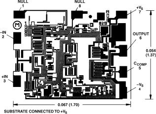
METALIZATION PHOTO
Contact factory for latest dimensions.
Dimensions shown in inches and (mm).
ESD SUSCEPTIBILITY
ESD (electrostatic discharge) sensitive device. Electrostatic charges as high as 4000 volts, which readily accumulate on the human body and on test equipment, can discharge without detection. Although the AD829 features proprietary ESD protection circuitry, permanent damage may still occur on these devices if they are subjected to high energy electrostatic discharges. Therefore, proper ESD precautions are recommended to avoid any performance degradation or loss of functionality.
ORDERING GUIDE
Model |
Temperature Range |
Package Description |
Package Option* |
|
|
|
|
AD829JN |
0°C to +70°C |
8-Lead Plastic Mini-DIP |
N-8 |
AD829AR |
–40°C to +85°C |
8-Lead Plastic SOIC |
SO-8 |
AD829JR |
0°C to +70°C |
8-Lead Plastic SOIC |
SO-8 |
AD829AR-REEL7 |
–40°C to +85°C |
Tape and Reel 7" |
|
AD829AR-REEL |
–40°C to +85°C |
Tape and Reel 13" |
|
AD829JR-REEL7 |
0°C to +70°C |
Tape and Reel 7" |
|
AD829JR-REEL |
0°C to +70°C |
Tape and Reel 13" |
|
AD829AQ |
–40°C to +85°C |
8-Lead Cerdip |
Q-8 |
AD829SQ |
–55°C to +125°C |
8-Lead Cerdip |
Q-8 |
AD829SQ/883B |
–55°C to +125°C |
8-Lead Cerdip |
Q-8 |
5962-9312901MPA |
–55°C to +125°C |
8-Lead Cerdip |
Q-8 |
AD829SE/883B |
–55°C to +125°C |
20-Lead LCC |
E-20A |
5962-9312901M2A |
–55°C to +125°C |
20-Lead LCC |
E-20A |
AD829JCHIPS |
0°C to +70°C |
Die |
|
AD829SCHIPS |
–55°C to +125°C |
Die |
|
|
|
|
|
*E = Leadless Chip Carrier (Ceramic); N = Plastic DIP; Q = Cerdip; SO = Small Outline IC (SOIC).
REV. E |
–3– |

AD829–Typical Performance Characteristics
– Volts |
20 |
|
|
|
|
|
|
|
|
|
|
|
|
|
|
|
|
||
|
|
|
|
|
|
|
|
|
|
RANGE |
15 |
|
|
|
|
|
|
|
|
MODE-COMMON |
|
|
|
+VOUT |
|
|
|
|
|
|
|
|
|
|
|
|
|
||
10 |
|
|
|
|
|
|
|
|
|
|
|
|
|
–VOUT |
|
|
|
|
|
|
|
|
|
|
|
|
|
|
|
INPUT |
5 |
|
|
|
|
|
|
|
|
|
|
|
|
|
|
|
|
||
|
|
|
|
|
|
|
|
|
|
|
0 |
|
|
|
|
|
|
|
|
|
0 |
5 |
10 |
15 |
20 |
||||
SUPPLY VOLTAGE – Volts
Figure 1. Input Common-Mode Range vs. Supply Voltage
MAGNITUDE OF THE OUTPUT
20 |
|
|
|
|
|
30 |
|
|
|
|
|
|
|
|
|
|
|
|
|
|
|
|
|
|
p–p |
25 |
|
15 VOLT |
|
Volts–VOLTAGE |
|
|
|
|
Volts–SWINGVOLTAGE |
|
|
||
|
|
|
|
|
|
SUPPLIES |
|
||
15 |
|
|
|
|
|
|
|
|
|
|
|
|
|
|
|
|
|
|
|
|
|
+VOUT |
|
|
20 |
|
|
|
|
10 |
|
|
|
|
|
15 |
|
|
|
|
|
|
–VOUT |
|
|
|
|
|
|
|
|
|
|
|
|
|
|
|
|
5 |
|
|
|
|
|
10 |
|
|
|
|
|
|
|
OUTPUT |
|
|
|
|
|
|
|
|
RLOAD = 1k |
|
5 |
|
5 VOLT |
|
|
|
|
|
|
|
|
|
|
SUPPLIES |
|
0 |
|
|
|
|
|
0 |
|
|
|
0 |
5 |
10 |
15 |
20 |
|
|
1k |
10k |
|
|
10 |
100 |
|||||||
|
SUPPLY VOLTAGE – Volts |
|
|
||||||
|
|
|
|
LOAD RESISTANCE – |
|
||||
|
|
|
|
|
|
|
|
||
Figure 2. Output Voltage Swing |
Figure 3. Output Voltage Swing |
|
vs. Supply Voltage |
||
vs. Resistive Load |
||
|
mA |
6.0 |
|
|
|
|
|
|
|
|
|
|
|
|
|
|
|
|
|
|
|
|
|
|
|
|
|
|
|
|
|
|
|
|
|
|
|
|
|
|||
5.5 |
|
|
|
|
|
|
|
|
|
|
|
|
|
|
|
|
|
|
|
|
CURRENT – |
|
|
|
|
|
|
|
|
|
|
|
|
|
|
|
|
|
|
|
|
5.0 |
|
|
|
|
|
|
|
|
|
|
|
|
|
|
|
|
|
|
|
|
|
|
|
|
|
|
|
|
|
|
|
|
|
|
|
|
|
|
|||
QUIESCENT |
4.5 |
|
|
|
|
|
|
|
|
|
|
|
|
|
|
|
|
|
|
|
|
|
|
|
|
|
|
|
|
|
|
|
|
|
|
|
|
|
|
|
|
|
4.0 |
|
|
|
|
|
|
|
|
|
|
|
|
|
|
|
|
|
|
|
|
0 |
|
|
5 |
10 |
|
|
|
15 |
|
20 |
|||||||||
|
|
|
|
SUPPLY VOLTAGE – Volts |
|
|
||||||||||||||
|
Figure 4. Quiescent Current vs. |
|||||||||||||||||||
|
Supply Voltage |
|
|
|
|
|
|
|||||||||||||
– mA |
7 |
|
|
|
|
|
|
|
|
|
|
|
|
|
|
|
|
|
|
|
6 |
|
|
|
|
|
|
|
|
|
|
|
|
|
|
|
|
|
|
|
|
CURRENT |
|
|
|
|
|
|
|
VS = 15V |
|
|
|
|
|
|
|
|
||||
5 |
|
|
|
|
|
|
|
|
|
|
|
|
|
|
|
|
|
|
|
|
|
|
|
|
|
|
|
|
|
|
|
|
|
|
|
|
|
|
|
||
QUIESCENT |
|
|
|
|
|
|
|
|
|
|
|
|
|
|
|
|
|
|
|
|
|
|
|
|
|
|
|
VS |
= |
5V |
|
|
|
|
|
|
|||||
4 |
|
|
|
|
|
|
|
|
|
|
|
|
|
|
|
|
|
|
|
|
|
|
|
|
|
|
|
|
|
|
|
|
|
|
|
|
|
|
|
||
|
|
|
|
|
|
|
|
|
|
|
|
|
|
|
|
|
|
|
|
|
|
3 |
|
|
|
|
|
|
|
|
|
|
|
|
|
|
|
|
|
|
|
|
|
|
|
|
0 |
20 40 60 |
80 100 120 140 |
|||||||||||||
|
–60 – 40 –20 |
|||||||||||||||||||
TEMPERATURE – C
Figure 7. Quiescent Current vs. Temperature
A |
–5 |
|
|
|
|
|
|
|
|
|
|
|
|
|
|
|
|
|
|
|
|
|
|
|
|
||
|
|
|
|
|
|
|
|
|
|
|
|
|
|
– |
|
|
|
|
|
|
|
|
|
|
|
|
|
CURRENT |
–4 |
|
|
|
|
|
|
|
|
|
|
|
|
|
|
|
|
|
|
|
|
|
|
|
|
|
|
|
|
|
|
|
|
|
|
|
|
|
|
|
|
BIAS |
|
|
|
|
VS |
= |
5V, 15V |
|
|
|
|
||
–3 |
|
|
|
|
|
|
|
|
|
|
|
|
|
INPUT |
|
|
|
|
|
|
|
|
|
|
|
|
|
|
|
|
|
|
|
|
|
|
|
|
|
|
|
|
–2 |
|
|
|
|
|
|
|
|
|
|
|
|
|
–60 – 40 –20 0 20 40 60 80 100 120 140 |
||||||||||||
|
|
|
|
TEMPERATURE – C |
|||||||||
Figure 5. Input Bias Current vs. Temperature
|
40 |
|
|
|
|
– mA |
|
|
|
NEGATIVE |
|
|
|
|
CURRENT LIMIT |
|
|
LIMIT |
35 |
|
|
|
|
|
|
|
|
|
|
CURRENT |
30 |
|
POSITIVE |
|
|
CURRENT LIMIT |
|
||||
|
|
|
|
|
|
CIRCUIT |
25 |
|
|
VS = 5V |
|
|
|
|
|
|
|
SHORT |
20 |
|
|
|
|
|
|
|
|
|
|
|
15 |
|
|
|
100 120 140 |
|
–60 – 40 –20 |
0 |
20 40 60 80 |
||
|
|
AMBIENT TEMPERATURE – C |
|||
Figure 8. Short Circuit Current Limit vs. Temperature
– |
100 |
|
|
|
|
|
|
|
|
|
|
|
|
IMPEDANCE |
10 |
AV = +20 |
|
|
|
|
|
|
|
|
|||
|
CCOMP = 0pF |
|
|
|||
1 |
|
|
|
|
|
|
OUTPUT |
|
|
|
|
|
|
0.1 |
|
|
|
|
|
|
|
|
|
|
|
|
|
LOOP |
|
|
|
AV = +1 |
|
|
0.01 |
|
|
CCOMP = 68pF |
|
||
- |
|
|
|
|
|
|
CLOSED |
|
|
|
|
|
|
0.001 |
10k |
100k |
1M |
10M |
100M |
|
|
1k |
|||||
|
|
|
FREQUENCY – Hz |
|
|
|
Figure 6. Closed-Loop Output Impedance vs. Frequency
|
65 |
|
|
|
|
|
|
|
VS = ±15V |
|
|
|
|
|
|
|
AV = +20 |
|
|
|
|
|
|
– MHz |
CCOMP = 0pF |
|
|
|
|
||
60 |
|
|
|
|
|
|
|
|
|
|
|
|
|
|
|
dB BANDWIDTH |
55 |
|
|
|
|
|
|
50 |
|
|
|
|
|
|
|
–3 |
|
|
|
|
|
|
|
|
45 |
0 |
20 |
40 |
60 |
80 |
100 120 140 |
|
–60 – 40 –20 |
||||||
|
|
TEMPERATURE – C |
|
||||
Figure 9. –3 dB Bandwidth vs. Temperature
–4– |
REV. E |
Loading...