


Analog Devices AD7945BR, AD7945BN, AD7945ARS-B, AD7945AN-B, AD7943BRS Datasheet
...
a |
+3.3 V/+5 V Multiplying |
|
12-Bit DACs |
||
|
|
|
|
|
AD7943/AD7945/AD7948 |
|
|
|
FEATURES
12-Bit Multiplying DACs
Guaranteed Specifications with +3.3 V/+5 V Supply 0.5 LSBs INL and DNL
Low Power: 5 mW typ
Fast Interface
40 ns Strobe Pulsewidth (AD7943)
40 ns Write Pulsewidth (AD7945, AD7948) Low Glitch: 60 nV-s with Amplifier Connected Fast Settling: 600 ns to 0.01% with AD843
APPLICATIONS
Battery-Powered Instrumentation Laptop Computers
Upgrades for All 754x Series DACs (5 V Designs)
GENERAL DESCRIPTION
The AD7943, AD7945 and AD7948 are fast 12-bit multiplying DACs that operate from a single +5 V supply (Normal Mode) and a single +3.3 V to +5 V supply (Biased Mode). The AD7943 has a serial interface, the AD7945 has a 12-bit parallel interface, and the AD7948 has an 8-bit byte interface. They will replace the industry-standard AD7543, AD7545 and AD7548 in many applications, and they offer superior speed and power consumption performance.
The AD7943 is available in 16-lead DIP, 16-lead SOP (Small Outline Package) and 20-lead SSOP (Shrink Small Outline Package).
The AD7945 is available in 20-lead DIP, 20-lead SOP and 20lead SSOP.
The AD7948 is available in 20-lead DIP, 20-lead SOP and 20lead SSOP.
FUNCTIONAL BLOCK DIAGRAMS
VDD |
|
RFB |
|
|
AD7943 |
|
|
|
IOUT1 |
VREF |
|
12-BIT DAC |
|
|
|
|
IOUT2 |
||
|
|
|
|
|
CLR |
|
DAC REGISTER |
AGND |
|
LD1 |
|
|||
|
|
|||
|
|
|
|
|
LD2 |
|
|
|
|
SRI |
INPUT SHIFT REGISTER |
SRO |
||
STB1 |
STB2 STB3 |
STB4 |
DGND |
|
VDD |
|
RFB |
|
|
AD7945 |
|
|
|
IOUT1 |
VREF |
|
12-BIT DAC |
|
|
|
|
AGND |
||
|
|
|
|
|
|
|
12 |
|
|
CS |
INPUT LATCH |
|
WR |
||
|
|
12 |
|
|
|
DB11–DB0 |
DGND |
|
VDD |
RFB |
|
|
VREF |
12-BIT DAC |
IOUT1 |
|
AGND |
|||
|
|
||
|
12 |
AD7948 |
|
DATA OVERRIDE LOGIC |
DF/DOR |
||
CTRL |
|||
|
|
||
|
12 |
|
|
|
DAC REGISTER |
LDAC |
|
|
12 |
WR |
|
|
|
||
|
INPUT REGISTERS |
CONTROL |
|
|
LOGIC |
||
|
|
||
|
12 |
CSLSB |
|
|
|
||
DATA STEERING LOGIC |
CSMSB |
||
|
8 |
|
|
|
DB7–DB0 |
DGND |
|
REV. B
Information furnished by Analog Devices is believed to be accurate and reliable. However, no responsibility is assumed by Analog Devices for its use, nor for any infringements of patents or other rights of third parties which may result from its use. No license is granted by implication or otherwise under any patent or patent rights of Analog Devices.
One Technology Way, P.O. Box 9106, Norwood, MA 02062-9106, U.S.A.
Tel: 781/329-4700 |
World Wide Web Site: http://www.analog.com |
Fax: 781/326-8703 |
© Analog Devices, Inc., 1998 |
AD7943/AD7945/AD7948–SPECIFICATIONS1
(AD7943: VDD = +4.5 V to +5.5 V; VIOUT1 = VIOUT2 = AGND = 0 V; VREF = +10 V; TA = TMIN to TMAX, unless otherwise noted. AD7945, AD7948: VDD = +4.5 V to +5.5 V; VIOUT1 = AGND = 0 V; VREF = +10 V; TA = TMIN to TMAX, unless otherwise noted.)
Parameter |
B Grades2 |
T Grade2, 3 |
Units |
Test Conditions/Comments |
ACCURACY |
|
|
|
1 LSB = VREF/212 = 2.44 mV when VREF = 10 V |
Resolution |
12 |
12 |
Bits |
|
Relative Accuracy |
±0.5 |
±0.5 |
LSB max |
|
Differential Nonlinearity |
±0.5 |
±0.5 |
LSB max |
All Grades Guaranteed Monotonic over |
|
|
|
|
Temperature |
Gain Error |
±2 |
±2 |
|
|
TMIN to TMAX |
LSB max |
|
||
Gain Temperature Coefficient4 |
2 |
2 |
ppm FSR/°C typ |
|
|
5 |
5 |
ppm FSR/°C max |
|
Output Leakage Current |
|
|
|
|
IOUT1 |
|
|
|
|
@ +25°C |
10 |
10 |
nA max |
See Terminology Section |
TMIN to TMAX |
100 |
100 |
nA max |
Typically 20 nA over Temperature |
REFERENCE INPUT |
|
|
kΩ min |
Typical Input Resistance = 9 kΩ |
Input Resistance |
6 |
6 |
||
|
12 |
12 |
kΩ max |
|
DIGITAL INPUTS |
|
|
|
|
VINH, Input High Voltage |
2.4 |
2.4 |
V min |
|
VINL, Input Low Voltage |
0.8 |
0.8 |
V max |
|
IINH, Input Current |
±1 |
±1 |
μA max |
|
CIN, Input Capacitance4 |
10 |
10 |
pF max |
|
DIGITAL OUTPUT (AD7943 SRO) |
|
|
|
For 1 CMOS Load |
Output Low Voltage (VOL) |
0.2 |
0.2 |
V max |
|
Output High Voltage (VOH) |
VDD – 0.2 |
VDD – 0.2 |
V min |
|
POWER REQUIREMENTS |
|
|
|
|
VDD Range |
4.5/5.5 |
4.5/5.5 |
V min/V max |
|
Power Supply Sensitivity4 |
|
|
|
|
Gain/ VDD |
–75 |
–75 |
dB typ |
|
IDD (AD7943) |
5 |
5 |
μA max |
VINH = VDD – 0.1 V min, VINL = 0.1 V max. |
|
|
|
|
SRO Open Circuit. No STB Signal. Typically |
|
|
|
|
1 μA. Typically 100 μA with a 1 MHz STB |
|
|
|
|
Frequency. At Input Levels of 0.8 V and 2.4 V, |
IDD (AD7945, AD7948) |
|
|
μA max |
IDD Is Typically 2.5 mA. |
5 |
5 |
VINH = VDD – 0.1 V min, VINL = 0.1 V max. |
||
|
|
|
|
Typically 1 μA. At Input Levels of 0.8 V and |
|
|
|
|
2.4 V, IDD Is Typically 2.5 mA. |
NOTES
1The AD7943, AD7945 and AD7948 are specified in the normal current mode configuration and in the biased current mode for single-supply applications. Figures 14 and 15 are examples of normal mode operation.
2Temperature ranges as follows: B Grades: –40°C to +85°C; T Grade: –55°C to +125°C. 3The T Grade applies to the AD7945 only.
4Guaranteed by design.
Specifications subject to change without notice.
–2– |
REV. B |
AD7943/AD7945/AD7948
SPECIFICATIONS1
BIASED MODE (AD7943: VDD = +3 V to +5.5 V; VIOUT1 = VIOUT2 = AGND = 1.23 V; VREF = +0 V to 2.45 V; TA = TMIN to TMAX, unless otherwise noted. AD7945, AD7948: VDD = +3 V to +5.5 V; VIOUT1 = AGND = 1.23 V; VREF = +0 V to 2.45 V; TA = TMIN to TMAX, unless otherwise noted.)
Parameter |
A Grades2 |
Units |
Test Conditions/Comments |
ACCURACY |
|
|
1 LSB = (VIOUT1 – VREF)/212 = 300 μV When |
Resolution |
12 |
Bits |
|
Relative Accuracy |
±1 |
LSB max |
VIOUT1 = 1.23 V and VREF = 0 V |
|
|||
Differential Nonlinearity |
±0.9 |
LSB max |
All Grades Guaranteed Monotonic |
Gain Error @ +25°C |
±3 |
|
over Temperature |
LSB max |
|
||
TMIN to TMAX |
±4 |
LSB max |
|
Gain Temperature Coefficient3 |
2 |
ppm FSR/°C typ |
|
|
5 |
ppm FSR/°C max |
|
Output Leakage Current |
|
|
See Terminology Section |
IOUT1 |
|
|
|
@ +25°C |
10 |
nA max |
|
TMIN to TMAX |
100 |
nA max |
Typically 20 nA over Temperature |
Input Resistance |
|
kΩ min |
This Varies with DAC Input Code |
@ IOUT2 Pin (AD7943) |
6 |
|
|
@ AGND Pin (AD7945, AD7948) |
6 |
kΩ min |
|
DIGITAL INPUTS |
|
|
|
VINH, Input High Voltage @ VDD = +5 V |
2.4 |
V min |
|
VINH, Input High Voltage @ VDD = +3.3 V |
2.1 |
V min |
|
VINL, Input Low Voltage @ VDD = +5 V |
0.8 |
V max |
|
VINL, Input Low Voltage @ VDD = +3.3 V |
0.6 |
V max |
|
IINH, Input Current |
±1 |
μA max |
|
CIN, Input Capacitance3 |
10 |
pF max |
|
DIGITAL OUTPUT (SRO) |
|
|
For 1 CMOS Load |
Output Low Voltage (VOL) |
0.2 |
V max |
|
Output High Voltage (VOH) |
VDD – 0.2 |
V min |
|
POWER REQUIREMENTS |
|
|
|
VDD Range |
3.0/5.5 |
V min/V max |
|
Power Supply Sensitivity3 |
|
|
|
Gain/ VDD |
–75 |
dB typ |
|
IDD (AD7943) |
5 |
μA max |
VINH = VDD – 0.1 V min, VINL = 0.1 V max. |
|
|
|
SRO Open Circuit; No STB Signal; Typically |
|
|
|
1 μA. Typically 100 μA with 1 MHz STB |
|
|
μA max |
Frequency. |
IDD (AD7945, AD7948) |
5 |
VINH = VDD – 0.1 V min, VINL = 0.1 V max. |
|
|
|
|
Typically 1 μA. |
NOTES
1These specifications apply with the devices biased up at 1.23 V for single supply applications. The model numbering reflects this by means of a “–B” suffix (for example: AD7943AN-B). Figure 16 is an example of Biased Mode Operation.
2Temperature ranges as follows: A Versions: –40°C to +85°C. 3Guaranteed by design.
Specifications subject to change without notice.
REV. B |
–3– |
AD7943/AD7945/AD7948
AC PERFORMANCE CHARACTERISTICS
(AD7943: VDD = +4.5 V to +5.5 V; VIOUT1 = VIOUT2 = AGND = 0 V. AD7945, AD7948: VDD = +4.5 V to +5.5 V; VIOUT1 =AGND = 0 V. VREF = 6 V rms, 1 kHz sine wave; TA = TMIN to TMAX; DAC output op amp is AD843; unless otherwise noted.) These characteristics are included for Design Guidance and are not subject to test.
Parameter |
B Grades |
T Grade |
Units |
Test Conditions/Comments |
|
|
|
|
|
DYNAMIC PERFORMANCE |
|
|
|
|
Output Voltage Settling Time |
600 |
700 |
ns typ |
To 0.01% of Full-Scale Range. VREF = |
|
|
|
|
+10 V; DAC Latch Alternately Loaded with |
|
|
|
|
All 0s and All 1s |
Digital to Analog Glitch Impulse |
60 |
60 |
nV-s typ |
Measured with VREF = 0 V. DAC Latch |
|
|
|
|
Alternately Loaded with All 0s and All 1s |
Multiplying Feedthrough Error |
–75 |
–75 |
dB max |
DAC Latch Loaded with All 0s |
Output Capacitance |
60 |
60 |
pF max |
All 1s Loaded to DAC |
|
30 |
30 |
pF max |
All 0s Loaded to DAC |
Digital Feedthrough (AD7943) |
5 |
5 |
nV-s typ |
Feedthrough to the DAC Output with LD1, |
|
|
|
|
LD2 High and Alternate Loading of All 0s |
|
|
|
|
and All 1s into the Input Shift Register |
Digital Feedthrough (AD7945, AD7948) |
5 |
5 |
nV-s typ |
Feedthrough to the DAC Output with CS |
|
|
|
|
High and Alternate Loading of All 0s and |
|
|
|
|
All 1s to the DAC Bus |
Total Harmonic Distortion |
–83 |
–83 |
dB typ |
|
Output Noise Spectral Density |
|
|
nV/ÖHz typ |
|
@ 1 kHz |
35 |
35 |
All 1s Loaded to DAC. VREF = 0 V. Output |
|
|
|
|
|
Op Amp Is OP07 |
|
|
|
|
|
Specifications subject to change without notice. |
|
|
|
|
AC PERFORMANCE CHARACTERISTICS
(AD7943: VDD = +3 V to +5.5 V; VIOUT1 = VIOUT2 = AGND = 1.23 V. AD7945, AD7948: VDD = +3 V to +5.5 V; VIOUT1 = AGND = 1.23 V. VREF = 1 kHz, 2.45 V p-p, sine wave biased at 1.23 V; DAC output op amp is AD820; TA = TMIN to TMAX; unless otherwise noted.) These characteristics are included for Design Guidance and are not subject to test.
Parameter |
A Grades |
Units |
Test Conditions/Comments |
|
|
|
|
DYNAMIC PERFORMANCE |
|
ms typ |
|
Output Voltage Settling Time |
5 |
To 0.01% of Full-Scale Range. VREF = 0 V |
|
|
|
|
DAC Latch Alternately Loaded with All 0s and All 1s |
Digital to Analog Glitch Impulse |
60 |
nV-s typ |
VREF = 1.23 V. DAC Register Alternately Loaded |
|
|
|
with All 0s and All 1s |
Multiplying Feedthrough Error |
–75 |
dB max |
DAC Latch Loaded with All 0s |
Output Capacitance |
60 |
pF max |
All 1s Loaded to DAC |
|
30 |
pF max |
All 0s Loaded to DAC |
Digital Feedthrough |
5 |
nV-s typ |
Feedthrough to the DAC Output with LD1, LD2 |
|
|
|
High and Alternate Loading of All 0s and All 1s |
|
|
|
into the Input Shift Register |
Digital Feedthrough (AD7945, AD7948) |
5 |
nV-s typ |
Feedthrough to the DAC Output with CS High |
|
|
|
and Alternate Loading of All 0s and All 1s to the |
|
|
|
DAC Bus |
Total Harmonic Distortion |
–83 |
dB typ |
|
Output Noise Spectral Density |
|
nV/ÖHz typ |
|
@ 1 kHz |
25 |
All 1s Loaded to DAC. VREF = 1.23 V |
Specifications subject to change without notice.
–4– |
REV. B |
|
|
|
|
AD7943/AD7945/AD7948 |
|
|
|
|
|
AD7943 TIMING SPECIFICATIONS1 (TA = TMIN to TMAX, unless otherwise noted) |
||||
|
Limit @ |
Limit @ |
|
|
Parameter |
VDD = +3 V to +3.6 V |
VDD = +4.5 V to +5.5 V |
Units |
Description |
2 |
60 |
40 |
ns min |
STB Pulsewidth |
tSTB |
||||
tDS |
15 |
10 |
ns min |
Data Setup Time |
tDH |
35 |
25 |
ns min |
Data Hold Time |
tSRI |
55 |
35 |
ns min |
SRI Data Pulsewidth |
tLD |
55 |
35 |
ns min |
Load Pulsewidth |
tCLR |
55 |
35 |
ns min |
CLR Pulsewidth |
tASB |
0 |
0 |
ns min |
Min Time Between Strobing Input Shift |
tSV3 |
|
|
|
Register and Loading DAC Register |
60 |
35 |
ns max |
STB Clocking Edge to SRO Data Valid Delay |
|
NOTES
1All input signals are specified with tr = tf = 5 ns (10% to 90% of 5 V) and timed from a voltage level of 1.6 V. tr and tf should not exceed 1 μs on any digital input. 2STB mark/space ratio range is 60/40 to 40/60.
3tSV is measured with the load circuit of Figure 2 and defined as the time required for the output to cross 0.8 V or 2.4 V.
Specifications subject to change without notice.
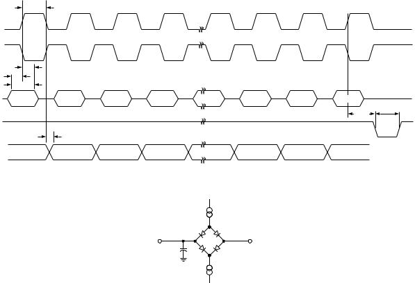
STB1, |
tSTB |
|
|
|
|
|
|
||
STB2, |
|
|
|
|
STB4 |
|
|
|
|
STB3 |
|
|
|
|
|
tDH |
|
|
|
|
tDS |
|
|
|
|
tSRI |
|
|
|
SRI |
DB11(N) |
DB10(N) |
DB0(N) |
|
(MSB) |
||||
|
|
tLD, tCLR |
||
|
|
|
||
|
|
|
tASB |
|
LD1, |
|
|
|
|
LD2, |
|
|
|
|
CLR |
|
tSV |
|
|
SRO |
|
DB10(N–1) |
DB0(N–1) |
Figure 1. AD7943 Timing Diagram
|
1.6mA |
IOL |
TO OUTPUT |
|
+2.1V |
PIN |
CL |
|
|
|
|
|
50pF |
|
|
200mA |
IOH |
Figure 2. Load Circuit for Digital Output Timing Specifications
REV. B |
–5– |
 Loading...