ANALOG DEVICES AD8317 Service Manual

FEATURES
Wide bandwidth: 1 MHz to 10 GHz
High accuracy: ±1.0 dB over temperature
55 dB dynamic range up to 8 GHz ± 3 dB error Stability over temperature: ±0.5 dB
Low noise measurement/controller output, VOUT Pulse response time: 6 ns/10 ns (fall/rise)
Small footprint, 2 mm × 3 mm LFCSP Supply operation: 3.0 V to 5.5 V @ 22 mA Fabricated using high speed SiGe process
APPLICATIONS
RF transmitter PA setpoint control and level monitoring Power monitoring in radio link transmitters
RSSI measurement in base stations, WLANs, WiMAX, and radars
GENERAL DESCRIPTION
The AD8317 is a demodulating logarithmic amplifier, capable of accurately converting an RF input signal to a corresponding decibel-scaled output. It employs the progressive compression technique over a cascaded amplifier chain, each stage of which is equipped with a detector cell. The device can be used in either measurement or controller modes. The AD8317 maintains accurate log conformance for signals of 1 MHz to 8 GHz and provides useful operation to 10 GHz. The input dynamic range is typically 55 dB (re: 50 Ω) with less than ±3 dB error. The AD8317 has 6 ns/10 ns response time (fall time/rise time) that enables RF burst detection to a pulse rate of beyond 50 MHz. The device provides unprecedented logarithmic intercept stability vs. ambient temperature conditions. A supply of 3.0 V to 5.5 V is required to power the device. Current consumption is typically 22 mA, and it decreases to 200 μA when the device is disabled.
The AD8317 can be configured to provide a control voltage to a power amplifier or a measurement output from the VOUT pin. Because the output can be used for controller applications, special attention has been paid to minimize wideband noise. In this mode, the setpoint control voltage is applied to the VSET pin.
Rev. B
Information furnished by Analog Devices is believed to be accurate and reliable. However, no responsibilityisassumedbyAnalogDevicesforitsuse,norforanyinfringementsofpatentsorother rightsofthirdpartiesthatmayresultfromitsuse.Specificationssubjecttochangewithoutnotice.No license is granted by implication or otherwise under any patent or patent rights of Analog Devices. Trademarksandregisteredtrademarksarethepropertyoftheirrespectiveowners.
1 MHz to 10 GHz, 55 dB Log Detector/Controller AD8317
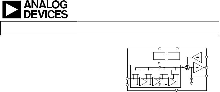
FUNCTIONAL BLOCK DIAGRAM
|
|
VPOS |
TADJ |
|
|
|
|
|
GAIN |
SLOPE |
|
|
|
|
|
BIAS |
I |
V |
VSET |
|
|
|
|
||||
|
|
|
|
I |
V |
VOUT |
DET |
DET |
DET |
DET |
|
|
|
INHI |
|
|
|
|
|
CLPF |
|
|
|
|
|
|
|
INLO |
|
|
|
|
|
|
|
|
|
COMM |
|
|
05541-001 |
Figure 1.
The feedback loop through an RF amplifier is closed via VOUT, the output of which regulates the output of the amplifier to a magnitude corresponding to VSET. The AD8317 provides 0 V to (VPOS − 0.1 V) output capability at the VOUT pin, suitable for controller applications. As a measurement device, VOUT is externally connected to VSET to produce an output voltage, VOUT, that is a decreasing linear-in-dB function of the RF input signal amplitude.
The logarithmic slope is −22 mV/dB, determined by the VSET interface. The intercept is 15 dBm (re: 50 Ω, CW input) using the INHI input. These parameters are very stable against supply and temperature variations.
The AD8317 is fabricated on a SiGe bipolar IC process and is available in a 2 mm × 3 mm, 8-lead LFCSP with an operating temperature range of −40°C to +85°C.
One Technology Way, P.O. Box 9106, Norwood, MA 02062-9106, U.S.A. Tel: 781.329.4700 www.analog.com Fax: 781.461.3113 ©2005–2008 Analog Devices, Inc. All rights reserved.

AD8317
TABLE OF CONTENTS |
|
Features .............................................................................................. |
1 |
Applications....................................................................................... |
1 |
Functional Block Diagram .............................................................. |
1 |
General Description ......................................................................... |
1 |
Revision History ............................................................................... |
2 |
Specifications..................................................................................... |
3 |
Absolute Maximum Ratings............................................................ |
5 |
ESD Caution.................................................................................. |
5 |
Pin Configuration and Function Descriptions............................. |
6 |
Typical Performance Characteristics ............................................. |
7 |
Theory of Operation ...................................................................... |
10 |
Using the AD8317 .......................................................................... |
11 |
Basic Connections ...................................................................... |
11 |
REVISION HISTORY |
|
3/08—Rev. A to Rev. B |
|
Changes to Features.......................................................................... |
1 |
Changes to General Description .................................................... |
1 |
Changes to Measurement Mode Section..................................... |
12 |
Changes to Equation 12 ................................................................. |
15 |
8/07—Rev. 0 to Rev. A |
|
Changes to f = 8.0 GHz, ±1 dB Dynamic Range Parameter ....... |
4 |
Changes to Table 2............................................................................ |
6 |
Changes to Figure 20...................................................................... |
10 |
Changes to Setpoint Interface Section and Figure 22................ |
12 |
Changes Figure 27 .......................................................................... |
13 |
Changes to Table 5.......................................................................... |
17 |
Added Die Information Section ................................................... |
19 |
Changes to Ordering Guide .......................................................... |
21 |
10/05—Revision 0: Initial Version |
|
Input Signal Coupling................................................................ |
11 |
Output Interface ......................................................................... |
11 |
Setpoint Interface ....................................................................... |
11 |
Temperature Compensation of Output Voltage..................... |
12 |
Measurement Mode ................................................................... |
12 |
Setting the Output Slope in Measurement Mode .................. |
13 |
Controller Mode......................................................................... |
13 |
Output Filtering.......................................................................... |
15 |
Operation Beyond 8 GHz ......................................................... |
15 |
Evaluation Board ............................................................................ |
16 |
Die Information.............................................................................. |
18 |
Outline Dimensions ....................................................................... |
19 |
Ordering Guide .......................................................................... |
19 |
Rev. B | Page 2 of 20

AD8317
SPECIFICATIONS
VPOS = 3 V, CLPF = 1000 pF, TA = 25°C, 52.3 Ω termination resistor at INHI, unless otherwise noted.
Table 1.
Parameter |
Conditions |
Min |
Typ |
Max |
Unit |
|
|
|
|
|
|
SIGNAL INPUT INTERFACE |
INHI (Pin 1) |
|
|
|
|
Specified Frequency Range |
|
0.001 |
|
10 |
GHz |
DC Common-Mode Voltage |
|
|
VPOS − 0.6 |
|
V |
MEASUREMENT MODE |
VOUT (Pin 5) shorted to VSET (Pin 4), sinusoidal |
|
|
|
|
|
input signal |
|
|
|
|
f = 900 MHz |
RTADJ = 18 kΩ |
|
|
|
|
Input Impedance |
|
|
1500||0.33 |
|
Ω||pF |
±1 dB Dynamic Range |
TA = 25°C |
|
50 |
|
dB |
|
−40°C < TA < +85°C |
|
46 |
|
dB |
Maximum Input Level |
±1 dB error |
|
−3 |
|
dBm |
Minimum Input Level |
±1 dB error |
|
−53 |
|
dBm |
Slope1 |
|
−25 |
−22 |
−19.5 |
mV/dB |
Intercept1 |
|
12 |
15 |
21 |
dBm |
Output Voltage, High Power In |
PIN = −10 dBm |
0.42 |
0.58 |
0.78 |
V |
Output Voltage, Low Power In |
PIN = −40 dBm |
1.00 |
1.27 |
1.40 |
V |
f = 1.9 GHz |
RTADJ = 8 kΩ |
|
|
|
|
Input Impedance |
|
|
950||0.38 |
|
Ω||pF |
±1 dB Dynamic Range |
TA = 25°C |
|
50 |
|
dB |
|
−40°C < TA < +85°C |
|
48 |
|
dB |
Maximum Input Level |
±1 dB error |
|
−4.00 |
|
dBm |
Minimum Input Level |
±1 dB error |
|
−54 |
|
dBm |
Slope1 |
|
−25 |
−22 |
−19.5 |
mV/dB |
Intercept1 |
|
10 |
14 |
20 |
dBm |
Output Voltage, High Power In |
PIN = −10 dBm |
0.35 |
0.54 |
0.80 |
V |
Output Voltage, Low Power In |
PIN = −35 dBm |
0.75 |
1.21 |
1.35 |
V |
f = 2.2 GHz |
RTADJ = 8 kΩ |
|
|
|
|
Input Impedance |
|
|
810||0.39 |
|
Ω||pF |
±1 dB Dynamic Range |
TA = 25°C |
|
50 |
|
dB |
|
−40°C < TA < +85°C |
|
47 |
|
dB |
Maximum Input Level |
±1 dB error |
|
−5 |
|
dBm |
Minimum Input Level |
±1 dB error |
|
−55 |
|
dBm |
Slope1 |
|
|
−22 |
|
mV/dB |
Intercept1 |
|
|
14 |
|
dBm |
Output Voltage, High Power In |
PIN = −10 dBm |
|
0.53 |
|
V |
Output Voltage, Low Power In |
PIN = −40 dBm |
|
1.20 |
|
V |
f = 3.6 GHz |
RTADJ = 8 kΩ |
|
|
|
|
Input Impedance |
|
|
300||0.33 |
|
Ω||pF |
±1 dB Dynamic Range |
TA = 25°C |
|
42 |
|
dB |
|
−40°C < TA < +85°C |
|
40 |
|
dB |
Maximum Input Level |
±1 dB error |
|
−6 |
|
dBm |
Minimum Input Level |
±1 dB error |
|
−48 |
|
dBm |
Slope1 |
|
|
−22 |
|
mV/dB |
Intercept1 |
|
|
11 |
|
dBm |
Output Voltage, High Power In |
PIN = −10 dBm |
|
0.47 |
|
V |
Output Voltage, Low Power In |
PIN = −40 dBm |
|
1.16 |
|
V |
|
|
|
|
|
|
Rev. B | Page 3 of 20

AD8317
Parameter |
Conditions |
Min |
Typ |
Max |
Unit |
f = 5.8 GHz |
RTADJ = 500 Ω |
|
|
|
|
Input Impedance |
|
|
110||0.05 |
|
Ω||pF |
±1 dB Dynamic Range |
TA = 25°C |
|
50 |
|
dB |
|
−40°C < TA < +85°C |
|
48 |
|
dB |
Maximum Input Level |
±1 dB error |
|
−4 |
|
dBm |
Minimum Input Level |
±1 dB error |
|
−54 |
|
dBm |
Slope1 |
|
|
−22 |
|
mV/dB |
Intercept1 |
|
|
16 |
|
dBm |
Output Voltage, High Power In |
PIN = −10 dBm |
|
0.59 |
|
V |
Output Voltage, Low Power In |
PIN = −40 dBm |
|
1.27 |
|
V |
f = 8.0 GHz |
RTADJ = open |
|
|
|
|
Input Impedance |
|
|
28||0.79 |
|
Ω||pF |
±1 dB Dynamic Range |
TA = 25°C |
|
44 |
|
dB |
|
−40°C < TA < +85°C |
|
35 |
|
dB |
Maximum Input Level |
±1 dB error |
|
−2 |
|
dBm |
Minimum Input Level |
±1 dB error |
|
−46 |
|
dBm |
Slope2 |
|
|
−22 |
|
mV/dB |
Intercept2 |
|
|
21 |
|
dBm |
Output Voltage, High Power In |
PIN = −10 dBm |
|
0.70 |
|
V |
Output Voltage, Low Power In |
PIN = −40 dBm |
|
1.39 |
|
V |
|
|
|
|
|
|
OUTPUT INTERFACE |
VOUT (Pin 5) |
|
|
|
|
Voltage Swing |
VSET = 0 V, RFIN = open |
|
VPOS − 0.1 |
|
V |
|
VSET = 1.7 V, RFIN = open |
|
10 |
|
mV |
Output Current Drive |
VSET = 0 V, RFIN = open |
|
10 |
|
mA |
Small Signal Bandwidth |
RFIN = −10 dBm, from CLPF to VOUT |
|
140 |
|
MHz |
Output Noise |
RFIN = 2.2 GHz, −10 dBm, fNOISE = 100 kHz, |
|
90 |
|
nV/√Hz |
|
CLPF = open |
|
|
|
|
Fall Time |
Input level = no signal to −10 dBm, 90% to 10%, |
|
18 |
|
ns |
|
CLPF = 8 pF |
|
|
|
|
|
Input level = no signal to −10 dBm, 90% to 10%, |
|
6 |
|
ns |
|
CLPF = open, ROUT = 150 Ω |
|
|
|
|
Rise Time |
Input level = −10 dBm to no signal, 10% to 90%, |
|
20 |
|
ns |
|
CLPF = 8 pF |
|
|
|
|
|
Input level = −10 dBm to no signal, 10% to 90%, |
|
10 |
|
ns |
|
CLPF = open, ROUT = 150 Ω |
|
|
|
|
Video Bandwidth (or Envelope Bandwidth) |
|
|
50 |
|
MHz |
|
|
|
|
|
|
VSET INTERFACE |
VSET (Pin 4) |
|
|
|
|
Nominal Input Range |
RFIN = 0 dBm, measurement mode |
|
0.35 |
|
V |
|
RFIN = −50 dBm, measurement mode |
|
1.40 |
|
V |
Logarithmic Scale Factor |
|
|
−45 |
|
dB/V |
Input Resistance |
RFIN = −20 dBm, controller mode, VSET = 1 V |
|
40 |
|
kΩ |
|
|
|
|
|
|
TADJ INTERFACE |
TADJ (Pin 6) |
|
|
|
|
Input Resistance |
TADJ = 0.9 V, sourcing 50 μA |
|
13 |
|
kΩ |
Disable Threshold Voltage |
TADJ = open |
|
VPOS − 0.4 |
|
V |
|
|
|
|
|
|
POWER INTERFACE |
VPOS (Pin 7) |
|
|
|
|
Supply Voltage |
|
3.0 |
|
5.5 |
V |
Quiescent Current |
|
18 |
22 |
30 |
mA |
vs. Temperature |
−40°C ≤ TA ≤ +85°C |
|
60 |
|
μA/°C |
Disable Current |
TADJ = VPOS |
|
200 |
|
μA |
|
|
|
|
|
|
1 Slope and intercept are determined by calculating the best-fit line between the power levels of −40 dBm and −10 dBm at the specified input frequency. 2 Slope and intercept are determined by calculating the best-fit line between the power levels of −34 dBm and −16 dBm at 8.0 GHz.
Rev. B | Page 4 of 20

ABSOLUTE MAXIMUM RATINGS
Table 2.
Parameter |
Rating |
Supply Voltage, VPOS |
5.7 V |
VSET Voltage |
0 V to VPOS |
Input Power (Single-Ended, Re: 50 Ω) |
12 dBm |
Internal Power Dissipation |
0.73 W |
θJA |
55°C/W |
Maximum Junction Temperature |
125°C |
Operating Temperature Range |
−40°C to +85°C |
Storage Temperature Range |
−65°C to +150°C |
Lead Temperature (Soldering, 60 sec) |
260°C |
|
|
AD8317
Stresses above those listed under Absolute Maximum Ratings may cause permanent damage to the device. This is a stress rating only; functional operation of the device at these or any other conditions above those indicated in the operational section of this specification is not implied. Exposure to absolute maximum rating conditions for extended periods may affect device reliability.
ESD CAUTION
Rev. B | Page 5 of 20

AD8317
PIN CONFIGURATION AND FUNCTION DESCRIPTIONS
INHI 1 |
|
|
|
8 |
INLO |
|
AD8317 |
|
|||
|
|
||||
COMM 2 |
|
|
7 VPOS |
||
|
|
||||
|
|
||||
CLPF 3 |
|
TOP VIEW |
|
6 |
TADJ |
|
|
||||
|
(Not to Scale) |
|
|||
VSET 4 |
|
|
5 |
VOUT |
|
|
|
|
|||
|
|
|
|||
|
|
|
|
|
|
|
|
|
|
|
|
Figure 2. Pin Configuration
05541-002
Table 3. Pin Function Descriptions
Pin No. Mnemonic
1INHI
2COMM
3CLPF
4VSET
5VOUT
6TADJ
7VPOS
8INLO Paddle
Description
RF Input. Nominal input range of −50 dBm to 0 dBm, re: 50 Ω; ac-coupled RF input. Device Common. Connect to a low impedance ground plane.
Loop Filter Capacitor. In measurement mode, this capacitor sets the pulse response time and video bandwidth. In controller mode, the capacitance on this node sets the response time of the error amplifier/integrator.
Setpoint Control Input for Controller Mode or Feedback Input for Measurement Mode.
Measurement and Controller Output. In measurement mode, VOUT provides a decreasing linear-in-dB representation of the RF input signal amplitude. In controller mode, VOUT is used to control the gain of a VGA or VVA with a positive gain sense (increasing voltage increases gain).
Temperature Compensation Adjustment. Frequency-dependent temperature compensation is set by connecting a ground-referenced resistor to this pin.
Positive Supply Voltage: 3.0 V to 5.5 V.
RF Common for INHI. AC-coupled RF common.
Internally connected to COMM; solder to a low impedance ground plane.
Rev. B | Page 6 of 20
 Loading...