


 Loading...
Analog Devices AD7854CB, AD7854ARS, AD7854AR, AD7854AQ, AD7854SQ Datasheet
...a |
3 V to 5 V Single Supply, 200 kSPS |
|
12-Bit Sampling ADCs |
||
|
|
|
|
|
AD7854/AD7854L* |
FEATURES
Specified for VDD of 3 V to 5.5 V Read-Only Operation
AD7854–200 kSPS; AD7854L–100 kSPS System and Self-Calibration
Low Power
Normal Operation
AD7854: 15 mW (VDD = 3 V)
AD7854L: 5.5 mW (VDD = 3 V)
Automatic Power-Down After Conversion (25 W)
AD7854: 1.3 mW 10 kSPS AD7854L: 650 W 10 kSPS
Flexible Parallel Interface
12-Bit Parallel/8-Bit Parallel (AD7854)
28-Lead DIP, SOIC and SSOP Packages (AD7854)
APPLICATIONS
Battery-Powered Systems (Personal Digital Assistants,
Medical Instruments, Mobile Communications)
Pen Computers
Instrumentation and Control Systems
High Speed Modems
FUNCTIONAL BLOCK DIAGRAM
|
AVDD |
AGND |
|
AIN(+) |
T/H |
AD7854/AD7854L |
|
|
|
|
|
AIN(–) |
|
|
|
|
2.5V |
|
DVDD |
|
REFERENCE |
|
|
REFIN/ |
|
COMP |
|
BUF |
|
|
|
REFOUT |
|
|
|
|
|
|
|
|
|
|
DGND |
CREF1 |
CHARGE |
|
|
|
REDISTRIBUTION |
|
|
|
DAC |
|
|
|
|
|
CLKIN |
CREF2 |
|
SAR + ADC |
CONVST |
CALIBRATION |
CONTROL |
||
|
|
BUSY |
|
|
MEMORY |
|
|
|
|
|
|
|
AND CONTROLLER |
|
|
|
PARALLEL INTERFACE/CONTROL REGISTER |
|
|
DB11–DB0 CS RD WR HBEN
GENERAL DESCRIPTION
The AD7854/AD7854L is a high speed, low power, 12-bit ADC that operates from a single 3 V or 5 V power supply, the AD7854 being optimized for speed and the AD7854L for low power. The ADC powers up with a set of default conditions at which time it can be operated as a read-only ADC. The ADC contains self-calibration and system calibration options to ensure accurate operation over time and temperature and has a number of power-down options for low power applications.
The AD7854 is capable of 200 kHz throughput rate while the AD7854L is capable of 100 kHz throughput rate. The input track-and-hold acquires a signal in 500 ns and features a pseudodifferential sampling scheme. The AD7854 and AD7854L input
voltage range is 0 to VREF (unipolar) and –VREF/2 to +VREF/2, centered at VREF/2 (bipolar). The coding is straight binary in
unipolar mode and twos complement in bipolar mode. Input signal range is to the supply and the part is capable of converting full-power signals to 100 kHz.
CMOS construction ensures low power dissipation of typically 5.4 mW for normal operation and 3.6 W in power-down mode. The part is available in 28-lead, 0.6 inch wide dual-in-line package (DIP), 28-lead small outline (SOIC) and 28-lead small shrink outline (SSOP) packages.
*Patent pending.
See Page 27 for data sheet index.
PRODUCT HIGHLIGHTS
1.Operation with either 3 V or 5 V power supplies.
2.Flexible power management options including automatic power-down after conversion. By using the power management options a superior power performance at slower throughput rates can be achieved:
AD7854: 1 mW typ @ 10 kSPS AD7854L: 1 mW typ @ 20 kSPS
3.Operates with reference voltages from 1.2 V to AVDD.
4.Analog input ranges from 0 V to AVDD.
5.Self-calibration and system calibration.
6.Versatile parallel I/O port.
7.Lower power version AD7854L.
REV. B
Information furnished by Analog Devices is believed to be accurate and reliable. However, no responsibility is assumed by Analog Devices for its use, nor for any infringements of patents or other rights of third parties which may result from its use. No license is granted by implication or otherwise under any patent or patent rights of Analog Devices.
One Technology Way, P.O. Box 9106, Norwood, MA 02062-9106, U.S.A.
Tel: 781/329-4700 |
World Wide Web Site: http://www.analog.com |
Fax: 781/326-8703 |
© Analog Devices, Inc., 2000 |

AD7854/AD7854L–SPECIFICATIONS1, 2 (AVDD = DVDD = +3.0 V to +5.5 V, REFIN/REFOUT = 2.5 V External Reference, fCLKIN = 4 MHz (for L Version: 1.8 MHz (0 C to +70 C) and 1 MHz (–40 C to +85 C)); fSAMPLE = 200 kHz (AD7854), 100 kHz
(AD7854L); TA = TMIN to TMAX, unless otherwise noted.) Specifications in () apply to the AD7854L.
Parameter |
A Version1 |
B Version1 |
S Version1 |
Units |
Test Conditions/Comments |
DYNAMIC PERFORMANCE |
|
|
|
|
|
Signal to Noise + Distortion Ratio3 |
70 |
71 |
70 |
dB min |
Typically SNR is 72 dB |
(SNR) |
|
|
|
|
VIN = 10 kHz Sine Wave, fSAMPLE = 200 kHz |
|
|
|
|
|
(L Version: fSAMPLE = 100 kHz @ fCLKIN = 2 MHz) |
Total Harmonic Distortion (THD) |
–78 |
–78 |
–78 |
dB max |
VIN = 10 kHz Sine Wave, fSAMPLE = 200 kHz |
|
|
|
|
|
(L Version: fSAMPLE = 100 kHz @ fCLKIN = 2 MHz) |
Peak Harmonic or Spurious Noise |
–78 |
–78 |
–78 |
dB max |
VIN = 10 kHz Sine Wave, fSAMPLE = 200 kHz |
|
|
|
|
|
(L Version: fSAMPLE = 100 kHz @ fCLKIN = 2 MHz) |
Intermodulation Distortion (IMD) |
|
|
|
|
|
Second Order Terms |
–78 |
–78 |
–78 |
dB typ |
fa = 9.983 kHz, fb = 10.05 kHz, fSAMPLE = 200 kHz |
|
|
|
|
|
(L Version: fSAMPLE = 100 kHz @ fCLKIN = 2 MHz) |
Third Order Terms |
–78 |
–78 |
–78 |
dB typ |
fa = 9.983 kHz, fb = 10.05 kHz, fSAMPLE = 200 kHz |
|
|
|
|
|
(L Version: fSAMPLE = 100 kHz @ fCLKIN = 2 MHz) |
DC ACCURACY |
|
|
|
|
|
Resolution |
12 |
12 |
12 |
Bits |
|
Integral Nonlinearity |
±1 |
±0.5 |
±1 |
LSB max |
5 V Reference VDD = 5 V |
Differential Nonlinearity |
±1 |
±1 |
±1 |
LSB max |
Guaranteed No Missed Codes to 12 Bits |
Unipolar Offset Error |
±3 |
±3 |
±4 |
LSB max |
|
|
±2 |
±2 |
±2 |
LSB typ |
|
Unipolar Gain Error |
±4 |
±4 |
±4 |
LSB max |
|
|
±2 |
±2 |
±2 |
LSB typ |
|
Bipolar Positive Full-Scale Error |
±4 |
±4 |
±5 |
LSB max |
|
|
±2 |
±2 |
±2 |
LSB typ |
|
Negative Full-Scale Error |
±4 |
±4 |
±5 |
LSB max |
|
|
±2 |
±2 |
±2 |
LSB typ |
|
Bipolar Zero Error |
±4 |
±4 |
±5 |
LSB max |
|
|
|
|
|
|
|
ANALOG INPUT |
|
|
|
|
|
Input Voltage Ranges |
0 to VREF |
0 to VREF |
0 to VREF |
Volts |
i.e., AIN(+) – AIN(–) = 0 to VREF, AIN(–) can be |
|
±VREF/2 |
±VREF/2 |
±VREF/2 |
|
biased up but AIN(+) cannot go below AIN(–). |
|
Volts |
i.e., AIN(+) – AIN(–) = –VREF/2 to +VREF/2, AIN(–) |
|||
|
|
|
|
|
should be biased to +VREF/2 and AIN(+) can go below |
|
±1 |
±1 |
±1 |
µA max |
AIN(–) but cannot go below 0 V. |
Leakage Current |
|
||||
Input Capacitance |
20 |
20 |
20 |
pF typ |
|
|
|
|
|
|
|
REFERENCE INPUT/OUTPUT |
|
|
|
|
|
REFIN Input Voltage Range |
2.3/VDD |
2.3/VDD |
2.3/VDD |
V min/max |
Functional from 1.2 V |
Input Impedance |
150 |
150 |
150 |
kΩ typ |
|
REFOUT Output Voltage |
2.3/2.75 |
2.3/2.7 |
2.3/2.7 |
V min/max |
|
REFOUT Tempco |
20 |
20 |
20 |
ppm/°C typ |
|
LOGIC INPUTS |
|
|
|
|
|
Input High Voltage, VINH |
3 |
3 |
3 |
V min |
AVDD = DVDD = 4.5 V to 5.5 V |
|
2.1 |
2.1 |
2.1 |
V min |
AVDD = DVDD = 3.0 V to 3.6 V |
Input Low Voltage, VINL |
0.4 |
0.4 |
0.4 |
V max |
AVDD = DVDD = 4.5 V to 5.5 V |
|
0.6 |
0.6 |
0.6 |
V max |
AVDD = DVDD = 3.0 V to 3.6 V |
Input Current, IIN |
±10 |
±10 |
±10 |
µA max |
Typically 10 nA, VIN = 0 V or VDD |
Input Capacitance, CIN4 |
10 |
10 |
10 |
pF max |
|
LOGIC OUTPUTS |
|
|
|
|
ISOURCE = 200 µA |
Output High Voltage, VOH |
|
|
|
|
|
|
4 |
4 |
4 |
V min |
AVDD = DVDD = 4.5 V to 5.5 V |
|
2.4 |
2.4 |
2.4 |
V min |
AVDD = DVDD = 3.0 V to 3.6 V |
Output Low Voltage, VOL |
0.4 |
0.4 |
0.4 |
V max |
ISINK = 0.8 mA |
Floating-State Leakage Current |
±10 |
±10 |
±10 |
µA max |
|
Floating-State Output Capacitance4 |
10 |
10 |
10 |
pF max |
|
Output Coding |
Straight (Natural) |
Binary |
|
Unipolar Input Range |
|
|
|
Twos Complement |
|
Bipolar Input Range |
|
|
|
|
|
|
|
CONVERSION RATE |
|
|
|
|
tCLKIN × 18 |
Conversion Time |
4.6 (10) |
4.6 (9) |
4.6 (9) |
µs max |
(L Versions Only, 0°C to +70°C, 1.8 MHz CLKIN) |
Track/Hold Acquisition Time |
0.5 (1) |
0.5 (1) |
0.5 (1) |
µs min |
(L Versions Only, –40°C to +85°C, 1 MHz CLKIN) |
|
|
|
|
|
|
–2– |
REV. B |

|
|
|
|
|
|
|
AD7854/AD7854L |
|
|
|
|
|
|
|
|
||
Parameter |
A Version1 |
B Version1 |
S Version1 |
Units |
Test Conditions/Comments |
|||
POWER REQUIREMENTS |
|
|
|
|
|
|
|
|
AVDD, DVDD |
+3.0/+5.5 |
+3.0/+5.5 |
+3.0/+5.5 |
V min/max |
|
|
||
IDD |
|
|
|
|
|
|
|
|
Normal Mode5 |
5.5 (1.8) |
5.5 (1.8) |
6 (1.8) |
mA max |
AVDD = DVDD = 4.5 V to 5.5 V. Typically 4.5 mA |
|||
|
|
|
|
|
|
|
(1.5 mA); |
|
|
5.5 (1.8) |
5.5 (1.8) |
6 (1.8) |
mA max |
AVDD = DVDD = 3.0 V to 3.6 V. Typically 4.0 mA |
|||
Sleep Mode6 |
|
|
|
|
|
|
(1.5 mA). |
|
|
|
|
|
|
µA typ |
|
|
|
With External Clock On |
10 |
10 |
|
10 |
|
Full power-down. Power management bits in control |
||
|
|
|
|
|
|
µA typ |
register set as PMGT1 = 1, PMGT0 = 0. |
|
|
400 |
400 |
400 |
Partial power-down. Power management bits in |
||||
|
|
|
|
|
|
|
control register set as PMGT1 = 1, PMGT0 = 1. |
|
With External Clock Off |
5 |
5 |
|
5 |
|
µA max |
Typically 1 µA. Full power-down. Power management |
|
|
|
|
|
|
|
|
bits in control register set as PMGT1 = 1, |
|
|
|
|
|
|
|
µA typ |
PMGT0 = 0. |
|
|
200 |
200 |
200 |
Partial power-down. Power management bits in |
||||
|
|
|
|
|
|
|
control register set as PMGT1 = 1, PMGT0 = 1. |
|
Normal Mode Power Dissipation |
30 (10) |
30 |
(10) |
30 |
(10) |
mW max |
VDD = 5.5 V: Typically 25 mW (8) |
|
|
20 (6.5) |
20 |
(6.5) |
20 |
(6.5) |
mW max |
VDD = 3.6 V: Typically 15 mW (5.4) |
|
Sleep Mode Power Dissipation |
|
|
|
|
|
µW typ |
|
|
With External Clock On |
55 |
55 |
|
55 |
|
VDD = 5.5 V |
||
|
36 |
36 |
|
36 |
|
µW typ |
VDD = 3.6 V |
|
With External Clock Off |
27.5 |
27.5 |
27.5 |
µW max |
VDD = 5.5 V: Typically 5.5 µW |
|||
|
18 |
18 |
|
18 |
|
µW max |
VDD = 3.6 V: Typically 3.6 µW |
|
SYSTEM CALIBRATION |
+0.05 × VREF/–0.05 × VREF |
|
|
|
||||
Offset Calibration Span7 |
V max/min |
Allowable Offset Voltage Span for Calibration |
||||||
Gain Calibration Span7 |
+0.025 × VREF/–0.025 × VREF |
V max/min |
Allowable Full-Scale Voltage Span for Calibration |
|
||||
NOTES
1Temperature ranges as follows: A, B Versions, –40°C to +85°C; S Version, –55°C to +125°C. 2Specifications apply after calibration.
3Not production tested. Guaranteed by characterization at initial product release.
4Sample tested @ +25°C to ensure compliance.
5All digital inputs @ DGND except for CONVST @ DVDD. No load on the digital outputs. Analog inputs @ AGND.
6CLKIN @ DGND when external clock off. All digital inputs @ DGND except for CONVST @ DVDD. No load on the digital outputs. Analog inputs @ AGND. 7The offset and gain calibration spans are defined as the range of offset and gain errors that the AD7854/AD7854L can calibrate. Note also that these are voltage spans and are not absolute voltages (i.e., the allowable system offset voltage presented at AIN(+) for the system offset error to be adjusted out will be AIN(–) ± 0.05 × VREF, and the allowable system full-scale voltage applied between AIN(+) and AIN(–) for the system full-scale voltage error to be adjusted out will be VREF ± 0.025 × VREF (unipolar mode) and VREF/2 ± 0.025 × VREF (bipolar mode)). This is explained in more detail in the calibration section of the data sheet.
Specifications subject to change without notice.
REV. B |
–3– |
AD7854/AD7854L
|
|
|
(AVDD = DVDD = +3.0 V to +5.5 V; fCLKIN = 4 MHz for AD7854 and 1.8 MHz for AD7854L; |
||
TIMING SPECIFICATIONS1 TA = TMIN to TMAX, unless otherwise noted) |
|||||
|
Limit at TMIN, TMAX |
|
|
||
|
(A, B, S Versions) |
|
|
||
Parameter |
5 V |
|
3 V |
Units |
Description |
|
|||||
|
|
|
|
|
|
2 |
500 |
|
500 |
kHz min |
Master Clock Frequency |
fCLKIN |
|
||||
|
4 |
|
4 |
MHz max |
|
t13 |
1.8 |
|
1.8 |
MHz max |
L Version |
100 |
|
100 |
ns min |
CONVST Pulsewidth |
|
t2 |
50 |
|
90 |
ns max |
CONVST to BUSY ↑ Propagation Delay |
tCONVERT |
4.5 |
|
4.5 |
µs max |
Conversion Time = 18 tCLKIN |
|
10 |
|
10 |
µs max |
L Version 1.8 MHz CLKIN. Conversion Time = 18 tCLKIN |
t3 |
15 |
|
15 |
ns min |
HBEN to RD Setup Time |
t4 |
5 |
|
5 |
ns min |
HBEN to RD Hold Time |
t5 |
0 |
|
0 |
ns min |
CS to RD to Setup Time |
t6 |
0 |
|
0 |
ns min |
CS to RD Hold Time |
t7 |
55 |
|
70 |
ns min |
RD Pulsewidth |
t84 |
50 |
|
50 |
ns max |
Data Access Time After RD |
t95 |
5 |
|
5 |
ns min |
Bus Relinquish Time After RD |
|
40 |
|
40 |
ns max |
|
t10 |
60 |
|
70 |
ns min |
Minimum Time Between Reads |
t11 |
0 |
|
0 |
ns min |
HBEN to WR Setup Time |
t12 |
5 |
|
5 |
ns max |
HBEN to WR Hold Time |
t13 |
0 |
|
0 |
ns min |
CS to WR Setup Time |
t14 |
0 |
|
0 |
ns max |
CS to WR Hold Time |
t15 |
55 |
|
70 |
ns min |
WR Pulsewidth |
t16 |
10 |
|
10 |
ns min |
Data Setup Time Before WR |
t17 |
5 |
|
5 |
ns min |
Data Hold Time After WR |
t184 |
1/2 tCLKIN |
|
1/2 tCLKIN |
ns min |
New Data Valid Before Falling Edge of BUSY |
t19 |
50 |
|
70 |
ns min |
HBEN High Pulse Duration |
t20 |
50 |
|
70 |
ns min |
HBEN Low Pulse Duration |
t21 |
40 |
|
60 |
ns min |
Propagation Delay from HBEN Rising Edge to Data Valid |
t22 |
40 |
|
60 |
ns min |
Propagation Delay from HBEN Falling Edge to Data Valid |
t23 |
2.5 tCLKIN |
|
2.5 tCLKIN |
ns max |
CS↑ to BUSY ↑ in Calibration Sequence |
6 |
31.25 |
|
31.25 |
ms typ |
Full Self-Calibration Time, Master Clock Dependent (125013 |
tCAL |
|
||||
6 |
|
|
|
|
tCLKIN) |
27.78 |
|
27.78 |
ms typ |
Internal DAC Plus System Full-Scale Cal Time, Master Clock |
|
tCAL1 |
|
||||
6 |
|
|
|
|
Dependent (111124 tCLKIN) |
3.47 |
|
3.47 |
ms typ |
System Offset Calibration Time, Master Clock Dependent |
|
tCAL2 |
|
||||
|
|
|
|
|
(13889 tCLKIN) |
NOTES
1Sample tested at +25°C to ensure compliance. All input signals are specified with tr = tf = 5 ns (10% to 90% of V DD) and timed from a voltage level of 1.6 V.
2Mark/Space ratio for the master clock input is 40/60 to 60/40.
3The CONVST pulsewidth here only applies for normal operation. When the part is in power-down mode, a different CONVST pulsewidth applies (see Power-Down section).
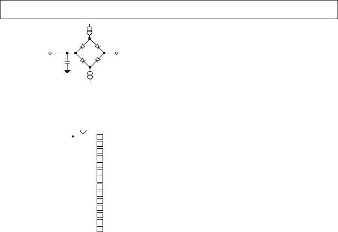
4Measured with the load circuit of Figure 1 and defined as the time required for the output to cross 0.8 V or 2.4 V.
5t9 is derived form the measured time taken by the data outputs to change 0.5 V when loaded with the circuit of Figure 1. The measured number is then extrapolated back to remove the effects of charging or discharging the 50 pF capacitor. This means that the time, t 9, quoted in the timing characteristics is the true bus relinquish time of the part and is independent of the bus loading.
6The typical time specified for the calibration times is for a master clock of 4 MHz. For the L version the calibration times will be longer than those quoted here due to the 1.8 MHz master clock.
Specifications subject to change without notice.
–4– |
REV. B |
AD7854/AD7854L
|
1.6mA |
IOL |
TO |
|
|
OUTPUT |
|
+2.1V |
PIN |
CL |
|
|
50pF |
|
|
200µA |
IOH |
Figure 1. Load Circuit for Digital Output Timing Specifications
PIN CONFIGURATION
FOR DIP, SOIC AND SSOP
|
|
|
|
|
|
|
|
|
|
CONVST |
1 |
|
|
|
28 |
BUSY |
|
|
|
|
|
|
|
|
|
|
|
|
WR |
2 |
|
|
|
27 |
CLKIN |
|
|
|
|
|
|
|
|
|
|
|
RD |
3 |
|
|
|
26 |
DB11 |
|
|
|
|
|
|
|
|
|
|
|
CS |
4 |
|
|
|
25 |
DB10 |
|
|
|
|
|
|
|
|
|
REF |
|
/REF |
5 |
AD7854 |
24 |
DB9 |
||
|
IN |
OUT |
|
|
|
|||
|
|
AVDD |
6 |
TOP VIEW |
23 |
DGND |
||
|
|
|
|
(Not to Scale) |
|
|
||
|
|
AGND |
7 |
22 |
DVDD |
|||
|
|
|
|
|
|
|
|
|
|
|
CREF1 |
8 |
|
|
|
21 |
DB8 |
|
|
|
|
|
|
|
|
|
|
|
CREF2 |
9 |
|
|
|
20 |
DB7 |
|
|
|
|
|
|
19 |
|
|
|
|
AIN(+) |
10 |
|
|
|
DB6 |
|
|
|
|
|
|
|
18 |
|
|
|
|
AIN(–) |
11 |
|
|
|
DB5 |
|
|
|
|
|
|
|
17 |
|
|
|
|
HBEN |
12 |
|
|
|
DB4 |
|
|
|
|
|
|
|
16 |
|
|
|
|
DB0 |
13 |
|
|
|
DB3 |
|
|
|
|
|
|
|
|
|
|
|
|
DB1 |
14 |
|
|
|
15 |
DB2 |
|
|
|
|
|
|
|
|
|
ABSOLUTE MAXIMUM RATINGS1
(TA = +25°C unless otherwise noted)
AVDD to AGND . . . . . . . . . . |
. . . . . . . |
. . . . . |
. –0.3 V to +7 V |
DVDD to DGND . . . . . . . . . . |
. . . . . . . |
. . . . . |
. –0.3 V to +7 V |
AVDD to DVDD . . . . . . . . . . . |
. . . . . . . |
. . . . . |
–0.3 V to +0.3 V |
Analog Input Voltage to AGND . . . . |
–0.3 V to AVDD + 0.3 V |
||
Digital Input Voltage to DGND . . . . |
–0.3 V to DVDD + 0.3 V |
||
Digital Output Voltage to DGND . . . |
–0.3 V to DVDD + 0.3 V |
||
REFIN/REFOUT to AGND . . . |
. . . . . . |
–0.3 V to AVDD + 0.3 V |
|
Input Current to Any Pin Except Supplies2 . . |
. . . . . . . ± 10 mA |
||
Operating Temperature Range |
|
|
–40°C to +85°C |
Commercial (A, B Versions) |
. . . . . . |
. . . . . |
|
Commercial (S Version) . . . |
. . . . . . . |
. . . . |
–55°C to +125°C |
Storage Temperature Range |
. . . . . . . |
. . . . |
–65°C to +150°C |
Junction Temperature . . . . . . |
. . . . . . . |
. . . . . |
. . . . . . . +150°C |
Cerdip Package, Power Dissipation . . . |
. . . . . |
. . . . . . 450 mW |
|
θJA Thermal Impedance . . . |
. . . . . . . |
. . . . . |
. . . . . . . 75°C/W |
Lead Temperature, (Soldering, 10 secs) . . |
. . . . . . . +300°C |
||
SOIC, SSOP Package, Power Dissipation . . . |
. . . . . . 450 mW |
||
θJA Thermal Impedance . . . |
75°C/W (SOIC) 115°C/W (SSOP) |
||
θJC Thermal Impedance . . . |
25°C/W (SOIC) 35°C/W (SSOP) |
||
Lead Temperature, Soldering |
|
+215°C |
|
Vapor Phase (60 secs) . . . |
. . . . . . . |
. . . . . |
|
Infrared (15 secs) . . . . . . |
. . . . . . . |
. . . . . |
. . . . . . . +220°C |
NOTES
1Stresses above those listed under Absolute Maximum Ratings may cause permanent damage to the device. This is a stress rating only; functional operation of the device at these or any other conditions above those listed in the operational sections of this specification is not implied. Exposure to absolute maximum rating conditions for extended periods may affect device reliability.
2Transient currents of up to 100 mA will not cause SCR latchup.
ORDERING GUIDE
|
|
Linearity |
Power |
|
|
Temperature |
Error |
Dissipation |
Package |
Model |
Range1 |
(LSB) |
(mW) |
Option2 |
AD7854AQ |
–40°C to +85°C |
1 |
15 |
Q-28 |
AD7854SQ |
–55°C to +125°C |
1 |
15 |
Q-28 |
AD7854AR |
–40°C to +85°C |
1 |
15 |
R-28 |
AD7854BR |
–40°C to +85°C |
1/2 |
15 |
R-28 |
AD7854ARS |
–40°C to +85°C |
1 |
15 |
RS-28 |
AD7854LAQ3 |
–40°C to +85°C |
1 |
5.5 |
Q-28 |
AD7854LAR3 |
–40°C to +85°C |
1 |
5.5 |
R-28 |
AD7854LARS3 |
–40°C to +85°C |
1 |
5.5 |
RS-28 |
EVAL-AD7854CB4 |
|
|
|
|
EVAL-CONTROL BOARD5 |
|
|
|
|
NOTES
1Linearity error refers to the integral linearity error. 2Q = Cerdip; R = SOIC; RS = SSOP.
3L signifies the low power version.
4This can be used as a stand-alone evaluation board or in conjunction with the EVAL-CONTROL BOARD for evaluation/demonstration purposes.
5This board is a complete unit allowing a PC to control and communicate with all Analog Devices evaluation boards ending in the CB designator. For more information on Analog Devices products and evaluation boards visit our World Wide Web home page at http://www.analog.com.
REV. B |
–5– |

AD7854/AD7854L
PIN FUNCTION DESCRIPTIONS
Pin Mnemonic Description
1CONVST Convert Start. Logic input. A low to high transition on this input puts the track/hold into its hold
|
|
mode and starts conversion. When this input is not used, it should be tied to DVDD. |
2 |
WR |
Write Input. Active low logic input. Used in conjunction with CS and HBEN to write to internal registers. |
3 |
RD |
Read Input. Active low logic input. Used in conjunction with CS and HBEN to read from internal |
|
|
registers. |
4 |
CS |
Chip Select Input. Active low logic input. The device is selected when this input is active. |
5 |
REFIN/ |
Reference Input/Output. This pin is connected to the internal reference through a series resistor and is the |
|
REFOUT |
reference source for the analog-to-digital converter. The nominal reference voltage is 2.5 V and this appears |
|
|
at the pin. This pin can be overdriven by an external reference and can be taken as high as AVDD. When |
|
|
this pin is tied to AVDD, then the CREF1 pin should also be tied to AVDD. |
6 |
AVDD |
Analog Positive Supply Voltage, +3.0 V to +5.5 V. |
7 |
AGND |
Analog Ground. Ground reference for track/hold, reference and DAC. |
8 |
CREF1 |
Reference Capacitor (0.1 µF multilayer ceramic). This external capacitor is used as a charge source for the |
|
|
internal DAC. The capacitor should be tied between the pin and AGND. |
9 |
CREF2 |
Reference Capacitor (0.01 µF ceramic disc). This external capacitor is used in conjunction with the on-chip |
|
|
reference. The capacitor should be tied between the pin and AGND. |
10 |
AIN(+) |
Analog Input. Positive input of the pseudo-differential analog input. Cannot go below AGND or above |
|
|
AVDD at any time, and cannot go below AIN(–) when the unipolar input range is selected. |
11 |
AIN(–) |
Analog Input. Negative input of the pseudo-differential analog input. Cannot go below AGND or above |
|
|
AVDD at any time. |
12 |
HBEN |
High Byte Enable Input. The AD7854 operates in byte mode only but outputs 12 bits of data during a read |
|
|
cycle with HBEN low. When HBEN is high, then the high byte of data that is written to or read from the |
|
|
part is on DB0 to DB7. When HBEN is low, then the lowest byte of data being written to the part is on |
|
|
DB0 to DB7. If reading from the part with HBEN low, then the lowest 12 bits of data appear on pins DB0 |
|
|
to DB11. This allows a single read from the ADC or from the control register in a 16-bit bus system. |
|
|
However, two reads are needed to access the calibration registers. Also, two writes are necessary to write to |
|
|
any of the registers. |
13–21 |
DB0–DB8 |
Data Bits 0 to 8. Three state data I/O pins that are controlled by CS, RD, WR and HBEN. Data output is |
|
|
straight binary (unipolar mode) or twos complement (bipolar mode). |
22 |
DVDD |
Digital Supply Voltage, +3.0 V to +5.5 V. |
23 |
DGND |
Digital Ground. Ground reference point for digital circuitry. |
24–26 |
DB9–DB11 |
Data Bits 9 to 11. Three state data output pins that are controlled by CS, RD and HBEN. Data output is |
|
|
straight binary (unipolar mode) or twos complement (bipolar mode). These output pins should be tied to |
|
|
DVDD via 100 kΩ resistors when the AD7854/AD7854L is being interfaced to an 8-bit data bus. |
27 |
CLKIN |
Master Clock Signal for the device (4 MHz for AD7854, 1.8 MHz for AD7854L). Sets the conversion and |
|
|
calibration times. |
28 |
BUSY |
Busy Output. The busy output is triggered high by the falling edge of CONVST and remains high until |
|
|
conversion is completed. BUSY is also used to indicate when the AD7854/AD7854L has completed its on- |
|
|
chip calibration sequence. |
–6– |
REV. B |

AD7854/AD7854L
TERMINOLOGY Integral Nonlinearity
This is the maximum deviation from a straight line passing through the endpoints of the ADC transfer function. The endpoints of the transfer function are zero scale, a point 1/2 LSB below the first code transition, and full scale, a point 1/2 LSB above the last code transition.
Differential Nonlinearity
This is the difference between the measured and the ideal 1 LSB change between any two adjacent codes in the ADC.
Unipolar Offset Error
This is the deviation of the first code transition (00 . . . 000 to 00 . . . 001) from the ideal AIN(+) voltage (AIN(–) + 1/2 LSB) when operating in the unipolar mode.
Unipolar Gain Error
This is the deviation of the last code transition (111 . . . 110 to
111 . . . 111) from the ideal, i.e., AIN(–) +VREF/2 – 1.5 LSB, after the unipolar offset error has been adjusted out.
Bipolar Positive Full-Scale Error
This applies to the bipolar modes only and is the deviation of the last code transition from the ideal AIN(+) voltage. For bipolar mode, the ideal AIN(+) voltage is (AIN(–) +VREF/2 – 1.5 LSB).
Negative Full-Scale Error
This applies to the bipolar mode only and is the deviation of the first code transition (10 . . . 000 to 10 . . . 001) from the ideal AIN(+) voltage (AIN(–) – VREF/2 + 0.5 LSB).
Bipolar Zero Error
This is the deviation of the midscale transition (all 0s to all 1s) from the ideal AIN(+) voltage (AIN(–) – 1/2 LSB).
Track/Hold Acquisition Time
The track/hold amplifier returns into track mode and the end of conversion. Track/Hold acquisition time is the time required for the output of the track/hold amplifier to reach its final value, within ±1/2 LSB, after the end of conversion.
Signal to (Noise + Distortion) Ratio
This is the measured ratio of signal to (noise + distortion) at the output of the A/D converter. The signal is the rms amplitude of the fundamental. Noise is the sum of all nonfundamental signals up to half the sampling frequency (fS/2), excluding dc. The ratio is dependent on the number of quantization levels in the digitization process; the more levels, the smaller the quantization noise. The theoretical signal to (noise + distortion) ratio for an ideal N-bit converter with a sine wave input is given by:
Signal to (Noise + Distortion) = (6.02 N + 1.76) dB
Thus for a 12-bit converter, this is 74 dB.
Total Harmonic Distortion
Total harmonic distortion (THD) is the ratio of the rms sum of harmonics to the fundamental. For the AD7854/AD7854L, it is defined as:
= (V22 +V32 +V 42 +V52 +V62 )
THD (dB) 20 log
V1
where V1 is the rms amplitude of the fundamental and V2, V3, V4, V5 and V6 are the rms amplitudes of the second through the sixth harmonics.
Peak Harmonic or Spurious Noise
Peak harmonic or spurious noise is defined as the ratio of the rms value of the next largest component in the ADC output spectrum (up to fS/2 and excluding dc) to the rms value of the fundamental. Normally, the value of this specification is determined by the largest harmonic in the spectrum, but for ADCs where the harmonics are buried in the noise floor, it will be a noise peak.
Intermodulation Distortion
With inputs consisting of sine waves at two frequencies, fa and fb, any active device with nonlinearities will create distortion products at sum and difference frequencies of mfa ± nfb where m, n = 0, 1, 2, 3, etc. Intermodulation distortion terms are those for which neither m nor n are equal to zero. For example, the second order terms include (fa + fb) and (fa – fb), while the third order terms include (2fa + fb), (2fa – fb), (fa + 2fb) and (fa – 2fb).
Testing is performed using the CCIF standard where two input frequencies near the top end of the input bandwidth are used. In this case, the second order terms are usually distanced in frequency from the original sine waves while the third order terms are usually at a frequency close to the input frequencies. As a result, the second and third order terms are specified separately. The calculation of the intermodulation distortion is as per the THD specification where it is the ratio of the rms sum of the individual distortion products to the rms amplitude of the sum of the fundamentals expressed in dBs.
REV. B |
–7– |
AD7854/AD7854L
AD7854/AD7854L ON-CHIP REGISTERS
The AD7854/AD7854L powers up with a set of default conditions, and the user need not ever write to the device. In this case the AD7854/AD7854L will operate as a read-only ADC. The WR pin should be tied to DVDD for operating the AD7854/AD7854L as a read-only ADC.
Extra features and flexibility such as performing different power-down options, different types of calibrations including system calibration, and software conversion start can be selected by writing to the part.
The AD7854/AD7854L contains a control register, ADC output data register, status register, test register and 10 calibration registers. The control register is write-only, the ADC output data register and the status register are read-only, and the test and calibration registers are both read/write registers. The test register is used for testing the part and should not be written to.
Addressing the On-Chip Registers
Writing
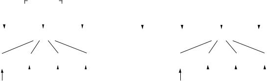
To write to the AD7854/AD7854L, a 16-bit word of data must be transferred. This transfer consists of two 8-bit writes. The first 8 bits of data that are written must consist of the 8 LSBs of the 16-bit word and the second 8 bits that are written must consist of the 8 MSBs of the 16-bit word. For each of these 8-bit writes, the data is placed on Pins DB0 to DB7, Pin DB0 being the LSB of each transfer and Pin DB7 being the MSB of each transfer. The two MSBs of the 16-bit word, ADDR1 and ADDR0, are decoded to determine which register is addressed, and the 14 LSBs are written to the addressed register. Table I shows the decoding of the address bits, while Figure 2 shows the overall write register hierarchy.
|
|
Table I. Write Register Addressing |
|
|
|
ADDR1 |
ADDR0 |
Comment |
|
|
|
0 |
0 |
This combination does not address any register. |
0 |
1 |
This combination addresses the TEST REGISTER. The 14 LSBs of data are written to the test register. |
1 |
0 |
This combination addresses the CALIBRATION REGISTER. The 14 least significant data bits are writ- |
|
|
ten to the selected calibration register. |
1 |
1 |
This combination addresses the CONTROL REGISTER. The 14 least significant data bits are written to |
|
|
the control register. |
|
|
|
Reading
To read from the various registers the user must first write to Bits 6 and 7 in the Control Register, RDSLT0 and RDSLT1. These bits are decoded to determine which register is addressed during a read operation. Table II shows the decoding of the read address bits while Figure 3 shows the overall read register hierarchy. The power-up status of these bits is 00 so that the default read will be from the ADC output data register. Note: when reading from the calibration registers, the low byte must always be read first.
Once the read selection bits are set in the control register all subsequent read operations that follow are from the selected register until the read selection bits are changed in the control register.
|
|
|
|
|
|
|
|
|
|
|
|
|
|
Table II. Read Register Addressing |
||||||||||||||||
|
|
|
|
|
|
|
|
|
|
|
|
|
|
|
|
|
|
|
|
|
|
|
|
|
|
|
|
|
|
|
RDSLT1 |
RDSLT0 |
Comment |
||||||||||||||||||||||||||||
|
|
|
|
|
|
|
|
|
|
|
|
|
|
|
|
|
|
|
|
|
|
|
|
|
|
|
|
|
|
|
0 |
0 |
All successive read operations are from the ADC OUTPUT DATA REGISTER. This is the default power- |
||||||||||||||||||||||||||||
|
|
up setting. There is always four leading zeros when reading from the ADC output data register. |
||||||||||||||||||||||||||||
0 |
1 |
All successive read operations are from the TEST REGISTER. |
||||||||||||||||||||||||||||
1 |
0 |
All successive read operations are from the CALIBRATION REGISTERS. |
||||||||||||||||||||||||||||
1 |
1 |
All successive read operations are from the STATUS REGISTER. |
||||||||||||||||||||||||||||
|
|
|
|
|
|
|
|
|
|
|
|
|
|
|
|
|
|
|
|
|
|
|
|
|
|
|
|
|
|
|
|
|
|
|
|
|
|
|
|
|
|
|
|
|
|
|
|
|
|
|
|
|
|
|
|
|
|
|
|
|
|
|
|
|
|
|
|
|
|
|
|
|
|
|
|
|
|
|
|
|
|
|
|
|
|
|
|
|
|
|
|
|
|
|
|
|
|
|
|
|
|
|
|
|
|
|
|
|
|
|
|
|
|
|
|
|
ADDR1, ADDR0 |
|
|
|
|
|
|
|
|
|
|
|
|
|
|
|
|
|
|
|
|
|
|
|
|
|
|
|
|
|
|
|
RDSLT1, RDSLT0 |
|
|
|
|
|
|
|||||||||||||||||||||||||||||
|
|
|
|
|
|
|
|
|
|
|
|
|
|
|
|
|
|
|
|
|
|
|
|
|
|
|
DECODE |
|
|
|
|
|
|
|
|
|
|
|
|
|
|
|
|
|
|
|
|
|
|
|
|
|
|
|
|
|
|
|
|
|
|
DECODE |
|
|
|
|
|
|
|||||||||||||||||||||||
|
|
|
|
|
|
|
|
|
|
|
|
|
|
|
|
|
|
|
|
|
|
|
|
|
|
|
|
|
|
|
|
|
|
|
|
|
|
|
|
|
|
|
|
|
|
|
|
|
|
|
|
|
|
|
|
|
|
|
|
|
|
|
|
|
|
|
|
||||||||||||||||||||||||
|
|
|
|
|
|
|
|
|
|
|
|
|
|
|
|
|
|
|
|
|
|
|
|
|
|
|
|
|
|
|
|
|
|
|
|
|
|
|
|
|
|
|
|
|
|
|
|
|
|
|
|
|
|
|
|
|
|
|
|
|
|
|
|
|
|
|
|
|
|
|
|
|
|
|
|
|
|
|
|
|
|
|
|
|
|
|
|
|
|
||
|
|
|
|
|
|
|
|
|
|
|
|
|
|
|
|
|
|
|
|
|
|
|
|
|
|
|
|
|
|
|
|
|
|
|
|
|
|
|
|
|
|
|
|
|
|
|
|
|
|
|
|
|
|
|
|
|
|
|
|
|
|
|
|
|
|
|
|
|
|
|
|
|
|
|
|
|
|
|
|
|
|
|
|
|
|
|
|
|
|
|
|
01 |
|
|
|
|
|
10 |
|
|
|
|
|
|
|
|
|
|
|
11 |
|
00 |
|
|
|
|
|
|
|
|
|
|
01 |
|
|
|
|
|
|
|
10 |
|
|
|
|
|
|
|
|
|
|
|
|
|
11 |
||||||||||||||||||||||||||||||||||||||
|
|
|
|
|
|
|
|
|
|
|
|
|
|
|
|
|
|
|
|
|
|
|
|
|
|
|
|
|
|
|
|
|
|
|
|
|
|
|
|
||||||||||||||||||||||||||||||||||||||||||||||||||||
|
|
|
|
|
|
|
|
|
|
|
|
|
|
|
|
|
|
TEST |
|
|
|
|
|
CALIBRATION |
|
|
|
CONTROL |
|
|
ADC OUTPUT |
|
|
|
|
TEST |
|
|
|
CALIBRATION |
|
|
|
CONTROL |
|||||||||||||||||||||||||||||||||||||||||||||||
|
|
|
|
|
|
|
|
|
|
|
|
|
|
|
|
|
|
REGISTER |
|
|
|
|
|
REGISTERS |
|
|
|
REGISTER |
|
DATA REGISTER |
|
|
|
|
REGISTER |
|
|
|
REGISTERS |
|
|
|
REGISTER |
||||||||||||||||||||||||||||||||||||||||||||||||
|
|
|
|
|
|
|
|
|
|
|
|
|
|
|
|
|
|
|
|
|
|
|
|
|
|
|
|
|
|
|
|
|
|
|
|
|
|
|
|
|
|
|
|
|
|
|
|
|
|
|
|
|
|
|
|
|
|
|
|
|
|
|
|
|
|
|
|
|
|
|
|
|
|
|
|
|
|
|
|
|
|
|
|
|
|
|
|
|
|
|
|
|
|
|
|
|
|
|
|
|
|
|
|
|
|
|
|
|
|
|
|
|
|
|
|
|
|
|
|
|
|
|
|
|
|
|
|
|
|
|
|
|
|
|
|
|
|
|
|
|
|
|
|
|
|
|
|
|
|
|
|
|
|
|
|
|
|
|
|
|
|
|
|
|
|
|
|
|
|
|
|
|
|
|
|
|
|
|
|
|
|
|
|
|
|
|
|
|
|
|
|
|
|
|
|
|
|
|
|
|
|
GAIN(1) |
|
|
GAIN(1) |
|
|
OFFSET(1) |
|
GAIN(1) |
|
|
|
|
|
|
|
|
|
|
|
|
|
|
|
|
|
|
|
GAIN(1) |
|
|
GAIN(1) |
|
OFFSET(1) |
|
GAIN(1) |
||||||||||||||||||||||||||||||||||||||
|
|
|
|
|
|
|
|
|
|
|
|
|
|
|
|
|
|
OFFSET(1) |
|
OFFSET(1) |
|
|
|
|
|
|
|
|
|
|
|
|
|
|
|
|
|
|
|
|
|
|
OFFSET(1) |
|
|
OFFSET(1) |
|
|
|||||||||||||||||||||||||||||||||||||||||||
|
|
|
|
|
|
|
|
|
|
|
|
|
|
|
|
|
|
|
|
|
|
|
|
|
|
|
|
|
|
|
|
|
|
|
|
|
|
|
|
|
|
|
|
|
|
|
|
|
|
|
|
|
|
|
|
|
|
|
|
|
|
|
|
|
|
|
|
|
|
||||||||||||||||||||||
|
|
|
|
|
|
|
|
|
|
|
|
|
|
|
|
|
|
DAC(8) |
|
|
|
|
|
|
|
|
|
|
|
|
|
|
|
|
|
|
|
|
|
|
|
|
|
|
|
|
|
|
|
|
|
|
|
|
|
|
|
|
|
|
|
DAC(8) |
|
|
|
|
|
|
|
|
|
|
|
|
|
|
|
|
|
|
|
|
|
|
|
|
|
|
|||
|
|
|
|
|
|
|
|
|
|
|
|
|
|
|
|
|
|
|
|
|
|
|
|
|
|
|
|
|
|
|
|
|
|
|
|
|
|
|
|
|
|
|
|
|
|
|
|
|
|
|
|
|
|
|
|
|
|
|
|
|
|
|
|
|
|
|
|
|
|
|
|
|
|
|
|
|
|
|
|
|
|
|
|
|
|
|
|||||
|
|
|
|
|
|
|
|
|
|
|
|
|
|
|
|
|
|
|
|
|
|
|
|
|
|
|
|
|
|
|
|
|
|
|
|
|
|
|
|
|
|
|
|
|
|
|
|
|
|
|
|
|
|
|
|
|
|
|
|
|
|
|
|
|
|
|
|
|
|
|
|
|
|
|
|
|
|
|
|
|
|
|
|
|
|
|
|
|
|
|
|
|
|
|
|
|
|
|
|
|
|
|
|
|
|
|
|
|
|
00 |
|
01 |
|
|
|
|
|
|
10 |
|
|
|
|
11 |
|
|
|
|
|
|
|
|
|
|
|
|
|
|
|
|
|
|
|
|
00 |
|
|
|
|
01 |
|
|
|
|
|
10 |
|
|
|
|
|
11 |
|
||||||||||||||||||||
|
CALSLT1, CALSLT0 |
|
|
|
|
|
|
|
|
|
|
|
|
|
|
|
CALSLT1, CALSLT0 |
|
|
|
|
|
|
|
|
|
|
|
|
|
|
|
|
||||||||||||||||||||||||||||||||||||||||||||||||||||||||||
|
|
|
|
|
|
|
|
|
|
|
|
|
|
|
|
|
|
|
|
|
|
|
|
|
|
|
|
|
|
|
|
||||||||||||||||||||||||||||||||||||||||||||||||||||||||||||
|
|
|
|
|
DECODE |
|
|
|
|
|
|
|
|
|
|
|
|
|
|
|
|
|
|
|
|
|
|
|
|
|
|
|
|
|
|
|
|
DECODE |
|
|
|
|
|
|
|
|
|
|
|
|
|
|
|
|
|
|
|
|
|
|
|
|
|
|
|
|
|
|
|||||||||||||||||||||||
|
|
|
|
|
|
|
|
|
|
|
|
|
|
|
|
|
|
|
|
|
|
|
|
|
|
|
|
|
|
|
|
|
|
|
|
|
|
|
|
|
|
|
|
|
|
|
|
|
|
|
|
|
|
|
|
|
|
|
|
|
|
|
|
|
|
|
|
||||||||||||||||||||||||
|
|
|
|
|
|
|
|
|
|
|
|
|
|
|
|
|
|
|
|
|
|
|
|
|
|
|
|
|
|
|
|
|
|
|
|
|
|
|
|
|
|
|
|
|
|
|
|
|
|
|
|
|
|
|
|
|
|
|
|
|
|
|
|
|
|
|
|
|
|
|
|
|
|
|
|
|
|
|
|
|
|
|
|
|
|
|
|
|
|
|
|
Figure 2. Write Register Hierarchy/Address Decoding |
|
Figure 3. Read Register Hierarchy/Address Decoding |
|||||||||||||||||||||||||||||||||||||||||||||||||||||||||||||||||||||||||||||||||||||||||
–8– |
REV. B |

AD7854/AD7854L
CONTROL REGISTER
The arrangement of the control register is shown below. The control register is a write only register and contains 14 bits of data. The control register is selected by putting two 1s in ADDR1 and ADDR0. The function of the bits in the control register is described below. The power-up status of all bits is 0.
|
|
MSB |
|
|
|
|
|
|
|
|
|
|
|
|
|
|
|
|
|
|
|
|
|
ZERO |
ZERO |
ZERO |
ZERO |
PMGT1 |
|
PMGT0 |
RDSLT1 |
|
|
|
|
|
|
|
|
|
|
|
|
|
|
|
|
|
|
|
|
|
|
|
|
|
RDSLT0 |
AMODE |
CONVST |
CALMD |
CALSLT1 |
|
CALSLT0 |
STCAL |
|
|
|
|
|
|
|
|
|
|
|
|
|
|
|
|
|
|
|
|
|
LSB |
|
|
|
|
|
Control Register Bit Function Description |
|
|
|
|||
|
|
|
|
|
|
|
|
|
|
|
Bit |
Mnemonic |
Comment |
|
|
|
|
|
|
|
|
|
|
|
|
|
|
|
|
|
|
|
13 |
ZERO |
These four bits must be set to 0 when writing to the control register. |
|
|
||||||
12 |
ZERO |
|
|
|
|
|
|
|
|
|
11 |
ZERO |
|
|
|
|
|
|
|
|
|
10 |
ZERO |
|
|
|
|
|
|
|
|
|
9 |
PMGT1 |
Power Management Bits. These two bits are used for putting the part into various power-down modes |
||||||||
8 |
PMGT0 |
(See Power-Down section for more details). |
|
|
|
|
|
|||
7 |
RDSLT1 |
Theses two bits determine which register is addressed for the read operations. See Table II. |
||||||||
6RDSLT0
5 |
AMODE |
Analog Mode Bit. This pin allows two different analog input ranges to be selected. A logic 0 in this bit |
||
|
|
|
position selects range 0 to VREF (i.e., AIN(+) – AIN(–) = 0 to VREF). In this range AIN(+) cannot go |
|
|
|
|
below AIN(–) and AIN(–) cannot go below AGND and data coding is straight binary. A logic 1 in this |
|
|
|
|
bit position selects range –VREF/2 to +VREF/2 (i.e., AIN(+) – AIN(–) = –VREF /2 to +VREF/2). AIN(+) |
|
|
|
|
cannot go below AGND, so for this range, AIN(–) needs to be biased to at least +VREF/2 to allow |
|
|
|
|
AIN(+) to go as low as AIN(–) –VREF/2 V. Data coding is twos complement for this range. |
|
4 |
CONVST |
Conversion Start Bit. A logic one in this bit position starts a single conversion, and this bit is automati- |
||
|
|
|
cally reset to 0 at the end of conversion. This bit may also used in conjunction with system calibration |
|
|
|
|
(see Calibration section). |
|
3 |
CALMD |
Calibration Mode Bit. A 0 here selects self-calibration and a 1 selects a system calibration (see Table III). |
||
2 |
CALSLT1 |
Calibration Selection Bits and Start Calibration Bit. These bits have two functions. |
||
1 |
CALSLT0 |
With the STCAL bit set to 1, the CALSLT1 and CALSLT0 bits determine the type of calibration per- |
||
0 |
STCAL |
formed by the part (see Table III). The STCAL bit is automatically reset to 0 at the end of calibration. |
||
|
|
|
With the STCAL bit set to 0, the CALSLT1 and CALSLT0 bits are decoded to address the calibration |
|
|
|
|
register for read/write of calibration coefficients (see section on the calibration registers for more details). |
|
|
|
|
|
|
|
|
|
|
Table III. Calibration Selection |
|
|
|
|
|
CALMD |
|
CALSLT1 |
CALSLT0 |
Calibration Type |
|
|
|
|
|
0 |
|
0 |
0 |
A full internal calibration is initiated. First the internal DAC is calibrated, then the |
|
|
|
|
internal gain error and finally the internal offset error are removed. This is the default setting. |
0 |
|
0 |
1 |
First the internal gain error is removed, then the internal offset error is removed. |
0 |
|
1 |
0 |
The internal offset error only is calibrated out. |
0 |
|
1 |
1 |
The internal gain error only is calibrated out. |
1 |
|
0 |
0 |
A full system calibration is initiated. First the internal DAC is calibrated, followed by the |
|
|
|
|
system gain error calibration, and finally the system offset error calibration. |
1 |
|
0 |
1 |
First the system gain error is calibrated out followed by the system offset error. |
1 |
|
1 |
0 |
The system offset error only is removed. |
1 |
|
1 |
1 |
The system gain error only is removed. |
|
|
|
|
|
REV. B |
–9– |
Loading...