


AD7248ATQ
Table of contents
 Loading...
Analog Devices AD7248ATQ, AD7248ABR, AD7248ABN, AD7248AAR, AD7248AAQ Datasheet
...
REV. A
Information furnished by Analog Devices is believed to be accurate and
reliable. However, no responsibility is assumed by Analog Devices for its
use, nor for any infringements of patents or other rights of third parties
which may result from its use. No license is granted by implication or
otherwise under any patent or patent rights of Analog Devices.
a
LC
2
MOS
12-Bit DACPORTs
AD7245A/AD7248A
One Technology Way, P.O. Box 9106, Norwood, MA 02062-9106, U.S.A.
Tel: 617/329-4700 Fax: 617/326-8703
FEATURES
12-Bit CMOS DAC with Output Amplifier and
Reference
Improved AD7245/AD7248:
12 V to 15 V Operation
61/2 LSB Linearity Grade
Faster Interface–30 ns typ Data Setup Time
Extended Plastic Temperature Range (–408C to +858C)
Single or Dual Supply Operation
Low Power–65 mW typ in Single Supply
Parallel Loading Structure: AD7245A
(8+4) Loading Structure: AD7248A
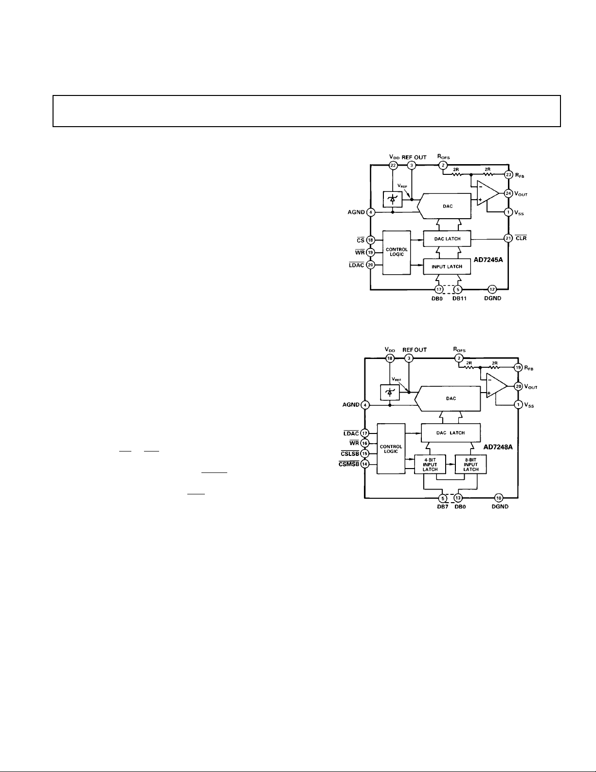
GENERAL DESCRIPTION
The AD7245A/AD7248A is an enhanced version of the industry
standard AD7245/AD7248. Improvements include operation
from 12 V to 15 V supplies, a ± 1/2 LSB linearity grade, faster
interface times and better full scale and reference variations with
V
DD
. Additional features include extended temperature range
operation for commercial and industrial grades.
The AD7245A/AD7248A is a complete, 12-bit, voltage output,
digital-to-analog converter with output amplifier and Zener volt-
age reference on a monolithic CMOS chip. No external user
trims are required to achieve full specified performance.
Both parts are microprocessor compatible, with high speed data
latches and double-buffered interface logic. The AD7245A ac-
cepts 12-bit parallel data which is loaded into the input latch on
the rising edge of
CS or WR. The AD7248A has an 8-bit wide
data bus with data loaded to the input latch in two write opera-
tions. For both parts, an asynchronous
LDAC signal transfers
data from the input latch to the DAC latch and updates the ana-
log output. The AD7245A also has a CLR signal on the DAC latch
which allows features such as power-on reset to be implemented.
The on-chip 5 V buried Zener diode provides a low noise, tem-
perature compensated reference for the DAC. For single supply
operation, two output ranges of 0 V to +5 V and 0 V to +10 V
are available, while these two ranges plus an additional ±5 V
range are available with dual supplies. The output amplifiers are
capable of developing +10 V across a 2 kΩ load to GND.
The AD7245A/AD7248A is fabricated in linear compatible
CMOS (LC
2
MOS), an advanced, mixed technology process that
combines precision bipolar circuits with low power CMOS logic.
The AD7245A is available in a small, 0.3" wide, 24-pin DIP
and
DACPORT is a registered trademark of Analog Devices, Inc.
AD7245A FUNCTIONAL BLOCK DIAGRAM
AD7248A FUNCTIONAL BLOCK DIAGRAM
SOIC and in 28-terminal surface mount packages. The
AD7248A is packaged in a small, 0.3" wide, 20-pin DIP and
SOIC and in 20-terminal surface mount packages.
PRODUCT HIGHLIGHTS
1. The AD7245A/AD7248A is a 12-bit DACPORT
®
on a single
chip. This single chip design and small package size offer
considerable space saving and increased reliability over
multichip designs.
2. The improved interface times on the part allows easy, direct
interfacing to most modern microprocessors.
3. The AD7245A/AD7248A features a wide power supply range
allowing operation from 12 V supplies.

A
2
B
2
T
2
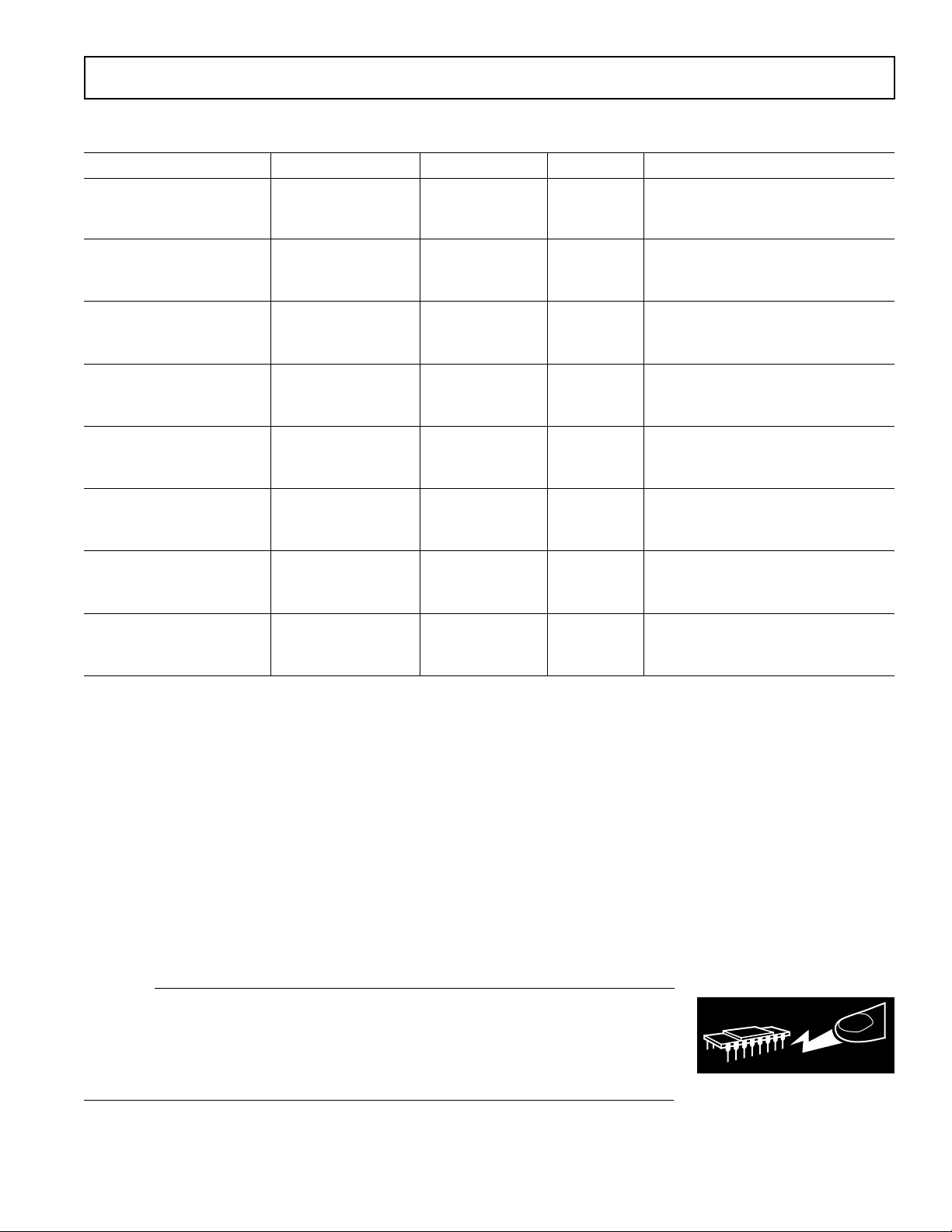
Parameter Version Version Version Units Test Conditions/Comments
STATIC PERFORMANCE
Resolution 12 12 12 Bits
Relative Accuracy @ +25°C
3
±3/4 ±1/2 ±1/2 LSB max
T
MIN
to T
MAX
±1 ±3/4 ±3/4 LSB max
T
MIN
to T
MAX
±1/2 LSB max V
DD
= 15 V ± 5%
Differential Nonlinearity
3
± 1 ±1 ±1 LSB max Guaranteed Monotonic
Unipolar Offset Error @ +25°C
3
±3 ±3 ±3 LSB max V
SS
= 0 V or –12 V to –15 V
4
T
MIN
to T
MAX
±5 ±5 ±5 LSB max Typical Tempco is ±3 ppm of FSR
5
/°C.
Bipolar Zero Error @ +25°C
3
±3 ±2 ±2 LSB max R
OFS
connected to REF OUT; V
SS
= –12 V to –15 V
4
T
MIN
to T
MAX
±5 ±4 ±4 LSB max Typical Tempco is ±3 ppm of FSR
5
/°C.
DAC Gain Error
3, 6
±2 ±2 ±2 LSB max
Full-Scale Output Voltage Error
7
@ +25°C
±0.2 ± 0.2 ±0.2 % of FSR max V
DD
= +15 V
∆Full Scale/∆V
DD
± 0.06 ± 0.06 ± 0.06 % of FSR/V max V
DD
= +12 V to +15 V
4
∆Full Scale/∆V
SS
± 0.01 ±0.01 ±0.01 % of FSR/V max V
SS
= –12 V to –15 V
4
Full-Scale Temperature Coefficient
8
± 30 ±30 ± 40
ppm of FSR/°C max
V
DD
= +15 V
REFERENCE OUTPUT
REF OUT @ +25°C 4.99/5.01 4.99/5.01 4.99/5.01 V min/V max V
DD
= +15 V
∆REF OUT/∆V
DD
2 2 2 mV/V max V
DD
= +12 V to +15 V
4
Reference Temperature Coefficient ±25 ±25 ±35 ppm/°C typ
Reference Load Change
(∆REF OUT vs. ∆I) –1 –1 –1 mV max Referenee Load Current Change (0–100 µA)
DIGITAL INPUTS
Input High Voltage, V
INH
2.4 2.4 2.4 V min
Input Low Voltage, V
INL
0.8 0.8 0.8 V max
Input Current, I
IN
±10 ± 10 ±10 µA max V
IN
= 0 V to V
DD
Input Capacitance
9
8 8 8 pF max
ANALOG OUTPUTS
Output Range Resistors 15/30 15/30 15/30 kΩ min/kΩ max
Output Voltage Ranges
10
+5, +10 +5, +10 +5, +10 V V
SS
= 0 V; Pin Strappable
Output Voltage Ranges
10
+5, +10, +5, +10, +5, +10, V
SS
= –12 V to –15 V;
4
Pin Strappable
±5 ±5 ±5V
DC Output Impedance 0.5 0.5 0.5 Ω typ
AC CHARACTERISTICS
9
Voltage Output Settling Time Settling Time to Within ±1/2 LSB of Final Value
Positive Full-Scale Change 7 7 10 µs max DAC Latch All 0s to All 1s
Negative Full-Scale Change 7 7 10 µs max DAC Latch All 1s to All 0s; V
SS
= –12 V to –15 V
4
Output Voltage Slew Rate 2 2 1.5 V/µs min
Digital Feedthrough
3
10 10 10 nV-s typ
Digital-to-Analog Glitch Impulse 30 30 30 nV-s typ
POWER REQUIREMENTS
V
DD
+10.8/ +11.4/ +11.4/ V min/ For Specified Performance Unless Otherwise Stated
+16.5 +15.75 +15.75 V max
V
SS
–10.8/ –11.4/ –11.4/ V min/ For Specified Performance Unless Otherwise Stated
–16.5 –15.75 –15.75 V max
I
DD
@ +25°C 9 9 9 mA max Output Unloaded; Typically 5 mA
T
MlN
to T
MAX
10 10 12 mA max Output Unloaded
I
SS
(Dual Supplies) 3 3 5 mA max Output Unloaded; Typically 2 mA
NOTES
1
Power supply tolerance is ±10% for A Version and ±5% for B and T Versions.
2
Temperature ranges are as follows: A/B Versions; –40°C to +85°C; T Version; –55°C to +125°C.
3
See Terminology.
4
With appropriate power supply tolerances.
5
FSR means Full-Scale Range and is 5 V for the 0 V to +5 V output range and 10 V for both the 0 V to +10 V and ±5 V output ranges.
6
This error is calculated with respect to the reference voltage and is measured after the offset error has been allowed for.
7
This error is calculated with respect to an ideal 4.9988 V on rhe 0 V to +5 V and ±5 V ranges; it is calculated with respect to an ideal 9.9976 V on the
0 V to +10 V range. It includes the effects of internal voltage reference, gain and offset errors.
8
Full-Scale TC = ∆FS/∆T, where ∆FS is the full-scale change from T
A
= +25°C to T
MIN
or T
MAX
.
9
Sample tested at +25°C to ensure compliance.
10
0 V to +10 V output range is available only when V
DD
≥ +14.25 V.
Specifications subject to change without notice.
AD7245A/AD7248A–SPECIFICATIONS
REV. A
–2–
(V
DD
= +12 V to +15 V,
1
V
SS
= O V or –12 V to –15 V,
1
AGND = DGND = O V, R
L
= 2 kV, C
L
= 1OO pF. All specifications T
MIN
to T
MAX
unless otherwise noted.)
AD7245A/AD7248A
REV. A
–3–
SWITCHING CHARACTERISTICS
1
(V
DD
= +12 V to +15 V;
2
V
SS
= O V or –12 V to –15 V;
2
See Figures 5 and 7.)
Parameter A, B Versions T Version Units Conditions
t
1
@ +25°C 55 55 ns typ Chip Select Pulse Width
T
MIN
to T
MAX
80 100 ns min
t
2
@ +25°C 40 40 ns typ Write Pulse Width
T
MIN
to T
MAX
80 100 ns min
t
3
@ +25°C 0 0 ns min Chip Select to Write Setup Time
T
MIN
to T
MAX
0 0 ns min
t
4
@ +25°C 0 0 ns min Chip Select to Write Hold Time
T
MIN
to T
MAX
0 0 ns min
t
5
@ +25°C 40 40 ns typ Data Valid to Write Setup Time
T
MIN
to T
MAX
80 80 ns min
t
6
@ +25°C 10 10 ns min Data Valid to Write Hold Time
T
MIN
to T
MAX
10 10 ns min
t
7
@ +25°C 40 40 ns typ Load DAC Pulse Width
T
MIN
to T
MAX
80 100 ns min
t
8
(AD7245A only)
@ +25°C 40 40 ns typ Clear Pulse Width
T
MIN
to T
MAX
80 100 ns min
NOTES
1
Sample tested at +25°C to ensure compliance.
2
Power supply tolerance is ±10% for A Version and ±5% for B and T Versions.
ABSOLUTE MAXIMUM RATINGS
1
V
DD
to AGND . . . . . . . . . . . . . . . . . . . . . . . . .–0.3 V to +17 V
V
DD
to DGND . . . . . . . . . . . . . . . . . . . . . . . . .–0.3 V to +17 V
V
DD
to V
SS
. . . . . . . . . . . . . . . . . . . . . . . . . . . .–0.3 V to +34 V
AGND to DGND . . . . . . . . . . . . . . . . . . . . . . . . .–0.3 V, V
DD
Digital Input Voltage to DGND . . . . . . . . –0.3 V, V
DD
+0.3 V
V
OUT
to AGND
2
. . . . . . . . . . . . . . . . . . . . . . . . . . . . V
SS
, V
DD
V
OUT
to V
SS
2
. . . . . . . . . . . . . . . . . . . . . . . . . . . . . 0 V, +24 V
V
OUT
to V
DD
2
. . . . . . . . . . . . . . . . . . . . . . . . . . . . . . –32 V, 0 V
REF OUT
2
to AGND . . . . . . . . . . . . . . . . . . . . . . . . 0 V, V
DD
Power Dissipation (Any Package) to +75°C . . . . . . . . 450 mW
Derates above +75°C by . . . . . . . . . . . . . . . . . . . . 6 mW/°C
Operating Temperature
Commercial (A, B Versions) . . . . . . . . . . . –40°C to +85°C
Extended (S Version) . . . . . . . . . . . . . . . –55°C to +125°C
Storage Temperature . . . . . . . . . . . . . . . . . . –65°C to +150°C
Lead Temperature (Soldering, 10 secs) . . . . . . . . . . . . +300°C
NOTES
1
Stresses above those listed under “Absolute Maximum Ratings” may cause per-
manent damage to the device. This is a stress rating only and functional opera-
tion of the device at these or any other conditions above those listed in the
operational sections of this specification is not implied. Exposure to absolute
maximum rating conditions for extended periods may affect device reliability.
2
The output may be shorted to voltages in this range provided the power dissipa-
tion of the package is not exceeded. V
OUT
short circuit current is typically
80 mA.
WARNING!
ESD SENSITIVE DEVICE
CAUTION
ESD (electrostatic discharge) sensitive device. Electrostatic charges as high as 4000 V readily
accumulate on the human body and test equipment and can discharge without detection.
Although the AD7245A/AD7248A features proprietary ESD protection circuitry, permanent
damage may occur on devices subjected to high energy electrostatic discharges. Therefore,
proper ESD precautions are recommended to avoid performance degradation or loss of function-
ality.
AD7245A/AD7248A
REV. A
–4–
DAC GAIN ERROR
DAC Gain Error is a measure of the output error between an
ideal DAC and the actual device output with all 1s loaded after
offset error has been allowed for. It is, therefore defined as:
Measured Value—Offset—Ideal Value
where the ideal value is calculated relative to the actual refer-
ence value.
UNIPOLAR OFFSET ERROR
Unipolar Offset Error is a combination of the offset errors of the
voltage mode DAC and the output amplifier and is measured
when the part is configured for unipolar outputs. It is present
for all codes and is measured with all 0s in the DAC register.
BIPOLAR ZERO OFFSET ERROR
Bipolar Zero Offset Error is measured when the part is config-
ured for bipolar output and is a combination of errors from the
DAC and output amplifier. It is present for all codes and is
measured with a code of 2048 (decimal) in the DAC register.
SINGLE SUPPLY LINEARITY AND GAIN ERROR
The output amplifier of the AD7245A/AD7248A can have a
true negative offset even when the part is operated from a single
positive power supply. However, because the lower supply rail
to the part is 0 V, the output voltage cannot actually go nega-
tive. Instead the output voltage sits on the lower rail and this re-
sults in the transfer function shown. This is an offset effect and
the transfer function would have followed the dotted line if the
output voltage could have gone negative. Normally, linearity is
measured after offset and full scale have been adjusted or al-
lowed for. On the AD7245A/AD7248A the negative offset is al-
lowed for by calculating the linearity from the code which the
amplifier comes off the lower rail. This code is given by the
negative offset specification. For example, the single supply lin-
earity specification applies between Code 3 and Code 4095 for
the 25°C specification and between Code 5 and Code 4095 over
the T
MIN
to T
MAX
temperature range. Since gain
error is also
measured after offset has been allowed for, it is calculated between
the same codes as the linearity error. Bipolar linearity and gain er-
ror are measured between Code 0 and Code 4095.
OUTPUT
VOLTAGE
NEGATIVE
OFFSET
DAC CODE
0V
{
TERMINOLOGY
RELATIVE ACCURACY
Relative Accuracy, or end-point nonlinearity, is a measure of the
actual deviation from a straight line passing through the end-
points of the DAC transfer function. It is measured after allow-
ing for zero and full scale and is normally expressed in LSBs or
as a percentage of full-scale reading.
DIFFERENTIAL NONLINEARITY
Differential Nonlinearity is the difference between the measured
change and the ideal 1 LSB change between any two adjacent
codes. A specified differential nonlinearity of ± 1 LSB max over
the operating temperature range ensures monotonicity.
DIGITAL FEEDTHROUGH
Digital Feedthrough is the glitch impulse injected from the digi-
tal inputs to the analog output when the inputs change state. It
is measured with
LDAC high and is specified in nV-s.
AD7245A ORDERING GUIDE
Temperature Relative Package
Model
l
Range Accuracy Option
2
AD7245AAN –40°C to +85°C ±3/4 LSB N-24
AD7245ABN –40°C to +85°C ±1/2 LSB N-24
AD7245AAQ –40°C to +85°C ±3/4 LSB Q-24
AD7245ATQ
3
–55°C to +125°C ±3/4 LSB Q-24
AD7245AAP –40°C to +85°C ±3/4 LSB P-28A
AD7245AAR –40°C to +85°C ±3/4 LSB R-24
AD7245ABR –40°C to +85°C ±1/2 LSB R-24
AD7245ATE
3
–55°C to +125°C ±3/4 LSB E-28A
NOTES
1
To order MIL-STD-883, Class B. processed parts, add /883B to part number.
Contact our local sales office for military data sheet and availability.
2
E = Leadless Ceramic Chip Carrier; N = Plastic DIP; P = Plastic Leaded Chip
Carrier; Q = Cerdip; R = SOIC.
3
This grade will be available to /883B processing only.
AD7248A ORDERING GUIDE
Temperature Relative Package
Model
l
Range Accuracy Option
2
AD7248AAN –40°C to +85°C ±3/4 LSB N-20
AD7248ABN –40°C to +85°C ±1/2 LSB N-20
AD7248AAQ –40°C to +85°C ±3/4 LSB Q-20
AD7248ATQ
3
–55°C to +125°C ±3/4 LSB Q-20
AD7248AAP –40°C to +85°C ±3/4 LSB P-20A
AD7248AAR –40°C to +85°C ±3/4 LSB R-20
AD7248ABR –40°C to +85°C ±1/2 LSB R-20
NOTES
1
To order MIL-STD-883, Class B, processed parts, add /883B to part number.
Contact our local sales office for military data sheet and availability.
2
N = Plastic DIP; P = Plastic Leaded Chip Carrier; Q = Cerdip; R = SOIC.
3
This grade will be available to /883B processing only.
AD7245A/AD7248A
REV. A
–5–
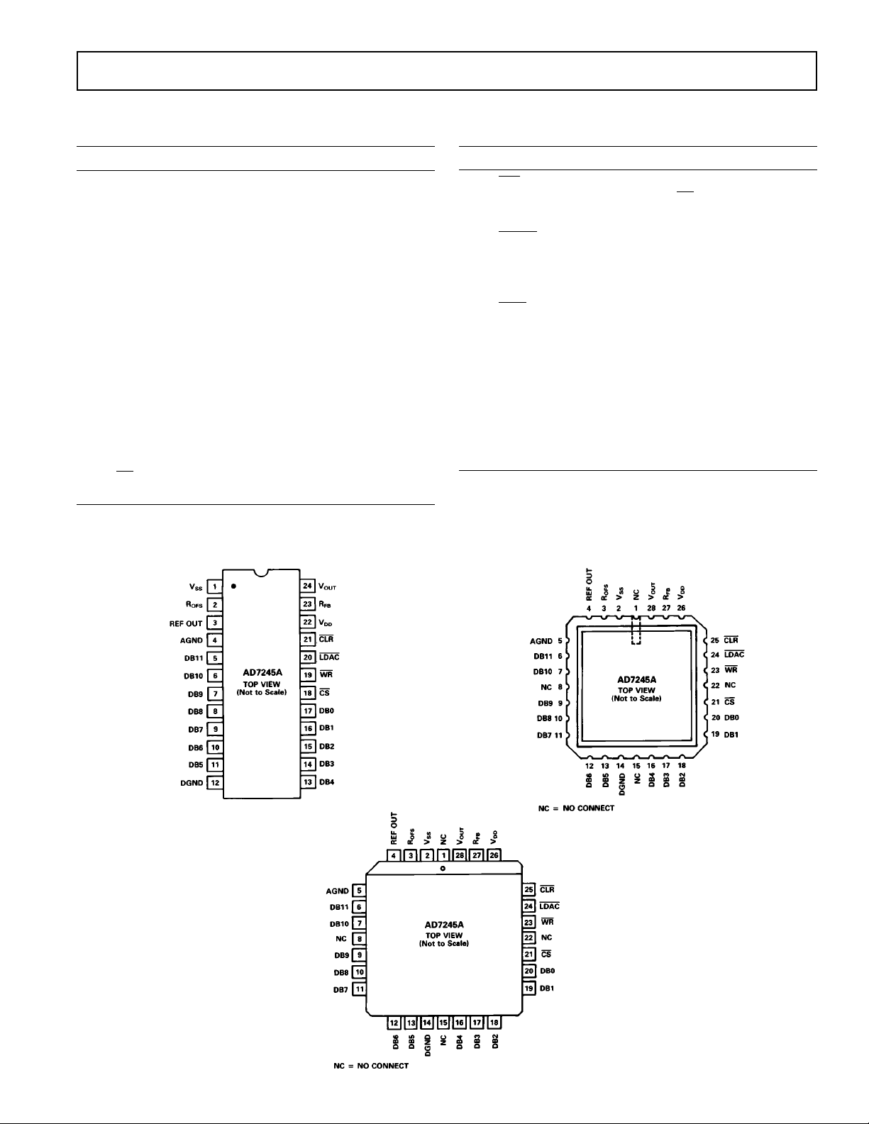
AD7248A PIN FUNCTION DESCRIPTION
(DIP PIN NUMBERS)
Pin Mnemonic Description
lV
SS
Negative Supply Voltage (0 V for single
supply operation).
2R
OFS
Bipolar Offset Resistor. This provides
access to the on-chip application resistors
and allows different output voltage ranges.
3 REF OUT Reference Output. The on-chip reference
is provided at this pin and is used when
configuring the part for bipolar outputs.
4 AGND Analog Ground.
5 DB11 Data Bit 11. Most Significant Bit (MSB).
6-11 DB10-DB5 Data Bit 10 to Data Bit 5.
12 DGND Digital Ground.
13-16 DB4-DB1 Data Bit 4 to Data Bit 1.
17 DB0 Data Bit 0. Least Significant Bit (LSB).
18
CS Chip Select Input (Active LOW). The de-
vice is selected when this input is active.
Pin Mnemonic Description
19
WR Write Input (Active LOW). This is used in
conjunction with
CS to write data into the
input latch of the AD7245A.
20
LDAC Load DAC Input (Active LOW). This is
an asynchronous input which when active
transfers data from the input latch to the
DAC latch.
21
CLR Clear Input (Active LOW). When this in-
put is active the contents of the DAC latch
are reset to all 0s.
22 V
DD
Positive Supply Voltage.
23 R
FB
Feedback Resistor. This allows access to
the amplifier’s feedback loop.
24 V
OUT
Output Voltage. Three different output
voltage ranges can be chosen: 0 V to +5 V,
0 V to +10 V or –5 V to +5 V.
PLCC
AD7245A PIN CONFIGURATIONS
DIP and SOIC LCCC
Loading...