


AD724-EB
Table of contents
 Loading...
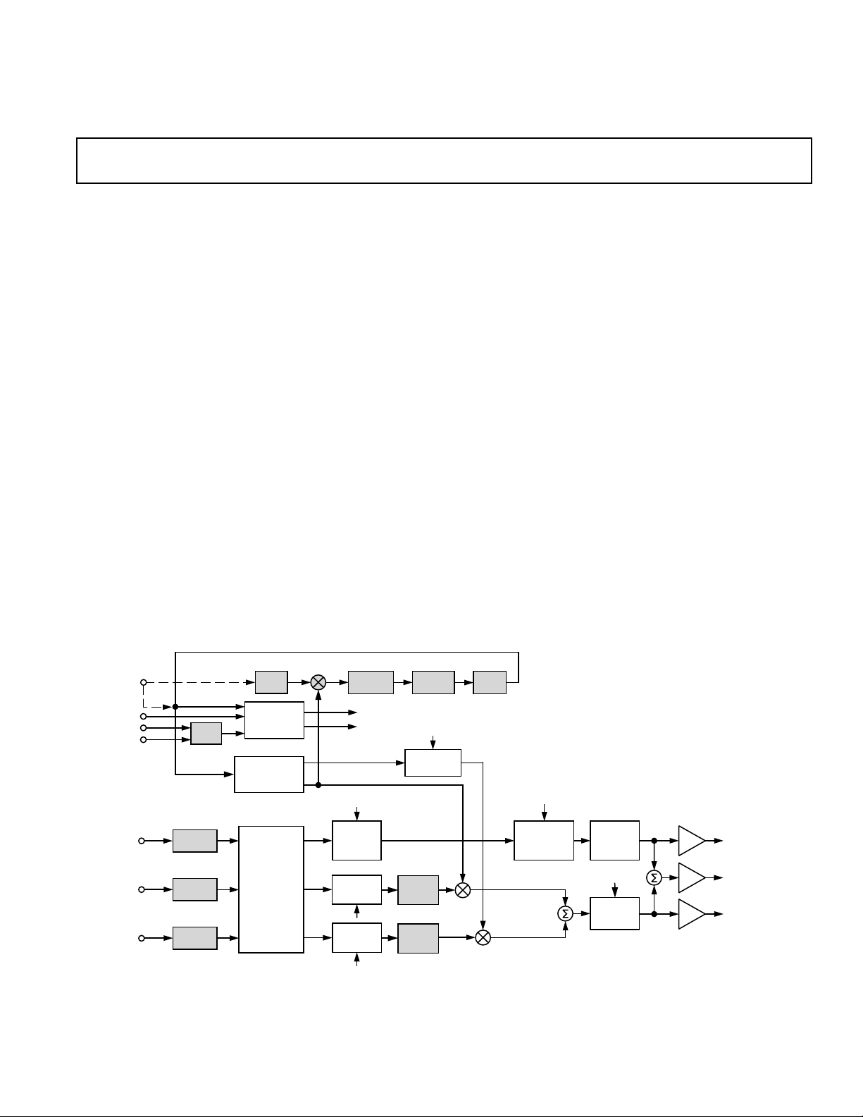
a
RGB to NTSC/PAL Encoder
AD724
FEATURES
Low Cost, Integrated Solution
+5 V Operation
Accepts FSC Clock or Crystal, or 4FSC Clock
Composite Video and Separate Y/C (S-Video) Outputs
Luma and Chroma Outputs Are Time Aligned
Minimal External Components:
No External Filters or Delay Lines Required
Onboard DC Clamp
Accepts Either HSYNC & VSYNC or CSYNC
Phase Lock to External Subcarrier
Drives 75 ⍀ Reverse-Terminated Loads
Logic Selectable NTSC or PAL Encoding Modes
Compact 16-Lead SOIC
APPLICATIONS
RGB to NTSC or PAL Encoding
PRODUCT DESCRIPTION
The AD724 is a low cost RGB to NTSC/PAL Encoder that
converts red, green and blue color component signals into their
corresponding luminance (baseband amplitude) and chromi-
nance (subcarrier amplitude and phase) signals in accordance
with either NTSC or PAL standards. These two outputs are also
combined to provide composite video output. All three outputs can
simultaneously drive 75 Ω, reverse-terminated cables. All logi-
cal inputs are TTL, 3 V and 5 V CMOS compatible. The chip
operates from a single +5 V supply. No external delay lines or
filters are required. The AD724 may be powered down when
not in use.
The AD724 accepts either FSC or 4FSC clock. When a clock is
not available, a low cost parallel-resonant crystal (3.58 MHz
(NTSC) or 4.43 MHz (PAL)) and the AD724’s on-chip oscilla-
tor generate the necessary subcarrier clock. The AD724 also
accepts the subcarrier clock from an external video source.
The interface to graphics controllers is simple: an on-chip logic
“XNOR” accepts the available vertical (VSYNC) and horizon-
tal sync (HSYNC) signals and creates the composite sync
(CSYNC) signal on-chip. If available, the AD724 will also
accept a standard CSYNC signal by connecting VSYNC to
Logic HI and applying CSYNC to the HSYNC pin. The
AD724 contains decoding logic to identify valid horizontal sync
pulses for correct burst insertion.
Delays in the U and V chroma filters are matched by an on-chip
sampled-data delay line in the Y signal path. To prevent alias-
ing, a prefilter at 5 MHz is included ahead of the delay line and
a post-filter at 5 MHz is added after the delay line to suppress
harmonics in the output. These low-pass filters are optimized
for minimum pulse overshoot. The overall luma delay, relative
to chroma, has been designed to be time aligned for direct input to
a television’s baseband. The AD724 comes in a space-saving
SOIC and is specified for the 0°C to +70°C commercial tem-
perature range.
FUNCTIONAL BLOCK DIAGRAM
4FSC
PHASE
DETECTOR
LOOP
FILTER
4FSC
FSC
SUB-
CARRIER
NTSC/PAL
HSYNC
VSYNC
BURST
NTSC/PAL
FSC 90
°
FSC 0
°
SC 90
°
/270
°
FSC
CSYNC
CSYNC
DC
CLAMP
RED
GREEN
BLUE
RGB-TO-YUV
ENCODING
MATRIX
CSYNC
Y
U
V
4-POLE
LPF
4-POLE
LPF
BALANCED
MODULATORS
4-POLE
LPF
NTSC/PAL
SAMPLED-
DATA
DELAY LINE
X2
X2
X2
LUMINANCE
OUTPUT
COMPOSITE
OUTPUT
CHROMINANCE
OUTPUT
U
CLAMP
CLOCK
AT 8FSC
4FSC
VCO
CHARGE
PUMP
XOSC
XNOR
SYNC
SEPARATOR
QUADRATURE
+4
DECODER
BURST
V
CLAMP
±180°
(PAL ONLY)
2-POLE
LP POST-
FILTER
3-POLE
LP PRE-
FILTER
4FSC
DC
CLAMP
DC
CLAMP
REV. A
Information furnished by Analog Devices is believed to be accurate and
reliable. However, no responsibility is assumed by Analog Devices for its
use, nor for any infringements of patents or other rights of third parties
which may result from its use. No license is granted by implication or
otherwise under any patent or patent rights of Analog Devices.
One Technology Way, P.O. Box 9106, Norwood, MA 02062-9106, U.S.A.
Tel: 781/329-4700 World Wide Web Site: http://www.analog.com
Fax: 781/326-8703 © Analog Devices, Inc., 1999

AD724–SPECIFICA TIONS
REV. A
–2–
(Unless otherwise noted, V
S
= +5, T
A
= +25ⴗC, using FSC synchronous clock. All loads are
150 ⍀ ⴞ 5% at the IC pins. Outputs are measured at the 75 ⍀ reverse terminated load.)
Parameter Conditions Min Typ Max Units
SIGNAL INPUTS (RIN, GIN, BIN)
Input Amplitude Full Scale 714 mV p-p
Black Level
1
0.8 V
Input Resistance
2
RIN, GIN, BIN 1 MΩ
Input Capacitance 5pF
LOGIC INPUTS (HSYNC, VSYNC, FIN, ENCD, STND, SELECT) CMOS Logic Levels
Logic LO Input Voltage 1V
Logic HI Input Voltage 2V
Logic LO Input Current (DC) <1 µA
Logic HI Input Current (DC) <1 µA
VIDEO OUTPUTS
3
Luminance (LUMA)
Roll-Off @ 5 MHz NTSC –7 dB
PAL –6 dB
Gain Error –15 –3 +15 %
Nonlinearity ±0.3 %
Sync Level NTSC 243 286 329 mV
PAL 300 mV
DC Black Level 1.3 V
Chrominance (CRMA)
Bandwidth NTSC 3.6 MHz
PAL 4.4 MHz
Color Burst Amplitude NTSC 170 249 330 mV p-p
PAL 288 mV
Color Signal to Burst Ratio Error
4
±5%
Color Burst Width NTSC 2.51 µs
PAL 2.28 µs
Phase Error
5
±3 Degrees
DC Black Level 2.0 V
Chroma Feedthrough R, G, B = 0 15 40 mV p-p
Composite (COMP)
Absolute Gain Error With Respect to Luma –5 ±15 %
Differential Gain With Respect to Chroma 0.5 %
Differential Phase With Respect to Chroma 2.0 Degrees
DC Black Level 1.5 V
Chroma/Luma Time Alignment 0ns
POWER SUPPLIES
Recommended Supply Range Single Supply +4.75 +5.25 V
Quiescent Current—Encode Mode
6
33 42 mA
Quiescent Current—Power Down 1 mA
NOTES
1
R, G, and B signals are inputted via an external ac coupling capacitor.
2
Except during dc restore period (back porch clamp).
3
All outputs measured at a 75 Ω reverse-terminated load; ac voltages at the IC output pins are twice those specified here.
4
Ratio of chroma amplitude to burst amplitude, difference from ideal.
5
Difference between ideal color-bar phases and the actual values.
6
Driving the logic inputs with VOH < 4 V will increase static supply current approximately 150 µA per input.
Specifications are subject to change without notice.
AD724
REV. A
–3–
ORDERING GUIDE
Temperature Package Package
Model Range Description Option
AD724JR 0°C to +70°C 16-Lead SOIC R-16
AD724JR-REEL 0°C to +70°C 16-Lead SOIC R-16
AD724JR-REEL7 0°C to +70°C 16-Lead SOIC R-16
AD724-EB Evaluation Board
ABSOLUTE MAXIMUM RATINGS*
Supply Voltage, APOS to AGND . . . . . . . . . . . . . . . . . . +6 V
Supply Voltage, DPOS to DGND . . . . . . . . . . . . . . . . . . +6 V
AGND to DGND . . . . . . . . . . . . . . . . . . . . . –0.3 V to +0.3 V
Inputs . . . . . . . . . . . . . . . . . . . DGND – 0.3 to DPOS + 0.3 V
Internal Power Dissipation . . . . . . . . . . . . . . . . . . . . . .800 mW
Operating Temperature Range . . . . . . . . . . . . . 0°C to +70°C
Storage Temperature Range . . . . . . . . . . . . .–65°C to +125°C
Lead Temperature Range (Soldering 30 sec) . . . . . . . . +230°C
*Stresses above those listed under Absolute Maximum Ratings may cause perma-
nent damage to the device. This is a stress rating only; functional operation of the
device at these or any other conditions above those indicated in the operational
section of this specification is not implied. Exposure to absolute maximum rating
conditions for extended periods may affect device reliability.
Thermal Characteristics: 16-Lead SOIC Package: θ
JA
= 100°C/W.
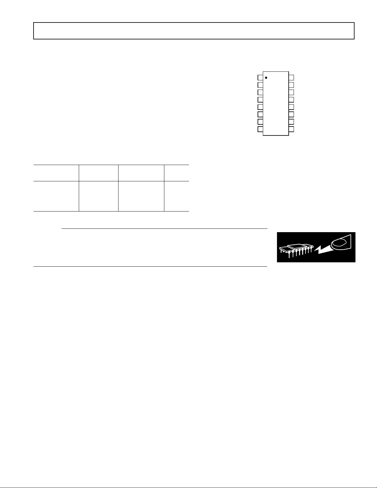
PIN CONFIGURATION
16-Lead Wide Body (SOIC)
(R-16)
TOP VIEW
(Not to Scale)
16
15
14
13
12
11
10
9
1
2
3
4
5
6
7
8
STND
AGND
FIN
APOS
ENCD
RIN
GIN
BIN
HSYNC
VSYNC
DPOS
DGND
SELECT
LUMA
COMP
CRMA
AD724
CAUTION
ESD (electrostatic discharge) sensitive device. Electrostatic charges as high as 4000 V readily
accumulate on the human body and test equipment and can discharge without detection.
Although the AD724 features proprietary ESD protection circuitry, permanent damage may
occur on devices subjected to high energy electrostatic discharges. Therefore, proper ESD
precautions are recommended to avoid performance degradation or loss of functionality.
WARNING!
ESD SENSITIVE DEVICE
REV. A
–4–
AD724
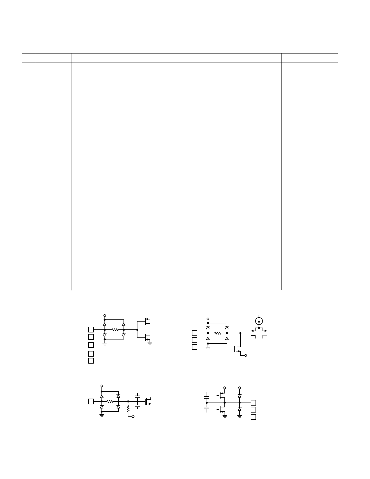
PIN FUNCTION DESCRIPTIONS
Pin Mnemonic Description Equivalent Circuit
1 STND A Logical HIGH input selects NTSC encoding. Circuit A
A Logical LOW input selects PAL encoding.
CMOS/TTL Logic Levels.
2 AGND Analog Ground Connection.
3 FIN FSC clock or parallel-resonant crystal, or 4FSC clock input. Circuit B
For NTSC: 3.579 545 MHz or 14.318 180 MHz.
For PAL: 4.433 619 MHz or 17.734 480 MHz.
CMOS/TTL Logic Levels for subcarrier clocks.
4 APOS Analog Positive Supply (+5 V ± 5%).
5 ENCD A Logical HIGH input enables the encode function. Circuit A
A Logical LOW input powers down chip when not in use.
CMOS/TTL Logic Levels.
6 RIN Red Component Video Input. Circuit C
0 to 714 mV AC-Coupled.
7 GIN Green Component Video Input. Circuit C
0 to 714 mV AC-Coupled.
8 BIN Blue Component Video Input. Circuit C
0 to 714 mV AC-Coupled.
9 CRMA Chrominance Output.* Circuit D
Approximately 1.8 V peak-to-peak for both NTSC and PAL.
10 COMP Composite Video Output.* Circuit D
Approximately 2.5 V peak-to-peak for both NTSC and PAL.
11 LUMA Luminance plus SYNC Output.* Circuit D
Approximately 2 V peak-to-peak for both NTSC and PAL.
12 SELECT A Logical LOW input selects the FSC operating mode. Circuit A
A Logical HIGH input selects the 4FSC operating mode.
CMOS/TTL Logic Levels.
13 DGND Digital Ground Connections.
14 DPOS Digital Positive Supply (+5 V ± 5%).
15 VSYNC Vertical Sync Signal (if using external CSYNC set at > +2 V). CMOS/TTL Logic Levels. Circuit A
16 HSYNC Horizontal Sync Signal (or CSYNC signal). CMOS/TTL Logic Levels. Circuit A
*The Luminance, Chrominance and Composite Outputs are at twice normal levels for driving 75 Ω reverse-terminated lines.
5
1
12
15
16
DPOS
DGND
3
V
BIAS
DPOS
DGND
7
V
CLAMP
6
8
DPOS
DGND
10
9
11
APOS
AGND
DGND
DPOS
Circuit B Circuit D
Equivalent Circuits
Circuit A Circuit C
REV. A
–5–
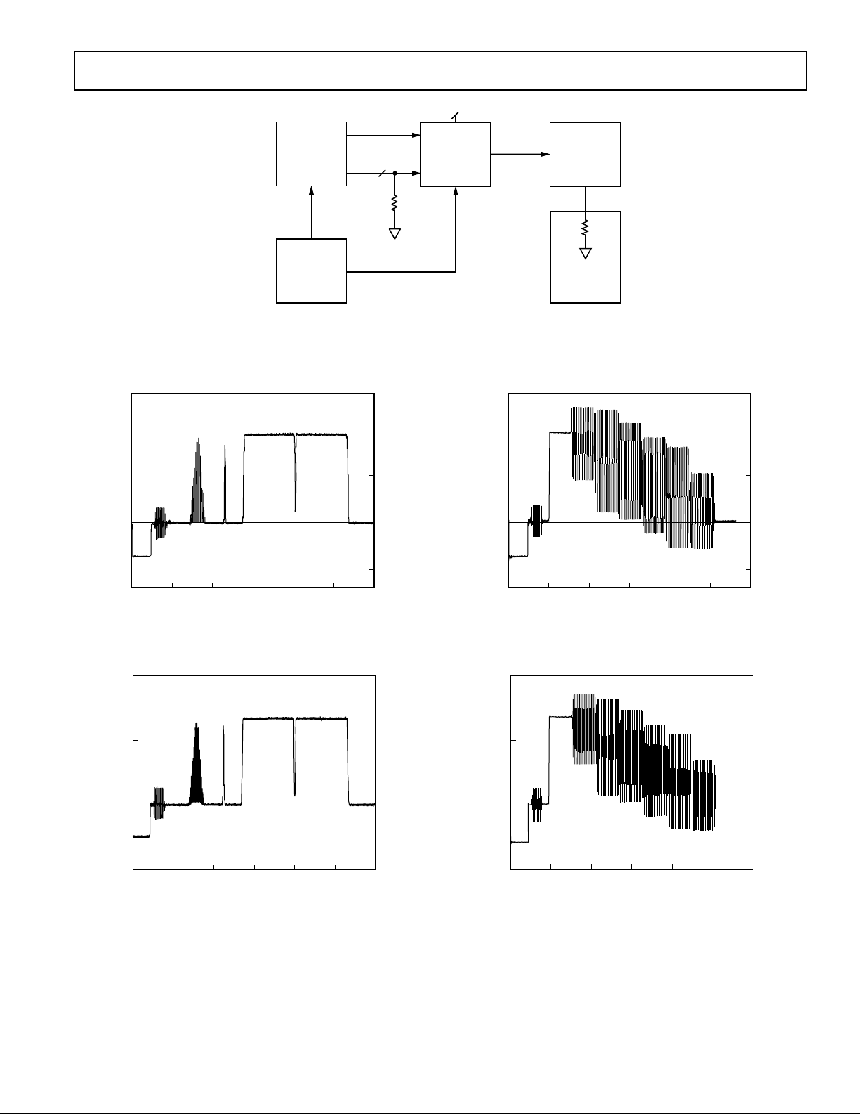
APL = 49.8%
525 LINE NTSC NO FILTERING
SLOW CLAMP TO 0.00V
@ 6.63ms
ms
06010 20 30 40 50
SYNCHRONOUS SYNC = SOURCE
FRAMES SELECTED : 1 2
IRE
1.0
0.5
–0.5
0.0
100
50
0
–50
VOLTS
Figure 2. Modulated Pulse and Bar, NTSC
ms
1.0
0.5
–0.5
06010 20 30 40 50
0.0
APL = 50.0%
625 LINE PAL NO FILTERING
SLOW CLAMP TO 0.00V @ 6.72ms
ASYNCHRONOUS SYNC = SOURCE
FRAMES SELECTED : 1 2 3 4
VOLTS
Figure 3. Modulated Pulse and Bar, PAL
RGB
3
75V
75V
COMPOSITE
VIDEO
COMPOSITE
SYNC
FSC
GENLOCK
TEKTRONIX
TSG 300
COMPONENT
VIDEO
WAVEFORM
GENERATOR
AD724
RGB TO
NTSC/PAL
ENCODER
TEKTRONIX
VM700A
WAVEFORM
MONITOR
TEKTRONIX
1910
COMPOSITE
VIDEO
WAVEFORM
GENERATOR
SONY
MONITOR
MODEL
1342
+5V
FIN
Figure 1. Evaluation Setup
T ypical Characteristics–AD724
IRE
ms
1.0
0.5
–0.5
06010 20 30 40 50
0.0
APL = 50.8%
525 LINE NTSC NO FILTERING
SLOW CLAMP TO 0.00V @ 6.63ms
PRECISION MODE OFF
SYNCHRONOUS SYNC = SOURCE
FRAMES SELECTED : 1 2
100
50
0
–50
VOLTS
Figure 4. 100% Color Bars, NTSC
ms
1.0
0.5
–0.5
06010 20 30 40 50
0.0
VOLTS
APL = 50.6%
625 LINE PAL NO FILTERING
SLOW CLAMP TO 0.00V @ 6.72
m
s
ASYNCHRONOUS SYNC = SOURCE
FRAMES SELECTED : 1 2 3 4
Figure 5. 100% Color Bars, PAL
Loading...