


 Loading...
Analog Devices ADV7120KST50, ADV7120KST30, ADV7120KP80, ADV7120KP50, ADV7120KP30 Datasheet
...a |
CMOS |
80 MHz, Triple 8-Bit Video DAC |
|
|
|
|
|
|
|
|
|
ADV7120 |
||||||
|
|
|
|
|
|
|
|
|
|
|
|
|
|
|
|
FEATURES |
|
|
|
|
|
FUNCTIONAL BLOCK DIAGRAM |
|
||||||||
80 MHz Pipelined Operation |
|
|
|
|
|
|
|
|
|
|
|
|
|
|
|
Triple 8-Bit D/A Converters |
|
|
|
|
|
VAA |
FS |
VREF |
|
||||||
RS-343A/RS-170 Compatible Outputs |
|
|
|
|
|
ADJUST |
|
||||||||
|
|
|
|
|
|
|
|
|
|
|
|
|
|
|
|
TTL Compatible Inputs |
|
|
|
|
|
|
|
|
|
REFERENCE |
|
||||
+5 V CMOS Monolithic Construction |
|
|
|
|
|
ADV7120 |
|
|
|||||||
|
|
|
|
|
|
|
AMPLIFIER |
|
|||||||
|
|
|
|
|
|
|
|
||||||||
40-Pin DIP or 44-Pin PLCC and 48-Lead TQFP |
CLOCK |
|
|
|
|
|
|
|
|
|
|
|
COMP |
||
|
|
|
|
|
|
|
|
|
|
|
|
||||
APPLICATIONS |
|
|
|
|
|
|
|
|
|
|
|
|
|
|
|
|
|
|
|
|
|
|
|
|
|
|
|
|
|
|
|
|
R0 |
|
|
|
|
8 |
RED |
8 |
|
|
|
|
|
|
|
High Resolution Color Graphics |
|
|
|
|
|
REGISTER |
DAC |
|
|
|
IOR |
||||
|
R7 |
|
|
|
|
|
|
|
|
||||||
|
|
|
|
|
|
|
|
|
|
|
|||||
CAE/CAD/CAM Applications |
|
|
|
|
|
|
|
|
|
|
|
|
|
|
|
Image Processing |
PIXEL |
G0 |
|
|
|
|
GREEN |
8 |
|
|
|
|
|
|
|
INPUT |
|
|
|
8 |
|
|
|
|
|
|
|||||
Instrumentation |
G7 |
|
|
|
REGISTER |
|
DAC |
|
IOG |
||||||
PORT |
|
|
|
|
|
|
|
|
|||||||
Video Signal Reconstruction |
|
|
|
|
|
|
|
|
|
|
|
|
|
|
|
Desktop Publishing |
|
B0 |
|
|
|
|
8 |
BLUE |
8 |
|
|
|
|
|
|
|
|
|
|
|
|
||||||||||
Direct Digital Synthesis (DDS) and I/Q Modulation |
|
|
|
|
|
|
REGISTER |
|
DAC |
|
IOB |
||||
|
B7 |
|
|
|
|
|
|
|
|
||||||
SPEED GRADES* |
|
|
|
|
|
|
|
|
|
|
|
|
|
|
|
|
|
|
|
|
|
|
|
|
|
|
|
|
|
|
|
|
|
|
|
|
|
|
|
|
|
|
|
|
|
|
|
|
|
|
|
|
|
|
|
|
|
|
|
|
|
|
|
80 MHz |
REF WHITE |
|
|
|
|
CONTROL |
|
|
|
|
|
|
|
||
50 MHz |
BLANK |
|
|
|
|
REGISTER |
|
SYNC |
|
ISYNC |
|||||
|
SYNC |
|
|
|
|
|
|
CONTROL |
|
||||||
30 MHz |
|
|
|
|
|
|
|
|
|
|
|
|
|
||
|
|
|
|
|
|
|
|
|
|
|
|
|
|
|
|
|
|
|
|
|
|
|
|
|
|
|
|
|
|
|
|
|
|
|
|
|
|
|
|
|
|
|
|
|
|
|
|
|
|
|
|
|
|
GND |
|
|
|
|
|
|
|
|
|
GENERAL DESCRIPTION
The ADV7120 (ADV®) is a digital to analog video converter on a single monolithic chip. The part is specifically designed for high resolution color graphics and video systems. It is also ideal for any high speed communications type applications requiring low cost, high speed DACs. It consists of three, high speed, 8-bit, video D/A converters (RGB); a standard TTL input interface and high impedance, analog output, current sources.
The ADV7120 has three separate, 8-bit, pixel input ports, one each for red, green and blue video data. Additional video input controls on the part include composite sync, blank and reference white. A single +5 V supply, an external 1.23 V reference and pixel clock input are all that are required to make the part operational.
The ADV7120 is capable of generating RGB video output signals, which are compatible with RS-343A and RS-170 video standards, without requiring external buffering.
The ADV7120 is fabricated in a +5 V CMOS process. Its monolithic CMOS construction ensures greater functionality with low power dissipation. The part is packaged in both a 0.6", 40-pin plastic DIP and a 44-pin plastic leaded (J-lead) chip carrier, PLCC. The ADV7120 is also available in a very small 48lead Thin Quad Flatpack (TQFP).
ADV is a registered trademark of Analog Devices, Inc.
*Speed grades up to 140 MHz are also available upon special request. Please contact Analog Devices or its representatives for further details.
PRODUCT HIGHLIGHTS
1.Fast video refresh rate, 80 MHz.
2.Compatible with a wide variety of high resolution color graphics video systems.
3.Guaranteed monotonic with a maximum differential nonlinearity of ±0.5 LSB. Integral nonlinearity is guaranteed to be a maximum of ±1 LSB.
REV. B
Information furnished by Analog Devices is believed to be accurate and reliable. However, no responsibility is assumed by Analog Devices for its use, nor for any infringements of patents or other rights of third parties which may result from its use. No license is granted by implication or otherwise under any patent or patent rights of Analog Devices.
One Technology Way, P.O. Box 9106, Norwood, MA 02062-9106, U.S.A. Tel: 617/329-4700 Fax: 617/326-8703
|
|
(VAA = +5 V 6 5%; VREF = +1.235 V; RL = 37.5 V, CL = 10 pF; RSET = 560 V. |
|
ADV7120–SPECIFICATIONS ISYNC connected to I0G. All Specifications TMIN to TMAX1 unless otherwise noted.) |
|||
|
|
|
|
Parameter |
All Versions |
Units |
Test Conditions/Comments |
|
|
|
|
STATIC PERFORMANCE |
|
|
|
Resolution (Each DAC) |
8 |
Bits |
|
Accuracy (Each DAC) |
±1 |
|
|
Integral Nonlinearity, INL |
LSB max |
|
|
Differential Nonlinearity, DNL |
±0.5 |
LSB max |
Guaranteed Monotonic |
Gray Scale Error |
±5 |
% Gray Scale max |
Max Gray Scale Current: IOG = (VREF* 12,082/RSET) mA |
|
|
|
IOR, IOB = (VREF* 8,627/RSET) mA |
Coding |
Binary |
|
|
|
|
|
|
DIGITAL INPUTS |
|
|
|
Input High Voltage, VINH |
2 |
V min |
|
Input Low Voltage, VINL |
0.8 |
V max |
|
Input Current, IIN |
± 1 |
μA max |
VIN = 0.4 V or 2.4 V |
Input Capacitance, CIN2 |
10 |
pF max |
|
ANALOG OUTPUTS |
|
|
|
Gray Scale Current Range |
15 |
mA min |
|
|
22 |
mA max |
|
Output Current |
|
|
|
White Level Relative to Blank |
17.69 |
mA min |
Typically 19.05 mA |
|
20.40 |
mA max |
|
White Level Relative to Black |
16.74 |
mA min |
Typically 17.62 mA |
|
18.50 |
mA max |
|
Black Level Relative to Blank |
0.95 |
mA min |
Typically 1.44 mA |
|
1.90 |
mA max |
|
Blank Level on IOR, IOB |
0 |
μA min |
Typically 5 μA |
|
50 |
μA max |
|
Blank Level on IOG |
6.29 |
mA min |
Typically 7.62 mA |
|
9.5 |
mA max |
|
Sync Level on IOG |
0 |
μA min |
Typically 5 μA |
|
50 |
μA max |
|
LSB Size |
69.1 |
μA typ |
|
DAC to DAC Matching |
5 |
% max |
Typically 2% |
Output Compliance, VOC |
–1 |
V min |
|
|
+1.4 |
V max |
|
2 |
100 |
kΩ typ |
|
Output Impedance, ROUT |
|
||
2 |
30 |
pF max |
IOUT = 0 mA |
Output Capacitance, COUT |
|||
VOLTAGE REFERENCE |
|
|
|
Voltage Reference Range, VREF |
1.14/1.26 |
V min/V max |
VREF = 1.235 V for Specified Performance |
Input Current, IVREF |
–5 |
mA typ |
|
POWER REQUIREMENTS |
|
|
|
VAA |
5 |
V nom |
|
IAA |
125 |
mA max |
Typically 80 mA: 80 MHz Parts |
|
100 |
mA max |
Typically 70 mA: 50 MHz & 35 MHz Parts |
Power Supply Rejection Ratio |
0.5 |
%/% max |
Typically 0.12%/%: f = 1 kHz, COMP = 0.1 μF |
Power Dissipation |
625 |
mW max |
Typically 400 mW: 80 MHz Parts |
|
500 |
mW max |
Typically 350 mW: 50 MHz & 30 MHz Parts |
|
|
|
|
DYNAMIC PERFORMANCE |
|
|
|
Glitch Impulse2, 3 |
50 |
pV secs typ |
|
DAC Noise2, 3, 4 |
200 |
pV secs typ |
|
Analog Output Skew |
2 |
ns max |
Typically 1 ns |
|
|
|
|
NOTES
1Temperature range (TMIN to TMIN); 0°C to +70°C. 2Sample tested at +25°C to ensure compliance.
3TTL input values are 0 to 3 volts, with input rise/fall times ≤3 ns, measured between the 10% and 90% points. Timing reference points at 50% for inputs and outputs. See timing notes in Figure 1.
4This includes effects due to clock and data feedthrough as well as RGB analog crosstalk.
Specifications subject to change without notice.
–2– |
REV. B |
|
|
|
|
|
|
ADV7120 |
|
|
|
|
|
|
|
TIMING CHARACTERISTICS1 |
(VAA = +5 V 6 5%; VREF = +1.235 V; RL = 37.5 V, CL = 10 pF; RSET = 560 V. |
|||||
ISYNC connected to IOG. All Specifications TMIN to TMAX2 unless otherwise noted.) |
||||||
|
|
|
|
|
|
|
Parameter |
80 MHz Version |
50 MHz Version |
30 MHz Version |
Units |
Conditions/Comments |
|
|
|
|
|
|
|
|
fMAX |
80 |
50 |
|
30 |
MHz max |
Clock Rate |
tl |
3 |
6 |
|
8 |
ns min |
Data & Control Setup Time |
t2 |
2 |
2 |
|
2 |
ns min |
Data & Control Hold Time |
t3 |
12.5 |
20 |
|
33.3 |
ns min |
Clock Cycle Time |
t4 |
4 |
7 |
|
9 |
ns min |
Clock Pulse Width High Time |
t5 |
4 |
7 |
|
9 |
ns min |
Clock Pulse Width Low Time |
t6 |
30 |
30 |
|
30 |
ns max |
Analog Output Delay |
|
20 |
20 |
|
20 |
ns typ |
|
t7 |
3 |
3 |
|
3 |
ns max |
Analog Output Rise/Fall Time |
t83 |
12 |
15 |
|
15 |
ns typ |
Analog Output Transition Time |
NOTES
1TTL input values are 0 to 3 volts, with input rise/fall times ≤3 ns, measured between the 10% and 90% points. Timing reference points at 50% for inputs and outputs. See timing notes in Figure 1.
2Temperature range (TMIN to TMAX): 0°C to +70°C 3Sample tested at +25°C to ensure compliance.
Specifications subject to change without notice.
|
t4 |
|
t5 |
|
|||
CLOCK |
|
|
|
|
|
||
|
|
|
|
|
t2 |
|
|
|
|
t |
3 |
|
|
||
|
|
|
|
t1 |
|
||
DIGITAL INPUTS |
|
|
|
|
|
||
(R0-R7, G0-G7, B0-B7; |
|
|
|
|
DATA |
|
|
SYNC, BLANK, |
|
|
|
|
|
|
|
|
|
|
|
|
|
|
|
REF WHITE) |
|
|
|
|
t6 |
t8 |
|
|
|
|
|
|
|||
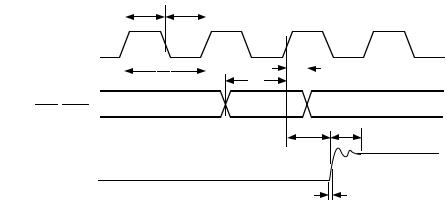
ANALOG OUTPUTS
(IOR, IOG, IOB, ISYNC )
t7
NOTES
1.OUTPUT DELAY (t6) MEASURED FROM THE 50% POINT OF THE RISING EDGE OF CLOCK TO THE 50% POINT OF FULL-SCALE TRANSITION.
2.TRANSITION TIME (t8) MEASURED FROM THE 50% POINT OF FULL-SCALE TRANSITION TO WITHIN 2% OF THE FINAL OUTPUT VALUE.
3.OUTPUT RISE/FALL TIME (t7) MEASURED BETWEEN THE 10% AND 90% POINTS OF FULL TRANSITION.
Figure 1. Video Input/Output Timing
REV. B |
–3– |

ADV7120
RECOMMENDED OPERATING CONDITIONS
Parameter |
Symbol |
Min |
Typ |
Max |
Units |
|
|
|
|
|
|
Power Supply |
VAA |
4.75 |
5.00 |
5.25 |
Volts |
Ambient Operating |
|
0 |
|
+70 |
°C |
Temperature |
TA |
|
|||
Output Load |
RL |
|
37.5 |
|
Ω |
Reference Voltage |
VREF |
1.14 |
1.235 |
1.26 |
Volts |
ABSOLUTE MAXIMUM RATINGS1 |
|
|
|
||
VAA to GND . . . . |
. . . . . . . . . |
. . . . . . |
. . . . . . . |
. . . . . . |
. . +7 V |
Voltage on Any Digital Pin . . . . . GND –0.5 V to VAA +0.5 V |
|
Ambient Operating Temperature (TA) . . . . . |
. . . 0°C to +70°C |
Storage Temperature (TS) . . . . . . . . . . . . . . |
–65°C to +150°C |
Junction Temperature (TJ) . . . . . . . . . . . . . . |
. . . . . . +150°C |
Soldering Temperature (10 secs) . . . . . . . . . . |
. . . . . . . . 300°C |
Vapor Phase Soldering (1 minute) . . . . . . . . . |
. . . . . . . . 220°C |
IOR, IOB, IOG, ISYNC to GND2 . . . . . . . . . . |
. . . . 0 V to VAA |
NOTES
1Stresses above those listed under “Absolute Maximum Ratings” may cause permanent damage to the device. This is a stress rating only and functional operation of the device at these or any other conditions above those listed in the operational sections of this specification is not implied. Exposure to absolute maximum rating conditions for extended periods may affect device reliability.
2Analog Output Short Circuit to any Power Supply or Common can be of an indefinite duration.
ORDERING GUIDE
|
|
Temperature |
Package |
Model |
Speed |
Range1 |
Option2 |
|
|
|
|
ADV7120KN80 |
80 MHz |
0°C to +70°C |
N-40A |
ADV7120KN50 |
50 MHz |
0°C to +70°C |
N-40A |
ADV7120KN30 |
30 MHz |
0°C to +70°C |
N-40A |
ADV7120KP80 |
80 MHz |
0°C to +70°C |
P-44A |
ADV7120KP50 |
50 MHz |
0°C to +70°C |
P-44A |
ADV7120KP30 |
30 MHz |
0°C to +70°C |
P-44A |
ADV7120KST50 |
50 MHz |
0°C to +70°C |
ST-48 |
ADV7120KST30 |
30 MHz |
0°C to +70°C |
ST-48 |
NOTES
1Industrial temperature range (–40°C to +85°C) version available to special request. Please consult your local Analog Device representative.
2N = Plastic DIP; P = Plastic Leaded Chip Carrier.
CAUTION
ESD (electrostatic discharge) sensitive device. Electrostatic charges as high as 4000 V readily accumulate on the human body and test equipment and can discharge without detection. Although the ADV7120 features proprietary ESD protection circuitry, permanent damage may occur on devices subjected to high energy electrostatic discharges. Therefore, proper ESD precautions are recommended to avoid performance degradation or loss of functionality.
PIN CONFIGURATIONS
DIP |
PLCC |
WARNING!
ESD SENSITIVE DEVICE
TQFP
R4 |
|
|
|
|
|
R3 |
|
|
|
1 |
|
|
|
40 |
|
|
|
||
R5 |
|
|
|
|
|
R2 |
|
|
|
2 |
|
|
|
39 |
|
|
|
||
R6 |
|
|
|
|
|
R1 |
|
|
|
3 |
|
|
|
38 |
|
|
|
||
R7 |
|
|
|
|
|
R0 |
|
|
|
4 |
|
|
|
37 |
|
|
|
||
G0 |
|
|
|
|
|
FS ADJUST |
|
|
|
5 |
|
|
|
36 |
G0 |
7 |
|||
G1 |
|
|
|
|
|
VREF |
|
||
6 |
|
|
|
35 |
|
G1 |
8 |
||
G2 |
|
|
|
|
|
|
|||
7 |
|
|
|
34 |
COMP |
|
G2 |
9 |
|
|
|
|
|
|
|
|
|
||
G3 |
8 |
|
|
|
33 |
IOR |
|
G3 |
10 |
|
|
|
|
|
|
|
|
||
G4 |
9 |
ADV7120 |
32 |
IOG |
|
G4 |
11 |
||
|
|
|
|
|
|||||
G5 |
10 |
31 |
ISYNC |
|
|||||
TOP VIEW |
|
G5 |
12 |
||||||
|
|
|
|
|
|||||
G6 |
11 |
(Not to Scale) |
30 |
VAA |
|
G6 |
13 |
||
|
|
|
|
|
|
|
|
||
G7 |
12 |
|
|
|
29 |
IOB |
|
|
|
BLANK |
|
|
|
|
|
|
|
G7 |
14 |
13 |
|
|
|
28 |
GND |
|
|||
|
|
|
|
|
|
||||
|
|
|
|
|
|
|
BLANK |
15 |
|
SYNC |
14 |
|
|
|
27 |
GND |
|||
|
|
|
|
|
|
|
|
SYNC 16 |
|
V |
15 |
|
|
|
26 |
GND |
|
||
AA |
|
|
|
|
|
|
|
|
|
|
|
|
|
|
|
|
|
VAA |
17 |
B0 |
16 |
|
|
|
25 |
CLOCK |
|
||
|
|
|
|
|
|
|
|
|
|
B1 |
17 |
|
|
|
24 |
REF WHITE |
|
|
|
|
|
|
|
|
|
|
|
|
|
B2 |
18 |
|
|
|
23 |
B7 |
|
|
|
|
|
|
|
|
|
|
|
|
|
B3 |
19 |
|
|
|
22 |
B6 |
|
|
|
|
|
|
|
|
|
|
|
|
|
B4 |
20 |
|
|
|
21 |
B5 |
|
|
|
|
|
|
|
|
|
|
|
|
|
R7 |
R6 |
R5 |
R4 |
R3 |
R2 |
R1 |
R0 |
ADJUSTFS |
V |
COMP |
|
|
|
|
GND |
|
R7 |
|
R6 |
R5 |
|
R4 |
|
R3 |
|
R2 |
|
R1 |
|
R0 |
|
GND |
|
GND |
NC |
|
||||
|
|
|
|
|
|
|
|
|
REF |
|
|
|
|
|
|
|
|
|
|
|
|
|
|
|
|
|
|
|
|
|
|
|
|
|
|
|
|
|
|
|
|
|
|
|
|
|
|
|
|
|
|
|
|
|
48 |
|
47 |
|
46 |
|
45 |
|
44 |
|
43 |
|
42 |
|
41 |
|
40 |
|
39 |
|
38 |
|
37 |
|
|
|
|
6 |
5 |
4 |
3 |
2 |
1 |
44 |
43 |
42 |
41 |
40 |
|
GND |
|
|
|
|
|
|
|
|
|
|
|
|
|
|
|
|
|
|
|
|
|
|
|
|
|
|
|
FS ADJUST |
|
|
|
|
|
|
|
|
|
|
|
|
1 |
|
|
|
|
|
|
|
|
|
|
|
|
|
|
|
|
|
|
|
|
|
|
|
|
|
36 |
||
|
|
|
|
|
|
|
|
|
|
39 |
IOR |
G0 |
|
|
|
|
|
|
|
|
|
|
|
|
|
|
|
|
|
|
|
|
|
|
|
|
|
|
|
V |
|
|
|
|
|
|
|
|
|
|
2 |
|
|
|
|
|
|
|
|
|
|
|
|
|
|
|
|
|
|
|
|
|
|
|
|
|
35 |
||||
|
|
|
|
|
|
|
|
|
|
|
|
|
|
|
|
|
|
|
|
|
|
|
|
|
|
|
|
|
|
|
|
|
|
|
|
|
REF |
|||
|
|
|
|
|
|
|
|
|
|
38 |
IOG |
G1 |
|
|
|
|
|
|
|
|
|
|
|
|
|
|
|
|
|
|
|
|
|
|
|
|
|
|
|
COMP |
|
|
|
|
|
|
|
|
|
|
3 |
|
|
|
|
|
|
|
|
|
|
|
|
|
|
|
|
|
|
|
|
|
|
|
|
|
34 |
||||
|
|
|
|
|
|
|
|
|
|
37 |
ISYNC |
G2 |
|
|
|
|
|
|
|
|
|
|
|
|
|
|
|
|
|
|
|
|
|
|
|
|
|
|
|
IOR |
|
|
|
|
|
|
|
|
|
|
4 |
|
|
|
|
|
|
|
|
|
|
|
|
|
|
|
|
|
|
|
|
|
|
|
|
|
33 |
||||
|
|
|
|
|
|
|
|
|
|
36 |
VAA |
G3 |
|
|
|
|
|
|
|
|
|
|
|
|
|
|
|
|
|
|
|
|
|
|
|
|
|
|
|
IOG |
|
|
|
|
|
|
|
|
|
|
5 |
|
|
|
|
|
|
|
|
|
|
ADV7120 |
|
|
|
|
|
|
|
|
|
|
|
32 |
|||||||
|
|
|
|
|
|
|
|
|
|
35 |
|
G4 |
|
|
|
|
|
|
|
|
|
|
|
|
|
|
|
|
|
|
|
|
|
|
|
VAA |
||||
|
|
|
|
ADV7120 |
|
|
|
VAA |
6 |
|
|
|
|
|
|
|
|
|
|
TOP VIEW |
|
|
|
|
|
|
|
|
|
|
31 |
|||||||||
|
|
|
|
TOP VIEW |
|
|
|
|
|
G5 |
|
|
|
|
|
|
|
|
|
|
|
|
|
|
|
|
|
|
|
|
|
|
VAA |
|||||||
|
|
|
|
|
|
|
34 |
VAA |
7 |
|
|
|
|
|
|
|
|
|
(Not to Scale) |
|
|
|
|
|
|
|
|
|
30 |
|||||||||||
|
|
|
|
(Not to Scale) |
|
|
|
|
|
G6 |
|
|
|
|
|
|
|
|
|
|
|
|
|
|
|
|
|
|
|
|
|
|
|
|
|
|
|
IOB |
||
|
|
|
|
|
|
|
|
|
|
33 |
IOB |
8 |
|
|
|
|
|
|
|
|
|
|
|
|
|
|
|
|
|
|
|
|
|
|
|
|
|
29 |
||
|
|
|
|
|
|
|
|
|
|
|
|
G7 |
|
|
|
|
|
|
|
|
|
|
|
|
|
|
|
|
|
|
|
|
|
|
|
|
|
|
|
GND |
|
|
|
|
|
|
|
|
|
|
32 |
GND |
9 |
|
|
|
|
|
|
|
|
|
|
|
|
|
|
|
|
|
|
|
|
|
|
|
|
|
28 |
||
|
|
|
|
|
|
|
|
|
|
|
|
|
|
|
|
|
|
|
|
|
|
|
|
|
|
|
|
|
|
|
|
|
|
|
|
|
|
|
|
GND |
|
|
|
|
|
|
|
|
|
|
31 |
GND |
BLANK |
10 |
|
|
|
|
|
|
|
|
|
|
|
|
|
|
|
|
|
|
|
|
|
|
|
|
|
27 |
|
|
|
|
|
|
|
|
|
|
|
|
|
|
|
|
|
|
|
|
|
|
|
|
|
|
|
|
|
|
|
|
|
|
|
|
|
|
|
|
|
CLOCK |
|
|
|
|
|
|
|
|
|
|
30 |
GND |
SYNC |
11 |
|
|
|
|
|
|
|
|
|
|
|
|
|
|
|
|
|
|
|
|
|
|
|
|
|
26 |
|
|
|
|
|
|
|
|
|
|
|
|
|
VAA |
|
|
|
|
|
|
|
|
|
|
|
|
|
|
|
|
|
|
|
|
|
|
|
|
|
|
|
NC |
|
|
|
|
|
|
|
|
|
|
29 |
GND |
12 |
|
|
|
|
|
|
|
|
|
|
|
|
|
|
|
|
|
|
|
|
|
|
|
|
|
25 |
||
|
|
|
|
|
|
|
|
|
|
|
|
|
|
|
|
|
|
|
|
|
|
|
|
|
|
|
|
|
|
|
|
|
|
|
|
|
|
|
|
|
18 |
19 |
20 |
21 |
22 |
23 |
24 |
25 |
26 |
27 |
28 |
|
|
|
13 |
|
14 |
|
15 |
|
16 |
|
17 |
|
18 |
|
19 |
|
20 |
|
21 |
|
22 |
|
23 |
|
24 |
|
|
|
|
|
|
|
|
NC |
|
GND |
|
GND |
B0 |
|
B1 |
|
B2 |
|
B3 |
|
B4 |
|
B5 |
|
B6 |
|
B7 |
NC |
|
|||||||||||||||
B0 |
B1 |
B2 |
B3 |
B4 |
B5 |
B6 |
B7 |
WHITEREF |
CLOCK |
GND |
|
|
|
|
|
|
|
|
|
|
|
|
|
|
||||||||||||||||
NC = NO CONNECT
NOTE
For the ADV7120 in TQFP package: The REF WHITE pin is not available. The ISYNC pin is not available and is internally connected to the IOG pin.
–4– |
REV. B |
Loading...