


 Loading...
ANALOG DEVICES ADSP-21060, ADSP-21060L, ADSP-21062, ADSP-21062L, ADSP-21060C Service Manual
...
SHARC Processor
ADSP-21060/ADSP-21060L/ADSP-21062/ADSP-21062L/ADSP-21060C/ADSP-21060LC
SUMMARY
High performance signal processor for communications, graphics and imaging applications
Super Harvard Architecture
4 independent buses for dual data fetch, instruction fetch, and nonintrusive I/O
32-bit IEEE floating-point computation units—multiplier, ALU, and shifter
Dual-ported on-chip SRAM and integrated I/O peripherals—a complete system-on-a-chip
Integrated multiprocessing features
240-lead thermally enhanced MQFP_PQ4 package, 225-ball plastic ball grid array (PBGA), 240-lead hermetic CQFP package
RoHS compliant packages
KEY FEATURES—PROCESSOR CORE
40 MIPS, 25 ns instruction rate, single-cycle instruction execution
120 MFLOPS peak, 80 MFLOPS sustained performance Dual data address generators with modulo and bit-reverse
addressing)
Efficient program sequencing with zero-overhead looping: Single-cycle loop setup
IEEE JTAG Standard 1149.1 Test Access Port and on-chip emulation
32-bit single-precision and 40-bit extended-precision IEEE floating-point data formats or 32-bit fixed-point data format
CORE PROCESSOR |
DUAL-PORTED SRAM |
|
|
TIMER |
INSTRUCTION |
|
TWO INDEPENDENT |
|
0 |
|
|||
|
|
|
|
CACHE |
|
|
LOCKB |
BLOCK1 |
|||
|
|
|
|
|
DUAL-PORTED BLOCKS |
|
|||||
|
|
|
|
32 48-BIT |
|
||||||
|
|
|
|
ADDR |
DATA |
DATA |
ADDR |
||||
|
|
|
|
|
|
||||||
|
|
|
|
|
|
PROCESSOR PORT |
I/O PORT |
|
|
||
DAG1 |
DAG2 |
|
|
|
|
ADDR |
DATA |
|
|
|
|
PROGRAM |
|
|
|
|
|
|
|||||
8 4 32 |
8 4 24 |
|
|
|
|
|
|
||||
SEQUENCER |
|
|
|
|
|
|
|||||
|
|
|
|
|
|
|
|
||||
|
|
|
|
|
24 |
|
|
|
IOD |
IOA |
|
|
PM ADDRESS BUS |
|
|
|
|
48 |
17 |
|
|||
|
DM ADDRESS BUS |
|
|
32 |
|
|
|
|
|
|
|
|
|
PM DATA BUS |
|
|
48 |
|
|
|
|
|
|
BUS |
|
|
|
|
|
|
|
|
|
|
|
CONNECT |
DM DATA BUS |
40/32 |
|
|
|
|
|
|
|||
(PX) |
|
|
|
|
|
|
|
||||
|
|
|
|
|
|
|
|
||||
|
|
|
|
|
|
|
|
|
|
|
|
S
JTAG 7
TEST AND
EMULATION
EXTERNAL
PORT
32
ADDR BUS
MUX
MULTIPROCESSOR
INTERFACE
48
DATA BUS
MUX
HOST PORT
|
DATA |
IOP |
DMA |
4 |
|
REGISTER |
CONTROLLER |
|
|
|
REGISTERS |
|
||
|
FILE |
|
6 |
|
|
(MEMORY |
|
||
|
|
SERIAL PORTS |
|
|
MULT |
16 40-BIT BARREL |
MAPPED) |
6 |
|
ALU |
(2) |
|||
|
SHIFTER |
CONTROL, |
|
|
|
|
STATUS AND |
LINK PORTS |
36 |
|
|
DATA BUFFERS |
|
|
|
|
(6) |
|
|
|
|
|
|
|
|
|
I/O PROCESSOR |
|
|
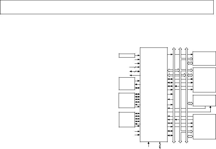
Figure 1. Functional Block Diagram
SHARC and the SHARC logo are registered trademarks of Analog Devices, Inc.
Rev. G
Information furnished by Analog Devices is believed to be accurate and reliable. However, no responsibility is assumed by Analog Devices for its use, nor for any infringements of patents or other rights of third parties that may result from its use. Specifications subject to change without notice. No license is granted by implication or otherwise under any patent or patent rights of Analog Devices. Trademarks and registered trademarks are the property of their respective owners.
One Technology Way, P.O. Box 9106, Norwood, MA 02062-9106 U.S.A. Tel : 781.329.4700 www.analog.com Fax: 781.461.3113 ©2010 Analog Devices, Inc. All rights reserved.

ADSP-21060/ADSP-21060L/ADSP-21062/ADSP-21062L/ADSP-21060C/ADSP-21060LC
PARALLEL COMPUTATIONS
Single-cycle multiply and ALU operations in parallel with dual memory read/writes and instruction fetch
Multiply with add and subtract for accelerated FFT butterfly computation
UP TO 4M BIT ON-CHIP SRAM
Dual-ported for independent access by core processor and DMA
OFF-CHIP MEMORY INTERFACING
4 gigawords addressable
Programmable wait state generation, page-mode DRAM support
DMA CONTROLLER
10 DMA channels for transfers between ADSP-2106x internal memory and external memory, external peripherals, host processor, serial ports, or link ports
Background DMA transfers at up to 40 MHz, in parallel with full-speed processor execution
Table 1. ADSP-2106x SHARC Processor Family Features
HOST PROCESSOR INTERFACE TO 16AND 32-BIT MICROPROCESSORS
Host can directly read/write ADSP-2106x internal memory and IOP registers
MULTIPROCESSING
Glueless connection for scalable DSP multiprocessing architecture
Distributed on-chip bus arbitration for parallel bus connect of up to six ADSP-2106xs plus host
Six link ports for point-to-point connectivity and array multiprocessing
240 MBps transfer rate over parallel bus
240 MBps transfer rate over link ports
SERIAL PORTS
Two 40 Mbps synchronous serial ports with companding hardware
Independent transmit and receive functions
Feature |
ADSP-21060 |
ADSP-21062 |
ADSP-21060L |
ADSP-21062L |
ADSP-21060C |
ADSP-21060LC |
|
|
|
|
|
|
|
SRAM |
4M bits |
2M bits |
4M bits |
2M bits |
4M bits |
4M bits |
|
|
|
|
|
|
|
Operating |
|
|
|
|
|
|
Voltage |
5 V |
5 V |
3.3 V |
3.3 V |
5 V |
3.3 V |
|
|
|
|
|
|
|
Instruction |
33 MHz |
33 MHz |
33 MHz |
33 MHz |
33 MHz |
33 MHz |
Rate |
40 MHz |
40 MHz |
40 MHz |
40 MHz |
40 MHz |
40 MHz |
|
|
|
|
|
|
|
|
MQFP_PQ4 |
MQFP_PQ4 |
MQFP_PQ4 |
MQFP_PQ4 |
|
|
Package |
PBGA |
PBGA |
PBGA |
PBGA |
CQFP |
CQFP |
|
|
|
|
|
|
|
Rev. G | Page 2 of 64 | August 2010

ADSP-21060/ADSP-21060L/ADSP-21062/ADSP-21062L/ADSP-21060C/ADSP-21060LC
CONTENTS |
|
Summary ............................................................... |
1 |
Revision History ...................................................... |
3 |
General Description ................................................. |
4 |
SHARC Family Core Architecture ............................ |
4 |
Memory and I/O Interface Features ........................... |
5 |
Development Tools ............................................... |
8 |
Evaluation Kit ...................................................... |
9 |
Designing an Emulator-Compatible DSP Board |
|
(Target) ........................................................... |
9 |
Additional Information .......................................... |
9 |
Related Signal Chains ............................................ |
9 |
Pin Function Descriptions ........................................ |
10 |
Target Board Connector for EZ-ICE Probe ................ |
13 |
ADSP-21060/ADSP-21062 Specifications ..................... |
15 |
Operating Conditions (5 V) .................................... |
15 |
Electrical Characteristics (5 V) ................................ |
15 |
Internal Power Dissipation (5 V) ............................. |
16 |
REVISION HISTORY |
|
8/10—Rev. F to Rev. G |
|
Added new section, Related Signal Chains ....................... |
9 |
Revised Table 14 ..................................................... |
25 |
Revised Table 15 ..................................................... |
26 |
Revised Table 28 ..................................................... |
43 |
Clarification of Table 41 Title ..................................... |
54 |
Clarification of Table 42 Title ..................................... |
55 |
Changes to Ordering Guide ....................................... |
62 |
External Power Dissipation (5 V) ............................ |
17 |
ADSP-21060L/ADSP-21062L Specifications ................. |
18 |
Operating Conditions (3.3 V) ................................. |
18 |
Electrical Characteristics (3.3 V) ............................. |
18 |
Internal Power Dissipation (3.3 V) .......................... |
19 |
External Power Dissipation (3.3 V) .......................... |
20 |
Absolute Maximum Ratings ................................... |
20 |
ESD Caution ...................................................... |
21 |
Package Marking Information ................................ |
21 |
Timing Specifications ........................................... |
21 |
Test Conditions .................................................. |
48 |
Environmental Conditions .................................... |
51 |
225-Ball PBGA Ball Configuration .............................. |
52 |
240-Lead MQFP_PQ4/CQFP Pin Configuration ............ |
54 |
Outline Dimensions ................................................ |
56 |
Surface-Mount Design .......................................... |
61 |
Ordering Guide ..................................................... |
62 |
Rev. G | Page 3 of 64 | August 2010
ADSP-21060/ADSP-21060L/ADSP-21062/ADSP-21062L/ADSP-21060C/ADSP-21060LC
GENERAL DESCRIPTION
The ADSP-2106x SHARC®—Super Harvard Architecture Com- puter—is a 32-bit signal processing microcomputer that offers high levels of DSP performance. The ADSP-2106x builds on the ADSP-21000 DSP core to form a complete system-on-a-chip, adding a dual-ported on-chip SRAM and integrated I/O peripherals supported by a dedicated I/O bus.
Fabricated in a high speed, low power CMOS process, the ADSP-2106x has a 25 ns instruction cycle time and operates at 40 MIPS. With its on-chip instruction cache, the processor can execute every instruction in a single cycle. Table 2 shows performance benchmarks for the ADSP-2106x.
The ADSP-2106x SHARC represents a new standard of integration for signal computers, combining a high performance floating-point DSP core with integrated, on-chip system features including up to 4M bit SRAM memory (see Table 1), a host processor interface, DMA controller, serial ports and link port, and parallel bus connectivity for glueless DSP multiprocessing.
Table 2. Benchmarks (at 40 MHz)
Benchmark Algorithm |
Speed |
Cycles |
1024 Point Complex FFT (Radix 4, with |
0.46 μs |
18,221 |
reversal) |
|
|
FIR Filter (per tap) |
25 ns |
1 |
IIR Filter (per biquad) |
100 ns |
4 |
Divide (y/x) |
150 ns |
6 |
Inverse Square Root |
225 ns |
9 |
DMA Transfer Rate |
240 Mbytes/s |
|
The ADSP-2106x continues SHARC’s industry-leading standards of integration for DSPs, combining a high performance 32-bit DSP core with integrated, on-chip system features.
The block diagram on Page 1 illustrates the following architectural features:
•Computation units (ALU, multiplier and shifter) with a shared data register file
•Data address generators (DAG1, DAG2)
•Program sequencer with instruction cache
•PM and DM buses capable of supporting four 32-bit data transfers between memory and the core at every core processor cycle
•Interval timer
•On-chip SRAM
•External port for interfacing to off-chip memory and peripherals
•Host port and multiprocessor Interface
•DMA controller
•Serial ports and link ports
•JTAG Test Access Port
|
|
ADSP-2106x |
|
|
|
|
|
|
1 3 CLOCK |
|
CLKIN |
BMS |
|
|
|
CS |
BOOT |
|
|
|
|
|
|
|||
|
|
EBOOT |
|
|
|
|
ADDR |
EPROM |
|
|
|
|
|
|
|
(OPTIONAL) |
|
|
|
LBOOT |
|
|
|
|
DATA |
|
|
3 |
|
|
|
|
|
||
|
IRQ2–0 |
|
|
|
|
|
|
|
|
4 |
|
|
|
|
|
|
|
|
FLAG3–0 |
ADDR31–0 |
|
|
|
ADDR |
|
|
|
|
|
|
|
|
|
|
|
|
|
TIMEXP |
DATA47–0 |
|
|
|
DATA |
MEMORY- |
LINK |
|
|
RD |
|
|
|
OE |
MAPPED |
|
LxCLK |
|
|
|
DEVICES |
|||
DEVICES |
|
WR |
|
|
|
WE |
||
|
LxACK |
|
|
|
(OPTIONAL) |
|||
(6 MAX) |
|
ACK |
|
|
|
ACK |
|
|
(OPTIONAL) |
|
LxDAT3–0 |
|
|
|
|
||
|
MS3–0 |
|
|
|
CS |
|
||
|
|
|
|
|
|
|
||
|
|
TCLK0 |
PAGE |
CONTROL |
ADDRESS |
DATA |
|
|
SERIAL |
|
RCLK0 |
|
DMA DEVICE |
||||
DEVICE |
|
TFS0 |
SBTS |
(OPTIONAL) |
||||
(OPTIONAL) |
|
RSF0 |
|
DATA |
|
|||
|
|
DT0 |
ADRCLK |
|
|
|
|
|
|
|
|
|
|
|
|
||
|
|
DR0 |
DMAR1–2 |
|
|
|
|
|
|
|
|
|
|
|
|
|
|
|
|
TCLK1 |
DMAG1–2 |
|
|
|
|
|
|
|
|
|
|
|
|
|
|
SERIAL |
|
RCLK1 |
CS |
|
|
|
|
HOST |
DEVICE |
|
TFS1 |
HBR |
|
|
|
|
|
|
RSF1 |
|
|
|
PROCESSOR |
|||
(OPTIONAL) |
|
HBG |
|
|
|
|||
|
DT1 |
|
|
|
INTERFACE |
|||
|
|
|
|
|
||||
|
|
DR1 |
REDY |
|
|
|
(OPTIONAL) |
|
|
|
RPBA |
BR1–6 |
|
|
|
ADDR |
|
|
|
ID2–0 |
PA |
|
|
|
DATA |
|
|
|
RESET |
JTAG |
|
|
|
|
|
|
|
|
6 |
|
|
|
|
|
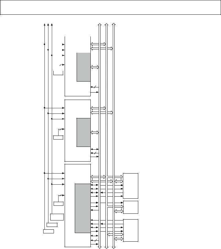
Figure 2. ADSP-2106x System Sample Configuration
SHARC FAMILY CORE ARCHITECTURE
The ADSP-2106x includes the following architectural features of the ADSP-21000 family core. The ADSP-2106x processors are codeand function-compatible with the ADSP-21020.
Independent, Parallel Computation Units
The arithmetic/logic unit (ALU), multiplier and shifter all perform single-cycle instructions. The three units are arranged in parallel, maximizing computational throughput. Single multifunction instructions execute parallel ALU and multiplier operations. These computation units support IEEE 32-bit singleprecision floating-point, extended precision 40-bit floatingpoint, and 32-bit fixed-point data formats.
Data Register File
A general–purpose data register file is used for transferring data between the computation units and the data buses, and for storing intermediate results. This 10-port, 32-register (16 primary, 16 secondary) register file, combined with the ADSP-21000 Harvard architecture, allows unconstrained data flow between computation units and internal memory.
Rev. G | Page 4 of 64 | August 2010

ADSP-21060/ADSP-21060L/ADSP-21062/ADSP-21062L/ADSP-21060C/ADSP-21060LC
Single-Cycle Fetch of Instruction and Two Operands
The ADSP-2106x features an enhanced Harvard architecture in which the data memory (DM) bus transfers data and the program memory (PM) bus transfers both instructions and data (see Figure 1 on Page 1). With its separate program and data memory buses and on-chip instruction cache, the processor can simultaneously fetch two operands and an instruction (from the cache), all in a single cycle.
Instruction Cache
The ADSP-2106x includes an on-chip instruction cache that enables three-bus operation for fetching an instruction and two data values. The cache is selective—only the instructions whose fetches conflict with PM bus data accesses are cached. This allows full-speed execution of core, looped operations such as digital filter multiply-accumulates and FFT butterfly processing.
Data Address Generators with Hardware Circular Buffers
The ADSP-2106x’s two data address generators (DAGs) implement circular data buffers in hardware. Circular buffers allow efficient programming of delay lines and other data structures required in digital signal processing, and are commonly used in digital filters and Fourier transforms. The two DAGs of the ADSP-2106x contain sufficient registers to allow the creation of up to 32 circular buffers (16 primary register sets, 16 secondary). The DAGs automatically handle address pointer wraparound, reducing overhead, increasing performance and simplifying implementation. Circular buffers can start and end at any memory location.
Flexible Instruction Set
The 48-bit instruction word accommodates a variety of parallel operations, for concise programming. For example, the ADSP-2106x can conditionally execute a multiply, an add, a subtract and a branch, all in a single instruction.
MEMORY AND I/O INTERFACE FEATURES
The ADSP-2106x processors add the following architectural features to the SHARC family core.
Dual-Ported On-Chip Memory
The ADSP-21062/ADSP-21062L contains two megabits of onchip SRAM, and the ADSP-21060/ADSP-21060L contains
4M bits of on-chip SRAM. The internal memory is organized as two equal sized blocks of 1M bit each for the ADSP-21062/ ADSP-21062L and two equal sized blocks of 2M bits each for the ADSP-21060/ADSP-21060L. Each can be configured for different combinations of code and data storage. Each memory block is dual-ported for single-cycle, independent accesses by the core processor and I/O processor or DMA controller. The dual-ported memory and separate on-chip buses allow two data transfers from the core and one from I/O, all in a single cycle.
On the ADSP-21062/ADSP-21062L, the memory can be configured as a maximum of 64k words of 32-bit data, 128k words of 16-bit data, 40k words of 48-bit instructions (or 40-bit data), or combinations of different word sizes up to two megabits. All of the memory can be accessed as 16-bit, 32-bit, or 48-bit words.
On the ADSP-21060/ADSP-21060L, the memory can be configured as a maximum of 128k words of 32-bit data, 256k words of 16-bit data, 80k words of 48-bit instructions (or 40-bit data), or combinations of different word sizes up to four megabits. All of the memory can be accessed as 16-bit, 32-bit or 48-bit words.
A 16-bit floating-point storage format is supported, which effectively doubles the amount of data that can be stored on-chip. Conversion between the 32-bit floating-point and 16-bit float- ing-point formats is done in a single instruction.
While each memory block can store combinations of code and data, accesses are most efficient when one block stores data, using the DM bus for transfers, and the other block stores instructions and data, using the PM bus for transfers. Using the DM bus and PM bus in this way, with one dedicated to each memory block, assures single-cycle execution with two data transfers. In this case, the instruction must be available in the cache. Single-cycle execution is also maintained when one of the data operands is transferred to or from off-chip, via the ADSP-2106x’s external port.
On-Chip Memory and Peripherals Interface
The ADSP-2106x’s external port provides the processor’s interface to off-chip memory and peripherals. The 4-gigaword offchip address space is included in the ADSP-2106x’s unified address space. The separate on-chip buses—for PM addresses, PM data, DM addresses, DM data, I/O addresses, and I/O data—are multiplexed at the external port to create an external system bus with a single 32-bit address bus and a single 48-bit (or 32-bit) data bus.
Addressing of external memory devices is facilitated by on-chip decoding of high-order address lines to generate memory bank select signals. Separate control lines are also generated for simplified addressing of page-mode DRAM. The ADSP-2106x provides programmable memory wait states and external memory acknowledge controls to allow interfacing to DRAM and peripherals with variable access, hold and disable time requirements.
Host Processor Interface
The ADSP-2106x’s host interface allows easy connection to standard microprocessor buses, both 16-bit and 32-bit, with little additional hardware required. Asynchronous transfers at speeds up to the full clock rate of the processor are supported. The host interface is accessed through the ADSP-2106x’s external port and is memory-mapped into the unified address space. Four channels of DMA are available for the host interface; code and data transfers are accomplished with low software overhead.
The host processor requests the ADSP-2106x’s external bus with the host bus request (HBR), host bus grant (HBG), and ready (REDY) signals. The host can directly read and write the internal memory of the ADSP-2106x, and can access the DMA channel setup and mailbox registers. Vector interrupt support is provided for efficient execution of host commands.
Rev. G | Page 5 of 64 | August 2010
ADSP-21060/ADSP-21060L/ADSP-21062/ADSP-21062L/ADSP-21060C/ADSP-21060LC
|
|
|
|
|
|
|
ADSP-2106x #6 |
|
|
|
|
|
|
|
|
|
|
|
ADSP-2106x #5 |
|
|
|
|
|
|
|
|
|
|
|
ADSP-2106x #4 |
CONTROL |
ADDRESS |
DATA |
|
|
|
|
|
|
|
|
|
||||
|
|
|
|
|
|
|
|
|
|||
|
|
|
|
|
|
|
ADSP-2106x #3 |
||||
|
|
|
|
|
|
|
CLKIN |
ADDR31–0 |
|
|
|
|
|
|
|
|
|
|
|
|
|
||
|
|
|
|
|
|
|
|
|
|
|
|
|
|
|
|
|
|
|
RESET |
DATA47–0 |
|
|
|
|
|
|
|
|
|
|
|
|
|
|
|
|
|
|
|
|
|
|
RPBA |
|
|
|
|
|
|
|
|
|
|
|
|
|
|
|
|
|
|
3 |
|
|
|
|
|||||
|
|
|
|
ID2–0 |
|
|
|
|
|||
|
|
|
|
|
|
|
CONTROL |
|
|
|
|
|
|
|
|
|
|
|
|
|
|
||
|
|
|
|
|
|
|
|
|
|
|
|
|
|
|
|
|
|
|
|
|
|
|
|
011
BR1–2, BR4–6 |
5 |
|
|
||
|
|
|
|||
|
|
BR3 |
|
|
|
ADSP-2106x #2 |
|
|
|
||
CLKIN |
ADDR31–0 |
|
|
|
|
RESET |
DATA47–0 |
|
|
|
|
|
|
|
|
|
|
RPBA |
|
|
|
|
|
3 |
|
|
|
|
|
ID2–0 |
|
|
|
|
|
|
CONTROL |
|
|
|
|
010 |
|
|
|
|
|
|
|
CPA |
5 |
|
|
|
BR1, BR3–6 |
|
|
||
|
|
|
|
||
|
|
BR2 |
CONTROL |
ADDRESS |
|
ADSP-2106x #1 |
DATA |
||||
CLKIN |
|
|
|
|
|
RESET |
ADDR31–0 |
|
|
ADDR |
|
DATA47–0 |
|
|
DATA |
||
|
|
|
|||
RPBA |
|
RDx |
|
|
OE |
|
|
|
|
||
|
|
WRx |
|
|
WE |
3 |
CONTROL |
ACK |
|
|
ACK |
ID2–0 |
MS3–0 |
|
|
CS |
|
|
|
|
|||
|
|
|
|
|
|
001 |
|
BMS |
|
|
CS |
|
|
PAGE |
|
|
ADDR |
|
|
SBTS |
|
|
DATA |
|
|
|
|
|
|
BUS |
|
|
|
|
|
PRIORITY |
|
CS |
|
|
|
|
|
|
|
|
|
RESET |
|
HBR |
|
|
|
|
HBG |
|
|
|
|
|
|
|
|
|
|
CLOCK |
|
REDY |
|
|
|
|
|
CPA |
|
|
ADDR |
|
|
5 |
|
DATA |
|
|
|
BR2–6 |
|
||
|
|
|
|
||
|
|
|
|
|
|
|
|
BR1 |
|
|
|
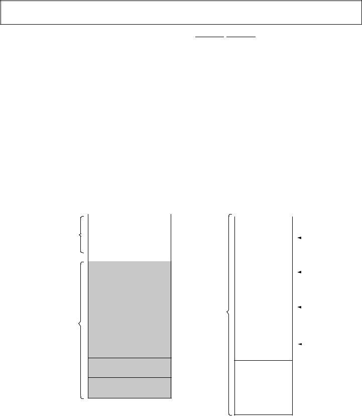
GLOBAL MEMORY AND
PERIPHERAL (OPTIONAL)
BOOT EPROM (OPTIONAL)
HOST PROCESSOR INTERFACE (OPTIONAL)
Figure 3. Shared Memory Multiprocessing System
Rev. G | Page 6 of 64 | August 2010
ADSP-21060/ADSP-21060L/ADSP-21062/ADSP-21062L/ADSP-21060C/ADSP-21060LC
DMA Controller
The ADSP-2106x’s on-chip DMA controller allows zero-over- head data transfers without processor intervention. The DMA controller operates independently and invisibly to the processor core, allowing DMA operations to occur while the core is simultaneously executing its program instructions.
DMA transfers can occur between the ADSP-2106x’s internal memory and external memory, external peripherals, or a host processor. DMA transfers can also occur between the ADSP2106x’s internal memory and its serial ports or link ports. DMA transfers between external memory and external peripheral devices are another option. External bus packing to 16-,
32-, or 48-bit words is performed during DMA transfers.
Ten channels of DMA are available on the ADSP-2106x—two via the link ports, four via the serial ports, and four via the processor’s external port (for either host processor, other ADSP-2106xs, memory, or I/O transfers). Four additional link port DMA channels are shared with Serial Port 1 and the external port. Programs can be downloaded to the ADSP-2106x using DMA transfers. Asynchronous off-chip peripherals can
control two DMA channels using DMA request/grant lines
(DMAR1–2, DMAG1–2). Other DMA features include interrupt generation upon completion of DMA transfers and DMA chaining for automatic linked DMA transfers.
Multiprocessing
The ADSP-2106x offers powerful features tailored to multiprocessor DSP systems. The unified address space (see Figure 4) allows direct interprocessor accesses of each ADSP-2106x’s internal memory. Distributed bus arbitration logic is included on-chip for simple, glueless connection of systems containing up to six ADSP-2106xs and a host processor. Master processor changeover incurs only one cycle of overhead. Bus arbitration is selectable as either fixed or rotating priority. Bus lock allows indivisible read-modify-write sequences for semaphores. A vector interrupt is provided for interprocessor commands. Maximum throughput for interprocessor data transfer is
240M bytes/s over the link ports or external port. Broadcast writes allow simultaneous transmission of data to all ADSP-2106xs and can be used to implement reflective semaphores.
|
|
ADDRESS |
|
|
ADDRESS |
|||
|
|
0x0000 0000 |
|
|
0x0040 0000 |
|||
|
IOP REGISTERS |
|
|
|||||
|
|
|
||||||
|
|
|
|
|
||||
|
|
|
|
|
|
|
|
|
INTERNAL |
|
0x0002 0000 |
|
|
|
|
|
|
NORMAL WORD ADDRESSING |
BANK 0 |
|
|
|
||||
|
|
|
|
|
||||
MEMORY |
|
|
|
|
|
|||
(32-BIT DATA WORDS |
|
|
|
|
MS0 |
|||
SPACE |
48-BIT INSTRUCTION WORDS) |
0x0004 0000 |
SDRAM |
|
|
|||
|
|
|
||||||
|
|
|
|
|
|
|
||
|
SHORT WORD ADDRESSING |
|
|
(OPTIONAL) |
|
|
|
|
|
|
|
|
|
|
|
|
|
|
(16-BIT DATA WORDS) |
|
|
|
|
|
|
|
|
|
0x0008 0000 |
|
|
|
|
|
|
|
INTERNAL MEMORY SPACE |
BANK 1 |
|
|
MS1 |
|||
|
|
|
|
|
||||
|
WITH ID = 001 |
|
|
|
|
|
|
|
|
|
0x0010 0000 |
|
|
|
|
|
|
|
INTERNAL MEMORY SPACE |
|
|
|
|
|
||
|
|
|
|
|
|
|
|
|
|
|
|
|
|
|
|
|
|
|
WITH ID = 010 |
|
|
|
|
|
|
|
|
|
0x0018 0000 |
|
|
|
|
MS2 |
|
|
|
|
|
|
|
|||
MULTIPROCESSOR |
INTERNAL MEMORY SPACE |
EXTERNAL |
BANK 2 |
|
|
|||
|
|
|||||||
WITH ID = 011 |
MEMORY |
|
|
|
|
|
||
MEMORY |
|
SPACE |
|
|
|
|
|
|
SPACE |
INTERNAL MEMORY SPACE |
0x0012 0000 |
|
|
|
|
|
|
|
|
|
|
|
|
|
|
|
|
|
|
|
|
|
|
|
|
|
WITH ID = 100 |
|
|
|
|
|
|
|
|
|
0x0028 0000 |
BANK 3 |
|
|
MS3 |
||
|
INTERNAL MEMORY SPACE |
|
|
|||||
|
|
|
|
|
||||
|
|
|
|
|
||||
|
|
|
|
|
|
|
|
|
|
WITH ID = 101 |
|
|
|
|
|
|
|
0x0030 0000
INTERNAL MEMORY SPACE
WITH ID = 110
0x0038 0000
BROADCAST WRITE
NONBANKED
TO ALL ADSP-21061s
0x003F FFFF
0x0FFF FFFF
NOTE: BANK SIZES ARE SELECTED BY
MSIZE BITS IN THE SYSCON REGISTER
Figure 4. Memory Map
Rev. G | Page 7 of 64 | August 2010

ADSP-21060/ADSP-21060L/ADSP-21062/ADSP-21062L/ADSP-21060C/ADSP-21060LC
Link Ports
The ADSP-2106x features six 4-bit link ports that provide additional I/O capabilities. The link ports can be clocked twice per cycle, allowing each to transfer eight bits of data per cycle. Linkport I/O is especially useful for point-to-point interprocessor communication in multiprocessing systems.
The link ports can operate independently and simultaneously, with a maximum data throughput of 240M bytes/s. Link port data is packed into 32or 48-bit words, and can be directly read by the core processor or DMA-transferred to on-chip memory.
Each link port has its own double-buffered input and output registers. Clock/acknowledge handshaking controls link port transfers. Transfers are programmable as either transmit or receive.
Program Booting
The internal memory of the ADSP-2106x can be booted at system power-up from an 8-bit EPROM, a host processor, or through one of the link ports. Selection of the boot source is controlled by the BMS (boot memory select), EBOOT (EPROM Boot), and LBOOT (link/host boot) pins. 32-bit and 16-bit host processors can be used for booting. The processor also supports a no-boot mode in which instruction execution is sourced from the external memory.
DEVELOPMENT TOOLS
The ADSP-2106x is supported by a complete set of CROSSCORE®† software development tools, including Analog Devices emulators and VisualDSP++®‡ development environment. The same emulator hardware that supports other SHARC processors also fully emulates the ADSP-2106x.
The VisualDSP++ project management environment lets programmers develop and debug an application. This environment includes an easy to use assembler (which is based on an algebraic syntax), an archiver (librarian/library builder), a linker, a loader, a cycle-accurate instruction-level simulator, a C/C++ compiler, and a C/C++ runtime library that includes DSP and mathematical functions. A key point for these tools is C/C++ code efficiency. The compiler has been developed for efficient translation of C/C++ code to DSP assembly. The ADSP-2106x SHARC DSP has architectural features that improve the efficiency of compiled C/C++ code.
The VisualDSP++ debugger has a number of important features. Data visualization is enhanced by a plotting package that offers a significant level of flexibility. This graphical representation of user data enables the programmer to quickly determine the performance of an algorithm. As algorithms grow in complexity, this capability can have increasing significance on the designer’s development schedule, increasing productivity. Statistical profiling enables the programmer to nonintrusively poll the processor as it is running the program. This feature, unique to VisualDSP++, enables the software developer to passively gather important code execution metrics without interrupting
† CROSSCORE is a registered trademark of Analog Devices, Inc.
‡ VisualDSP++ is a registered trademark of Analog Devices, Inc.
the real-time characteristics of the program. Essentially, the developer can identify bottlenecks in software quickly and efficiently. By using the profiler, the programmer can focus on those areas in the program that impact performance and take corrective action.
Debugging both C/C++ and assembly programs with the VisualDSP++ debugger, programmers can:
•View mixed C/C++ and assembly code (interleaved source and object information)
•Insert breakpoints
•Set conditional breakpoints on registers, memory, and stacks
•Trace instruction execution
•Perform linear or statistical profiling of program execution
•Fill, dump, and graphically plot the contents of memory
•Perform source level debugging
•Create custom debugger windows
The VisualDSP++ IDDE lets programmers define and manage DSP software development. Its dialog boxes and property pages let programmers configure and manage all of the ADSP-2106x development tools, including the color syntax highlighting in the VisualDSP++ editor. This capability permits:
•Control in how the development tools process inputs and generate outputs
•Maintenance of a one-to-one correspondence with the tools’ command line switches
The VisualDSP++ kernel (VDK) incorporates scheduling and resource management tailored specifically to address the memory and timing constraints of DSP programming. These capabilities enable engineers to develop code more effectively, eliminating the need to start from the very beginning when developing new application code. The VDK features include threads, critical and unscheduled regions, semaphores, events, and device flags. The VDK also supports priority-based, preemptive, cooperative, and time-sliced scheduling approaches. In addition, the VDK was designed to be scalable. If the application does not use a specific feature, the support code for that feature is excluded from the target system.
Because the VDK is a library, a developer can decide whether to use it or not. The VDK is integrated into the VisualDSP++ development environment, but can also be used via standard command line tools. When the VDK is used, the development environment assists the developer with many error-prone tasks and assists in managing system resources, automating the generation of various VDK-based objects, and visualizing the system state, when debugging an application that uses the VDK.
Use the expert linker to visually manipulate the placement of code and data on the embedded system. View memory utilization in a color-coded graphical form, easily move code and data to different areas of the DSP or external memory with a drag of the mouse, and examine run-time stack and heap usage. The
Rev. G | Page 8 of 64 | August 2010

ADSP-21060/ADSP-21060L/ADSP-21062/ADSP-21062L/ADSP-21060C/ADSP-21060LC
expert linker is fully compatible with existing linker definition file (LDF), allowing the developer to move between the graphical and textual environments.
In addition to the software development tools available from Analog Devices, third parties provide a wide range of tools supporting the SHARC processor family. Third party software tools include DSP libraries, real-time operating systems, and block diagram design tools.
EVALUATION KIT
Analog Devices offers a range of EZ-KIT Lite®† evaluation platforms to use as a cost-effective method to learn more about developing or prototyping applications with Analog Devices processors, platforms, and software tools. Each EZ-KIT Lite includes an evaluation board along with an evaluation suite of the VisualDSP++ development and debugging environment with the C/C++ compiler, assembler, and linker. Also included are sample application programs, power supply, and a USB cable. All evaluation versions of the software tools are limited for use only with the EZ-KIT Lite product.
The USB controller on the EZ-KIT Lite board connects the board to the USB port of the user’s PC, enabling the VisualDSP++ evaluation suite to emulate the on-board processor in-circuit. This permits the customer to download, execute, and debug programs for the EZ-KIT Lite system. It also allows in-circuit programming of the on-board flash device to store user-specific boot code, enabling the board to run as a standalone unit, without being connected to the PC.
With a full version of VisualDSP++ installed (sold separately), engineers can develop software for the EZ-KIT Lite or any cus- tom-defined system. Connecting an Analog Devices JTAG emulator to the EZ-KIT Lite board enables high speed, nonintrusive emulation.
DESIGNING AN EMULATOR-COMPATIBLE DSP BOARD (TARGET)
The Analog Devices family of emulators are tools that every DSP developer needs to test and debug hardware and software systems. Analog Devices has supplied an IEEE 1149.1 JTAG test access port (TAP) on each JTAG DSP. Nonintrusive in-circuit emulation is assured by the use of the processor’s JTAG inter- face—the emulator does not affect target system loading or timing. The emulator uses the TAP to access the internal features of the DSP, allowing the developer to load code, set breakpoints, observe variables, observe memory, and examine registers. The DSP must be halted to send data and commands, but once an operation has been completed by the emulator, the DSP system is set running at full speed with no impact on system timing.
To use these emulators, the target board must include a header that connects the DSP’s JTAG port to the emulator.
For details on target board design issues including mechanical layout, single processor connections, multiprocessor scan chains, signal buffering, signal termination, and emulator pod logic, see the EE-68: Analog Devices JTAG Emulation Technical
† EZ-KIT Lite is a registered trademark of Analog Devices, Inc.
Reference on the Analog Devices website (www.analog.com)— use site search on “EE-68.” This document is updated regularly to keep pace with improvements to emulator support.
ADDITIONAL INFORMATION
This data sheet provides a general overview of the ADSP-2106x architecture and functionality. For detailed information on the ADSP-21000 family core architecture and instruction set, refer to the ADSP-2106x SHARC User’s Manual, Revision 2.1.
RELATED SIGNAL CHAINS
A signal chain is a series of signal-conditioning electronic components that receive input (data acquired from sampling either real-time phenomena or from stored data) in tandem, with the output of one portion of the chain supplying input to the next. Signal chains are often used in signal processing applications to gather and process data or to apply system controls based on analysis of real-time phenomena. For more information about this term and related topics, see the “signal chain” entry in the Glossary of EE Terms on the Analog Devices website.
Analog Devices eases signal processing system development by providing signal processing components that are designed to work together well. A tool for viewing relationships between specific applications and related components is available on the www.analog.com website.
The Application Signal Chains page in the Circuits from the LabTM site (http://www.analog.com/signalchains) provides:
•Graphical circuit block diagram presentation of signal chains for a variety of circuit types and applications
•Drill down links for components in each chain to selection guides and application information
•Reference designs applying best practice design techniques
Rev. G | Page 9 of 64 | August 2010

ADSP-21060/ADSP-21060L/ADSP-21062/ADSP-21062L/ADSP-21060C/ADSP-21060LC
PIN FUNCTION DESCRIPTIONS
The ADSP-2106x pin definitions are listed below. Inputs identified as synchronous (S) must meet timing requirements with respect to CLKIN (or with respect to TCK for TMS, TDI). Inputs identified as asynchronous (A) can be asserted asynchronously to CLKIN (or to TCK for TRST).
Table 3. Pin Descriptions
Unused inputs should be tied or pulled to VDD or GND, except for ADDR31–0, DATA47–0, FLAG3–0, and inputs that have internal pull-up or pull-down resistors (CPA, ACK, DTx, DRx, TCLKx, RCLKx, LxDAT3–0, LxCLK, LxACK, TMS, and TDI)—these pins can be left floating. These pins have a logic-level hold circuit that prevents the input from floating internally.
|
Pin |
Type |
Function |
||||||||||||||||||||||||||||
|
ADDR31–0 |
I/O/T |
|
External Bus Address. The ADSP-2106x outputs addresses for external memory and peripherals on these |
|||||||||||||||||||||||||||
|
|
|
|
|
|
|
|
pins. In a multiprocessor system, the bus master outputs addresses for read/write of the internal memory |
|||||||||||||||||||||||
|
|
|
|
|
|
|
|
or IOP registers of other ADSP-2106xs. The ADSP-2106x inputs addresses when a host processor or multi- |
|||||||||||||||||||||||
|
|
|
|
|
|
|
|
processing bus master is reading or writing its internal memory or IOP registers. |
|||||||||||||||||||||||
|
DATA47–0 |
I/O/T |
|
External Bus Data. The ADSP-2106x inputs and outputs data and instructions on these pins. 32-bit single- |
|||||||||||||||||||||||||||
|
|
|
|
|
|
|
|
precision floating-point data and 32-bit fixed-point data is transferred over bits 47–16 of the bus. 40-bit |
|||||||||||||||||||||||
|
|
|
|
|
|
|
|
extended-precision floating-point data is transferred over bits 47–8 of the bus. 16-bit short word data is |
|||||||||||||||||||||||
|
|
|
|
|
|
|
|
transferred over bits 31–16 of the bus. In PROM boot mode, 8-bit data is transferred over bits 23–16. Pull-up |
|||||||||||||||||||||||
|
|
|
|
|
|
|
|
resistors on unused DATA pins are not necessary. |
|||||||||||||||||||||||
|
|
|
|
|
|
O/T |
|
Memory Select Lines. These lines are asserted (low) as chip selects for the corresponding banks of external |
|||||||||||||||||||||||
|
MS3–0 |
||||||||||||||||||||||||||||||
|
|
|
|
|
|
|
|
memory. Memory bank size must be defined in the ADSP-2106x’s system control register (SYSCON). The |
|||||||||||||||||||||||
|
|
|
|
|
|
|
|
|
|
lines are decoded memory address lines that change at the same time as the other address lines. |
|||||||||||||||||||||
|
|
|
|
|
|
|
|
MS3–0 |
|||||||||||||||||||||||
|
|
|
|
|
|
|
|
When no external memory access is occurring, the |
MS3–0 |
|
lines are inactive; they are active however when |
||||||||||||||||||||
|
|
|
|
|
|
|
|
a conditional memory access instruction is executed, whether or not the condition is true. |
MS0 |
can be used |
|||||||||||||||||||||
|
|
|
|
|
|
|
|
with the PAGE signal to implement a bank of DRAM memory (Bank 0). In a multiprocessing system the |
|
|
|||||||||||||||||||||
|
|
|
|
|
|
|
|
MS3–0 |
|||||||||||||||||||||||
|
|
|
|
|
|
|
|
lines are output by the bus master. |
|||||||||||||||||||||||
|
|
|
|
|
I/O/T |
|
Memory Read Strobe. This pin is asserted (low) when the ADSP-2106x reads from external memory devices |
||||||||||||||||||||||||
|
RD |
|
|||||||||||||||||||||||||||||
|
|
|
|
|
|
|
|
or from the internal memory of other ADSP-2106xs. External devices (including other ADSP-2106xs) must |
|||||||||||||||||||||||
|
|
|
|
|
|
|
|
assert |
RD |
to read from the ADSP-2106x’s internal memory. In a multiprocessing system, |
RD |
is output by the |
|||||||||||||||||||
|
|
|
|
|
|
|
|
bus master and is input by all other ADSP-2106xs. |
|||||||||||||||||||||||
|
|
|
|
I/O/T |
|
Memory Write Strobe. This pin is asserted (low) when the ADSP-2106x writes to external memory devices |
|||||||||||||||||||||||||
|
WR |
|
|||||||||||||||||||||||||||||
|
|
|
|
|
|
|
|
or to the internal memory of other ADSP-2106xs. External devices must assert |
WR |
to write to the ADSP- |
|||||||||||||||||||||
|
|
|
|
|
|
|
|
2106x’s internal memory. In a multiprocessing system, |
WR |
is output by the bus master and is input by all |
|||||||||||||||||||||
|
|
|
|
|
|
|
|
other ADSP-2106xs. |
|||||||||||||||||||||||
|
PAGE |
O/T |
|
DRAM Page Boundary. The ADSP-2106x asserts this pin to signal that an external DRAM page boundary |
|||||||||||||||||||||||||||
|
|
|
|
|
|
|
|
has been crossed. DRAM page size must be defined in the ADSP-2106x’s memory control register (WAIT). |
|||||||||||||||||||||||
|
|
|
|
|
|
|
|
DRAM can only be implemented in external memory Bank 0; the PAGE signal can only be activated for Bank |
|||||||||||||||||||||||
|
|
|
|
|
|
|
|
0 accesses. In a multiprocessing system, PAGE is output by the bus master |
|||||||||||||||||||||||
|
ADRCLK |
O/T |
|
Clock Output Reference. In a multiprocessing system, ADRCLK is output by the bus master. |
|||||||||||||||||||||||||||
|
|
|
I/O/T |
|
Synchronous Write Select. This signal is used to interface the ADSP-2106x to synchronous memory devices |
||||||||||||||||||||||||||
|
SW |
|
|||||||||||||||||||||||||||||
|
|
|
|
|
|
|
|
(including other ADSP-2106xs). The ADSP-2106x asserts |
SW |
(low) to provide an early indication of an |
|||||||||||||||||||||
|
|
|
|
|
|
|
|
impending write cycle, which can be aborted if |
WR |
is not later asserted (e.g., in a conditional write |
|||||||||||||||||||||
|
|
|
|
|
|
|
|
instruction). In a multiprocessing system, |
|
is output by the bus master and is input by all other |
|||||||||||||||||||||
|
|
|
|
|
|
|
|
SW |
|||||||||||||||||||||||
|
|
|
|
|
|
|
|
ADSP-2106xs to determine if the multiprocessor memory access is a read or write. |
SW |
is asserted at the same |
|||||||||||||||||||||
|
|
|
|
|
|
|
|
time as the address output. A host processor using synchronous writes must assert this pin when writing to |
|||||||||||||||||||||||
|
|
|
|
|
|
|
|
the ADSP-2106x(s). |
|||||||||||||||||||||||
A = Asynchronous, G = Ground, I = Input, O = Output, P = Power Supply, S = Synchronous, (A/D) = Active Drive, (O/D) = Open Drain, T = Three-State (when SBTS is asserted, or when the ADSP-2106x is a bus slave)
Rev. G | Page 10 of 64 | August 2010
ADSP-21060/ADSP-21060L/ADSP-21062/ADSP-21062L/ADSP-21060C/ADSP-21060LC
Table 3. Pin Descriptions (Continued)
|
Pin |
|
Type |
Function |
||||||||||||||||||||||||||||||||||||||||||||||||||||||||
|
ACK |
|
I/O/S |
|
Memory Acknowledge. External devices can deassert ACK (low) to add wait states to an external memory |
|||||||||||||||||||||||||||||||||||||||||||||||||||||||
|
|
|
|
|
|
|
|
|
|
|
|
|
|
access. ACK is used by I/O devices, memory controllers, or other peripherals to hold off completion of an |
||||||||||||||||||||||||||||||||||||||||||||||
|
|
|
|
|
|
|
|
|
|
|
|
|
|
external memory access. The ADSP-2106x deasserts ACK as an output to add waitstates to a synchronous |
||||||||||||||||||||||||||||||||||||||||||||||
|
|
|
|
|
|
|
|
|
|
|
|
|
|
access of its internal memory. In a multiprocessing system, a slave ADSP-2106x deasserts the bus master’s |
||||||||||||||||||||||||||||||||||||||||||||||
|
|
|
|
|
|
|
|
|
|
|
|
|
|
ACK input to add wait state(s) to an access of its internal memory. The bus master has a keeper latch on its |
||||||||||||||||||||||||||||||||||||||||||||||
|
|
|
|
|
|
|
|
|
|
|
|
|
|
ACK pin that maintains the input at the level to which it was last driven. |
||||||||||||||||||||||||||||||||||||||||||||||
|
|
|
|
|
|
|
|
|
|
|
|
I/S |
|
Suspend Bus Three-State. External devices can assert |
|
|
(low) to place the external bus address, data, |
|||||||||||||||||||||||||||||||||||||||||||
|
SBTS |
SBTS |
||||||||||||||||||||||||||||||||||||||||||||||||||||||||||
|
|
|
|
|
|
|
|
|
|
|
|
|
|
selects, and strobes in a high impedance state for the following cycle. If the ADSP-2106x attempts to access |
||||||||||||||||||||||||||||||||||||||||||||||
|
|
|
|
|
|
|
|
|
|
|
|
|
|
external memory while |
|
|
|
|
|
|
is asserted, the processor will halt and the memory access will not be completed |
|||||||||||||||||||||||||||||||||||||||
|
|
|
|
|
|
|
|
|
|
|
|
|
SBTS |
|||||||||||||||||||||||||||||||||||||||||||||||
|
|
|
|
|
|
|
|
|
|
|
|
|
|
until |
|
|
is deasserted. |
|
|
|
|
|
|
should only be used to recover from host processor/ADSP-2106x deadlock, |
||||||||||||||||||||||||||||||||||||
|
|
|
|
|
|
|
|
|
|
|
|
|
SBTS |
SBTS |
||||||||||||||||||||||||||||||||||||||||||||||
|
|
|
|
|
|
|
|
|
|
|
|
|
|
or used with a DRAM controller. |
||||||||||||||||||||||||||||||||||||||||||||||
|
|
|
|
|
|
|
|
|
|
|
I/A |
|
Interrupt Request Lines. May be either edge-triggered or level-sensitive. |
|||||||||||||||||||||||||||||||||||||||||||||||
|
IRQ2–0 |
|||||||||||||||||||||||||||||||||||||||||||||||||||||||||||
|
FLAG3–0 |
|
I/O/A |
|
Flag Pins. Each is configured via control bits as either an input or output. As an input, they can be tested as |
|||||||||||||||||||||||||||||||||||||||||||||||||||||||
|
|
|
|
|
|
|
|
|
|
|
|
|
|
a condition. As an output, they can be used to signal external peripherals. |
||||||||||||||||||||||||||||||||||||||||||||||
|
TIMEXP |
|
O |
|
Timer Expired. Asserted for four cycles when the timer is enabled and TCOUNT decrements to zero. |
|||||||||||||||||||||||||||||||||||||||||||||||||||||||
|
|
|
|
|
|
|
|
|
|
I/A |
|
Host Bus Request. This pin must be asserted by a host processor to request control of the ADSP-2106x’s |
||||||||||||||||||||||||||||||||||||||||||||||||
|
HBR |
|||||||||||||||||||||||||||||||||||||||||||||||||||||||||||
|
|
|
|
|
|
|
|
|
|
|
|
|
|
external bus. When |
HBR |
|
is asserted in a multiprocessing system, the ADSP-2106x that is bus master will |
|||||||||||||||||||||||||||||||||||||||||||
|
|
|
|
|
|
|
|
|
|
|
|
|
|
relinquish the bus and assert |
|
|
|
|
To relinquish the bus, the ADSP-2106x places the address, data, select |
|||||||||||||||||||||||||||||||||||||||||
|
|
|
|
|
|
|
|
|
|
|
|
|
HBG. |
|||||||||||||||||||||||||||||||||||||||||||||||
|
|
|
|
|
|
|
|
|
|
|
|
|
|
and strobe lines in a high impedance state. |
|
has priority over all ADSP-2106x bus requests |
|
in a |
||||||||||||||||||||||||||||||||||||||||||
|
|
|
|
|
|
|
|
|
|
|
|
|
HBR |
BR6–1 |
||||||||||||||||||||||||||||||||||||||||||||||
|
|
|
|
|
|
|
|
|
|
|
|
|
|
multiprocessing system. |
||||||||||||||||||||||||||||||||||||||||||||||
|
|
|
|
|
|
|
|
|
I/O |
|
Host Bus Grant. Acknowledges a bus request, indicating that the host processor may take control of the |
|||||||||||||||||||||||||||||||||||||||||||||||||
|
HBG |
|||||||||||||||||||||||||||||||||||||||||||||||||||||||||||
|
|
|
|
|
|
|
|
|
|
|
|
|
|
external bus. |
|
|
is asserted (held low) by the ADSP-2106x until |
|
|
is released. In a multiprocessing system, |
||||||||||||||||||||||||||||||||||||||||
|
|
|
|
|
|
|
|
|
|
|
|
|
HBG |
HBR |
||||||||||||||||||||||||||||||||||||||||||||||
|
|
|
|
|
|
|
|
|
|
|
|
|
|
HBG |
is output by the ADSP-2106x bus master and is monitored by all others. |
|||||||||||||||||||||||||||||||||||||||||||||
|
|
|
|
|
|
|
|
I/A |
|
Chip Select. Asserted by host processor to select the ADSP-2106x. |
||||||||||||||||||||||||||||||||||||||||||||||||||
|
CS |
|
||||||||||||||||||||||||||||||||||||||||||||||||||||||||||
|
REDY |
|
O (O/D) |
|
Host BusAcknowledge. The ADSP-2106x deasserts REDY (low) to add wait states to an asynchronous access |
|||||||||||||||||||||||||||||||||||||||||||||||||||||||
|
|
|
|
|
|
|
|
|
|
|
|
|
|
of its internal memory or IOP registers by a host. This pin is an open-drain output (O/D) by default; it can be |
||||||||||||||||||||||||||||||||||||||||||||||
|
|
|
|
|
|
|
|
|
|
|
|
|
|
programmed in the ADREDY bit of the SYSCON register to be active drive (A/D). REDY will only be output if |
||||||||||||||||||||||||||||||||||||||||||||||
|
|
|
|
|
|
|
|
|
|
|
|
|
|
the |
|
and |
|
inputs are asserted. |
||||||||||||||||||||||||||||||||||||||||||
|
|
|
|
|
|
|
|
|
|
|
|
|
|
CS |
HBR |
|||||||||||||||||||||||||||||||||||||||||||||
|
|
|
|
|
|
|
I/A |
|
DMA Request 1 (DMA Channel 7) and DMA Request 2 (DMA Channel 8). |
|||||||||||||||||||||||||||||||||||||||||||||||||||
|
DMAR2–1 |
|
||||||||||||||||||||||||||||||||||||||||||||||||||||||||||
|
|
|
|
|
|
O/T |
|
DMA Grant 1 (DMA Channel 7) and DMA Grant 2 (DMA Channel 8). |
||||||||||||||||||||||||||||||||||||||||||||||||||||
DMAG2–1 |
|
|||||||||||||||||||||||||||||||||||||||||||||||||||||||||||
|
|
|
|
|
|
I/O/S |
|
Multiprocessing Bus Requests. Used by multiprocessing ADSP-2106xs to arbitrate for bus master-ship. An |
||||||||||||||||||||||||||||||||||||||||||||||||||||
|
BR6–1 |
|
||||||||||||||||||||||||||||||||||||||||||||||||||||||||||
|
|
|
|
|
|
|
|
|
|
|
|
|
|
ADSP-2106x only drives its own |
|
|
|
|
|
|
|
|
|
|
|
|
|
|
|
|
||||||||||||||||||||||||||||||
|
|
|
|
|
|
|
|
|
|
|
|
|
|
BRx line (corresponding to the value of its ID2-0 inputs) and monitors all |
||||||||||||||||||||||||||||||||||||||||||||||
|
|
|
|
|
|
|
|
|
|
|
|
|
|
others. In a multiprocessor system with less than six ADSP-2106xs, the unused |
|
|
|
|||||||||||||||||||||||||||||||||||||||||||
|
|
|
|
|
|
|
|
|
|
|
|
|
|
BRx pins should be pulled |
||||||||||||||||||||||||||||||||||||||||||||||
|
|
|
|
|
|
|
|
|
|
|
|
|
|
high; the processor’s own |
|
|
|
|
|
|
|
|
|
|
|
|
|
|
|
|
|
|||||||||||||||||||||||||||||
|
|
|
|
|
|
|
|
|
|
|
|
|
|
BRx line must not be pulled high or low because it is an output. |
||||||||||||||||||||||||||||||||||||||||||||||
|
|
|
|
|
O (O/D) |
|
Multiprocessing ID. Determines which multiprocessing bus request |
|
|
|
is used by ADSP-2106x. |
|||||||||||||||||||||||||||||||||||||||||||||||||
|
ID2–0 |
|
(BR1– |
BR6) |
||||||||||||||||||||||||||||||||||||||||||||||||||||||||
|
|
|
|
|
|
|
|
|
|
|
|
|
|
ID = 001 corresponds to |
|
|
ID = 010 corresponds to |
|
etc. ID = 000 in single-processor systems. These |
|||||||||||||||||||||||||||||||||||||||||
|
|
|
|
|
|
|
|
|
|
|
|
|
|
BR1, |
BR2, |
|||||||||||||||||||||||||||||||||||||||||||||
|
|
|
|
|
|
|
|
|
|
|
|
|
|
lines are a system configuration selection that should be hardwired or changed at reset only. |
||||||||||||||||||||||||||||||||||||||||||||||
|
RPBA |
|
I/S |
|
Rotating Priority Bus Arbitration Select. When RPBA is high, rotating priority for multiprocessor bus |
|||||||||||||||||||||||||||||||||||||||||||||||||||||||
|
|
|
|
|
|
|
|
|
|
|
|
|
|
arbitration is selected. When RPBA is low, fixed priority is selected. This signal is a system configuration |
||||||||||||||||||||||||||||||||||||||||||||||
|
|
|
|
|
|
|
|
|
|
|
|
|
|
selection that must be set to the same value on every ADSP-2106x. If the value of RPBA is changed during |
||||||||||||||||||||||||||||||||||||||||||||||
|
|
|
|
|
|
|
|
|
|
|
|
|
|
system operation, it must be changed in the same CLKIN cycle on every ADSP-2106x. |
||||||||||||||||||||||||||||||||||||||||||||||
|
|
|
|
I/O (O/D) |
|
Core Priority Access. Asserting its |
|
|
pin allows the core processor of an ADSP-2106x bus slave to interrupt |
|||||||||||||||||||||||||||||||||||||||||||||||||||
|
CPA |
|
CPA |
|||||||||||||||||||||||||||||||||||||||||||||||||||||||||
|
|
|
|
|
|
|
|
|
|
|
|
|
|
background DMA transfers and gain access to the external bus. |
|
is an open drain output that is connected |
||||||||||||||||||||||||||||||||||||||||||||
|
|
|
|
|
|
|
|
|
|
|
|
|
|
CPA |
||||||||||||||||||||||||||||||||||||||||||||||
|
|
|
|
|
|
|
|
|
|
|
|
|
|
to all ADSP-2106xs in the system. The |
|
pin has an internal 5 kΩ pull-up resistor. If core access priority is |
||||||||||||||||||||||||||||||||||||||||||||
|
|
|
|
|
|
|
|
|
|
|
|
|
|
CPA |
||||||||||||||||||||||||||||||||||||||||||||||
|
|
|
|
|
|
|
|
|
|
|
|
|
|
not required in a system, the |
|
pin should be left unconnected. |
||||||||||||||||||||||||||||||||||||||||||||
|
|
|
|
|
|
|
|
|
|
|
|
|
|
CPA |
||||||||||||||||||||||||||||||||||||||||||||||
|
DTx |
|
O |
|
Data Transmit (Serial Ports 0, 1). Each DT pin has a 50 kΩ internal pull-up resistor. |
|||||||||||||||||||||||||||||||||||||||||||||||||||||||
|
DRx |
|
I |
|
Data Receive (Serial Ports 0, 1). Each DR pin has a 50 kΩ internal pull-up resistor. |
|||||||||||||||||||||||||||||||||||||||||||||||||||||||
|
TCLKx |
|
I/O |
|
Transmit Clock (Serial Ports 0, 1). Each TCLK pin has a 50 kΩ internal pull-up resistor. |
|||||||||||||||||||||||||||||||||||||||||||||||||||||||
|
RCLKx |
|
I/O |
|
Receive Clock (Serial Ports 0, 1). Each RCLK pin has a 50 kΩ internal pull-up resistor. |
|||||||||||||||||||||||||||||||||||||||||||||||||||||||
A = Asynchronous, G = Ground, I = Input, O = Output, P = Power Supply, S = Synchronous, (A/D) = Active Drive, (O/D) = Open Drain, T = Three-State (when SBTS is asserted, or when the ADSP-2106x is a bus slave)
Rev. G | Page 11 of 64 | August 2010

ADSP-21060/ADSP-21060L/ADSP-21062/ADSP-21062L/ADSP-21060C/ADSP-21060LC
Table 3. Pin Descriptions (Continued)
|
Pin |
Type |
Function |
|
|
|
|
|
|
|
|
|
|
|
|
|
|
|
|
|
|
|
||||
|
TFSx |
I/O |
Transmit Frame Sync (Serial Ports 0, 1). |
|||||||||||||||||||||||
|
RFSx |
I/O |
Receive Frame Sync (Serial Ports 0, 1). |
|||||||||||||||||||||||
|
LxDAT3–0 |
I/O |
Link Port Data (Link Ports 0–5). Each LxDAT pin has a 50 kΩ internal pull-down resistor that is enabled or |
|||||||||||||||||||||||
|
|
|
|
|
|
|
disabled by the LPDRD bit of the LCOM register. |
|||||||||||||||||||
|
LxCLK |
I/O |
Link Port Clock (Link Ports 0–5). Each LxCLK pin has a 50 kΩ internal pull-down resistor that is enabled or |
|||||||||||||||||||||||
|
|
|
|
|
|
|
disabled by the LPDRD bit of the LCOM register. |
|||||||||||||||||||
|
LxACK |
I/O |
Link Port Acknowledge (Link Ports 0–5). Each LxACK pin has a 50 kΩ internal pull-down resistor that is |
|||||||||||||||||||||||
|
|
|
|
|
|
|
enabled or disabled by the LPDRD bit of the LCOM register. |
|||||||||||||||||||
|
EBOOT |
I |
EPROM Boot Select. When EBOOT is high, the ADSP-2106x is configured for booting from an 8-bit EPROM. |
|||||||||||||||||||||||
|
|
|
|
|
|
|
When EBOOT is low, the LBOOT and |
|
inputs determine booting mode. See the table in the |
|
|
pin |
||||||||||||||
|
|
|
|
|
|
|
BMS |
BMS |
||||||||||||||||||
|
|
|
|
|
|
|
description below. This signal is a system configuration selection that should be hardwired. |
|||||||||||||||||||
|
LBOOT |
I |
Link Boot. When LBOOT is high, the ADSP-2106x is configured for link port booting. When LBOOT is low, |
|||||||||||||||||||||||
|
|
|
|
|
|
|
the ADSP-2106x is configured for host processor booting or no booting. See the table in the |
|
pin |
|||||||||||||||||
|
|
|
|
|
|
|
BMS |
|||||||||||||||||||
|
|
|
|
|
|
|
description below. This signal is a system configuration selection that should be hardwired. |
|||||||||||||||||||
|
|
|
|
|
|
I/OT |
Boot Memory Select. Output: Used as chip select for boot EPROM devices (when EBOOT = 1, LBOOT = 0). |
|||||||||||||||||||
|
BMS |
|||||||||||||||||||||||||
|
|
|
|
|
|
|
In a multiprocessor system, |
|
|
is output by the bus master. Input: When low, indicates that no booting will |
||||||||||||||||
|
|
|
|
|
|
|
BMS |
|||||||||||||||||||
|
|
|
|
|
|
|
occur and that ADSP-2106x will begin executing instructions from external memory. See table below. This |
|||||||||||||||||||
|
|
|
|
|
|
|
input is a system configuration selection that should be hardwired. *Three-statable only in EPROM boot |
|||||||||||||||||||
|
|
|
|
|
|
|
mode (when |
|
is an output). |
|
|
|
|
|
|
|
|
|
|
|
|
|||||
|
|
|
|
|
|
|
BMS |
|
|
|
|
|
|
|
|
|
|
|
|
|||||||
|
|
|
|
|
|
|
EBOOT |
LBOOT |
|
|
Booting Mode |
|||||||||||||||
|
|
|
|
|
|
|
BMS |
|||||||||||||||||||
|
|
|
|
|
|
|
1 |
0 |
|
Output |
EPROM (Connect |
BMS |
to EPROM chip select.) |
|||||||||||||
|
|
|
|
|
|
|
0 |
0 |
|
1 (Input) |
Host Processor |
|||||||||||||||
|
|
|
|
|
|
|
0 |
1 |
|
1 (Input) |
Link Port |
|||||||||||||||
|
|
|
|
|
|
|
0 |
0 |
|
0 (Input) |
No Booting. Processor executes from external memory. |
|||||||||||||||
|
|
|
|
|
|
|
0 |
1 |
|
0 (Input) |
Reserved |
|||||||||||||||
|
|
|
|
|
|
|
1 |
1 |
|
x (Input) |
Reserved |
|||||||||||||||
|
CLKIN |
I |
Clock In. External clock input to the ADSP-2106x. The instruction cycle rate is equal to CLKIN. CLKIN should |
|||||||||||||||||||||||
|
|
|
|
|
|
|
not be halted, changed, or operated below the minimum specified frequency. |
|||||||||||||||||||
|
|
|
|
|
I/A |
Processor Reset. Resets the ADSP-2106x to a known state and begins program execution at the program |
||||||||||||||||||||
RESET |
||||||||||||||||||||||||||
|
|
|
|
|
|
|
memory location specified by the hardware reset vector address. This input must be asserted (low) at |
|||||||||||||||||||
|
|
|
|
|
|
|
power-up. |
|
|
|
|
|
|
|
|
|
|
|
|
|
|
|
|
|
|
|
|
TCK |
I |
Test Clock (JTAG). Provides an asynchronous clock for JTAG boundary scan. |
|||||||||||||||||||||||
|
TMS |
I/S |
Test Mode Select (JTAG). Used to control the test state machine. TMS has a 20 kΩ internal pull-up resistor. |
|||||||||||||||||||||||
|
TDI |
I/S |
Test Data Input (JTAG). Provides serial data for the boundary scan logic. TDI has a 20 kΩ internal pull-up |
|||||||||||||||||||||||
|
|
|
|
|
|
|
resistor. |
|
|
|
|
|
|
|
|
|
|
|
|
|
|
|
|
|
|
|
|
TDO |
O |
Test Data Output (JTAG). Serial scan output of the boundary scan path. |
|||||||||||||||||||||||
|
|
|
|
I/A |
Test Reset (JTAG). Resets the test state machine. |
|
|
must be asserted (pulsed low) after power-up or held |
||||||||||||||||||
|
TRST |
TRST |
||||||||||||||||||||||||
|
|
|
|
|
|
|
low for proper operation of the ADSP-2106x. |
|
has a 20 kΩ internal pull-up resistor. |
|||||||||||||||||
|
|
|
|
|
|
|
TRST |
|||||||||||||||||||
|
|
|
O |
Emulation Status. Must be connected to the ADSP-2106x EZ-ICE target board connector only. |
||||||||||||||||||||||
|
EMU |
|||||||||||||||||||||||||
|
ICSA |
O |
Reserved, leave unconnected. |
|
|
|
|
|
|
|
|
|
|
|
|
|||||||||||
|
VDD |
P |
Power Supply; nominally 5.0 V dc for 5 V devices or 3.3 V dc for 3.3 V devices. (30 pins). |
|||||||||||||||||||||||
|
GND |
G |
Power Supply Return. (30 pins). |
|
|
|
|
|
|
|
|
|
|
|
|
|||||||||||
|
NC |
|
Do Not Connect. Reserved pins which must be left open and unconnected. |
|||||||||||||||||||||||
A = Asynchronous, G = Ground, I = Input, O = Output, P = Power Supply, S = Synchronous, (A/D) = Active Drive, (O/D) = Open Drain, T = Three-State (when SBTS is asserted, or when the ADSP-2106x is a bus slave)
Rev. G | Page 12 of 64 | August 2010

ADSP-21060/ADSP-21060L/ADSP-21062/ADSP-21062L/ADSP-21060C/ADSP-21060LC
TARGET BOARD CONNECTOR FOR EZ-ICE PROBE
The ADSP-2106x EZ-ICE® Emulator uses the IEEE 1149.1JTAG test access port of the ADSP-2106x to monitor and control the target board processor during emulation. The EZ-ICE probe requires the ADSP-2106x’s CLKIN, TMS, TCK,
TRST, TDI, TDO, EMU, and GND signals be made accessible on the target system via a 14-pin connector (a 2-row 7-pin strip header) such as that shown in Figure 5. The EZ-ICE probe plugs directly onto this connector for chip-on-board emulation. You must add this connector to your target board design if you intend to use the ADSP-2106x EZ-ICE. The total trace length between the EZ-ICE connector and the furthest device sharing the EZ-ICE JTAG pin should be limited to 15 inches maximum for guaranteed operation. This length restriction must include EZ-ICE JTAG signals that are routed to one or more ADSP-2106x devices, or a combination of ADSP-2106x devices and other JTAG devices on the chain.
1 |
2 |
GND |
EMU |
3 |
4 |
KEY (NO PIN) |
GND |
|
|
5 |
6 |
BTMS |
TMS |
7 |
8 |
BTCK |
TCK |
9 |
10 |
BTRST |
TRST |
|
9 |
11 |
12 |
BTDI |
TDI |
13 |
14 |
GND |
TDO |
TOP VIEW |
|
Figure 5. Target Board Connector for ADSP-2106x EZ-ICE Emulator (Jumpers in Place)
The 14-pin, 2-row pin strip header is keyed at the Pin 3 loca- tion—Pin 3 must be removed from the header. The pins must be 0.025 inch square and at least 0.20 inch in length. Pin spacing should be 0.1 × 0.1 inches. Pin strip headers are available from vendors such as 3M, McKenzie, and Samtec. The BTMS, BTCK, BTRST, and BTDI signals are provided so that the test access port can also be used for board-level testing.
When the connector is not being used for emulation, place jumpers between the Bxxx pins and the xxx pins as shown in Figure 5. If you are not going to use the test access port for board testing, tie BTRST to GND and tie or pull up BTCK to VDD. The TRST pin must be asserted (pulsed low) after power-
up (through BTRST on the connector) or held low for proper operation of the ADSP-2106x. None of the Bxxx pins (Pins 5, 7, 9, and 11) are connected on the EZ-ICE probe.
The JTAG signals are terminated on the EZ-ICE probe as shown in Table 4.
Table 4. Core Instruction Rate/CLKIN Ratio Selection
|
Signal |
Termination |
||
|
TMS |
Driven Through 22 Ω Resistor (16 mA Driver) |
||
|
TCK |
Driven at 10 MHz Through 22 Ω Resistor (16 mA |
||
|
|
|
|
Driver) |
|
|
|
1 |
Active Low Driven Through 22 Ω Resistor (16 mA |
|
TRST |
|||
|
|
|
|
Driver) (Pulled-Up by On-Chip 20 kΩ Resistor) |
|
TDI |
Driven by 22 Ω Resistor (16 mA Driver) |
||
|
TDO |
One TTL Load, Split Termination (160/220) |
||
|
CLKIN |
One TTL Load, Split Termination (160/220) |
||
|
|
|
Active Low 4.7 kΩ Pull-Up Resistor, One TTL Load |
|
|
EMU |
|||
|
|
|
|
(Open-Drain Output from the DSP) |
1TRST is driven low until the EZ-ICE probe is turned on by the emulator at software start-up. After software start-up, is driven high.
Figure 6 shows JTAG scan path connections for systems that contain multiple ADSP-2106x processors.
Connecting CLKIN to Pin 4 of the EZ-ICE header is optional. The emulator only uses CLKIN when directed to perform operations such as starting, stopping, and single-stepping multiple ADSP-2106xs in a synchronous manner. If you do not need these operations to occur synchronously on the multiple processors, simply tie Pin 4 of the EZ-ICE header to ground.
If synchronous multiprocessor operations are needed and CLKIN is connected, clock skew between the multiple ADSP-2106x processors and the CLKIN pin on the EZ-ICE header must be minimal. If the skew is too large, synchronous operations may be off by one or more cycles between processors. For synchronous multiprocessor operation TCK, TMS, CLKIN, and EMU should be treated as critical signals in terms of skew, and should be laid out as short as possible on your board. If TCK, TMS, and CLKIN are driving a large number of ADSP-2106xs (more than eight) in your system, then treat them as a “clock tree” using multiple drivers to minimize skew. (See Figure 7 and “JTAG Clock Tree” and “Clock Distribution” in the “High Frequency Design Considerations” section of the
ADSP-2106x User’s Manual, Revision 2.1.)
If synchronous multiprocessor operations are not needed (i.e., CLKIN is not connected), just use appropriate parallel termination on TCK and TMS. TDI, TDO, EMU and TRST are not critical signals in terms of skew.
For complete information on the SHARC EZ-ICE, see the
ADSP-21000 Family JTAG EZ-ICE User's Guide and Reference.
Rev. G | Page 13 of 64 | August 2010
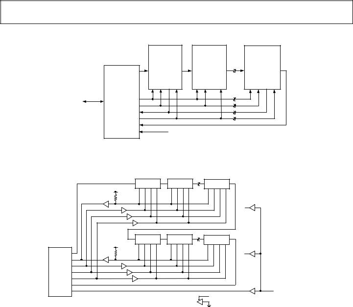
ADSP-21060/ADSP-21060L/ADSP-21062/ADSP-21062L/ADSP-21060C/ADSP-21060LC
|
|
ADSP-2106x |
|
JTAG |
|
ADSP-2106x |
||||||
|
|
|
|
#1 |
|
|
DEVICE |
|
|
|
n |
|
|
|
|
|
|
|
(OPTIONAL) |
|
|
|
|
||
|
TDI |
TDI |
TMS |
EMU |
TDO |
TDI |
TMS |
TDO |
TDI |
TMS |
EMU |
TDO |
|
JTAG |
TCK |
TRST |
TCK |
TRST |
TCK |
TRST |
|||||
|
EZ-ICE |
|
|
|
|
|
|
|
|
|
|
|
|
CONNECTOR |
|
|
|
|
|
|
|
|
|
|
|
OTHER |
TCK |
|
|
|
|
|
|
|
|
|
|
|
JTAG |
|
|
|
|
|
|
|
|
|
|
|
|
TMS |
|
|
|
|
|
|
|
|
|
|
|
|
CONTROLLER |
|
|
|
|
|
|
|
|
|
|
|
|
|
EMU |
|
|
|
|
|
|
|
|
|
|
|
|
TRST |
|
|
|
|
|
|
|
|
|
|
|
|
TDO |
|
|
|
|
|
|
|
|
|
|
|
|
CLKIN |
OPTIONAL |
|
|
|
|
|
|
|
|
||
|
|
|
|
|
|
|
|
|
|
|||
Figure 6. JTAG Scan Path Connections for Multiple ADSP-2106x Systems
|
|
TDI |
TDO |
TDI |
TDO |
TDI |
TDO |
|
* |
5kV |
|
|
|
|
|
|
|
|
|
|
|
|
|
|
|
TDI |
TDO |
TDI |
TDO |
TDI |
TDO |
TDI |
* |
5kV |
|
|
|
|
|
EMU |
|
|
|
|
|
|
|
|
|
|
|
|
|
|
|
TCK |
|
|
|
|
|
|
|
TMS |
|
|
|
|
|
|
|
TRST |
|
|
|
|
|
|
|
TDO |
|
|
|
|
|
|
|
CLKIN |
|
|
|
|
|
|
SYSTEM |
|
|
|
|
|
|
CLKIN |
|
|
|
|
|
|
|
EMU |
|
|
|
|
|
|
|
|
*OPEN-DRAIN DRIVER OR EQUIVALENT, i.e.,
Figure 7. JTAG Clocktree for Multiple ADSP-2106x Systems
Rev. G | Page 14 of 64 | August 2010
ADSP-21060/ADSP-21060L/ADSP-21062/ADSP-21062L/ADSP-21060C/ADSP-21060LC
ADSP-21060/ADSP-21062 SPECIFICATIONS
Note that component specifications are subject to change without notice.
OPERATING CONDITIONS (5 V)
|
|
|
A Grade |
|
C Grade |
|
K Grade |
|
Parameter |
Description |
Min |
Max |
Min |
Max |
Min |
Max |
Unit |
|
|
|
|
|
|
|
|
|
VDD |
Supply Voltage |
4.75 |
5.25 |
4.75 |
5.25 |
4.75 |
5.25 |
V |
TCASE |
Case Operating Temperature |
–40 |
+85 |
–40 |
+100 |
–40 |
+85 |
°C |
VIH11 |
High Level Input Voltage @ VDD = Max |
2.0 |
VDD + 0.5 |
2.0 |
VDD + 0.5 |
2.0 |
VDD + 0.5 |
V |
VIH22 |
High Level Input Voltage @ VDD = Max |
2.2 |
VDD + 0.5 |
2.2 |
VDD + 0.5 |
2.2 |
VDD + 0.5 |
V |
VIL 1, 2 |
Low Level Input Voltage @ VDD = Min |
–0.5 |
+0.8 |
–0.5 |
+0.8 |
–0.5 |
+0.8 |
V |
1Applies to input and bidirectional pins: DATA47–0, ADDR31–0, RD, WR, SW, ACK, SBTS, IRQ2–0, FLAG3–0, HGB, CS, DMAR1, DMAR2, BR6–1, ID2–0, RPBA, CPA, TFS0, TFS1, RFS0, RFS1, LxDAT3–0, LxCLK, LxACK, EBOOT, LBOOT, BMS, TMS, TDI, TCK, HBR, DR0, DR1, TCLK0, TCLK1, RCLK0, RCLK1.
2 Applies to input pins: CLKIN, RESET, TRST.
ELECTRICAL CHARACTERISTICS (5 V)
Parameter |
Description |
Test Conditions |
Min |
Max |
Unit |
|
|
|
|
|
|
VOH1, 2 |
High Level Output Voltage |
@ VDD = Min, IOH = –2.0 mA |
4.1 |
|
V |
VOL1, 2 |
Low Level Output Voltage |
@ VDD = Min, IOL = 4.0 mA |
|
0.4 |
V |
IIH3, 4 |
High Level Input Current |
@ VDD = Max, VIN = VDD Max |
|
10 |
μA |
IIL3 |
Low Level Input Current |
@ VDD = Max, VIN = 0 V |
|
10 |
μA |
IILP4 |
Low Level Input Current |
@ VDD = Max, VIN = 0 V |
|
150 |
μA |
5, 6, 7, 8 |
Three-State Leakage Current |
@ VDD = Max, VIN = VDD Max |
|
10 |
μA |
IOZH |
|
||||
IOZL5, 9 |
Three-State Leakage Current |
@ VDD = Max, VIN = 0 V |
|
10 |
μA |
9 |
Three-State Leakage Current |
@ VDD = Max, VIN = VDD Max |
|
350 |
μA |
IOZHP |
|
||||
7 |
Three-State Leakage Current |
@ VDD = Max, VIN = 0 V |
|
1.5 |
mA |
IOZLC |
|
||||
10 |
Three-State Leakage Current |
@ VDD = Max, VIN = 1.5 V |
|
350 |
μA |
IOZLA |
|
||||
8 |
Three-State Leakage Current |
@ VDD = Max, VIN = 0 V |
|
4.2 |
mA |
IOZLAR |
|
||||
6 |
Three-State Leakage Current |
@ VDD = Max, VIN = 0 V |
|
150 |
μA |
IOZLS |
|
||||
CIN11, 12 |
Input Capacitance |
fIN = 1 MHz, TCASE = 25°C, VIN = 2.5 V |
|
4.7 |
pF |
1Applies to output and bidirectional pins: DATA47–0, ADDR31-0, MS3–0, RD, WR, PAGE, ADRCLK, SW, ACK, FLAG3–0, TIMEXP, HBG, REDY, DMAG1, DMAG2, BR6–1, CPA, DT0, DT1, TCLK0, TCLK1, RCLK0, RCLK1, TFS0, TFS1, RFS0, RFS1, LxDAT3–0, LxCLK, LxACK, BMS, TDO, EMU, ICSA.
2 See “Output Drive Currents” for typical drive current capabilities.
3 Applies to input pins: ACK, SBTS, IRQ2–0, HBR, CS, DMAR1, DMAR2, ID2–0, RPBA, EBOOT, LBOOT, CLKIN, RESET, TCK.
4 Applies to input pins with internal pull-ups: DR0, DR1, TRST, TMS, TDI.
5Applies to three-statable pins: DATA47–0, ADDR31–0, MS3–0, RD, WR, PAGE, ADRCLK, SW, ACK, FLAG3–0, HBG, REDY, DMAG1, DMAG2, BMS, BR6–1, TFSx, RFSx, TDO, EMU. (Note that ACK is pulled up internally with 2 kΩ during reset in a multiprocessor system, when ID2–0 = 001 and another ADSP-2106x is not requesting bus mastership.)
6 Applies to three-statable pins with internal pull-ups: DT0, DT1, TCLK0, TCLK1, RCLK0, RCLK1. 7 Applies to CPA pin.
8Applies to ACK pin when pulled up. (Note that ACK is pulled up internally with 2 kΩ during reset in a multiprocessor system, when ID2–0 = 001 and another ADSP-2106xL is not requesting bus mastership).
9 Applies to three-statable pins with internal pull-downs: LxDAT3–0, LxCLK, LxACK. 10Applies to ACK pin when keeper latch enabled.
11Applies to all signal pins.
12Guaranteed but not tested.
Rev. G | Page 15 of 64 | August 2010

ADSP-21060/ADSP-21060L/ADSP-21062/ADSP-21062L/ADSP-21060C/ADSP-21060LC
INTERNAL POWER DISSIPATION (5 V)
These specifications apply to the internal power portion of VDD only. For a complete discussion of the code used to measure power dissipation, see the technical note “SHARC Power Dissipation Measurements.”
Specifications are based on the operating scenarios.
Operation |
Peak Activity (IDDINPEAK) |
High Activity (IDDINHIGH) |
Low Activity (IDDINLOW) |
Instruction Type |
Multifunction |
Multifunction |
Single Function |
Instruction Fetch |
Cache |
Internal Memory |
Internal Memory |
Core memory Access |
2 Per Cycle (DM and PM) |
1 Per Cycle (DM) |
None |
Internal Memory DMA |
1 Per Cycle |
1 Per 2 Cycles |
1 Per 2 Cycles |
To estimate power consumption for a specific application, use the following equation where% is the amount of time your program spends in that state:
%PEAK IDDINPEAK +%HIGH IDDINHIGH +%LOW IDDINLOW +
%IDLE IDDIDLE = Power Consumption
Parameter |
Test Conditions |
Max |
Units |
IDDINPEAK Supply Current (Internal)1 |
tCK = 30 ns, VDD = Max |
745 |
mA |
|
tCK = 25 ns, VDD = Max |
850 |
mA |
IDDINHIGH Supply Current (Internal)2 |
tCK = 30 ns, VDD = Max |
575 |
mA |
|
tCK = 25 ns, VDD = Max |
670 |
mA |
IDDINLOW Supply Current (Internal)2 |
tCK = 30 ns, VDD = Max |
340 |
mA |
|
tCK = 25 ns, VDD = Max |
390 |
mA |
IDDIDLE Supply Current (Idle)3 |
VDD = Max |
200 |
mA |
1The test program used to measure IDDINPEAK represents worst case processor operation and is not sustainable under normal application conditions. Actual internal power measurements made using typical applications are less than specified.
2 IDDINHIGH is a composite average based on a range of high activity code. IDDINLOW is a composite average based on a range of low activity code. 3 Idle denotes ADSP-2106x state during execution of IDLE instruction.
Rev. G | Page 16 of 64 | August 2010

ADSP-21060/ADSP-21060L/ADSP-21062/ADSP-21062L/ADSP-21060C/ADSP-21060LC
EXTERNAL POWER DISSIPATION (5 V)
Total power dissipation has two components, one due to internal circuitry and one due to the switching of external output drivers. Internal power dissipation is dependent on the instruction execution sequence and the data operands involved. Internal power dissipation is calculated in the following way:
PINT = IDDIN × VDD
The external component of total power dissipation is caused by the switching of output pins. Its magnitude depends on:
•the number of output pins that switch during each cycle
(O)
•the maximum frequency at which they can switch (f)
•their load capacitance (C)
•their voltage swing (VDD)
and is calculated by:
PEXT = O × C × VDD2 × f
The load capacitance should include the processor’s package capacitance (CIN). The switching frequency includes driving the load high and then back low. Address and data pins can
Table 5. External Power Calculations (5 V Devices)
drive high and low at a maximum rate of 1/(2tCK). The write strobe can switch every cycle at a frequency of 1/tCK. Select pins switch at 1/(2tCK), but selects can switch on each cycle.
Example: Estimate PEXT with the following assumptions:
•A system with one bank of external data memory RAM (32-bit)
•Four 128K × 8 RAM chips are used, each with a load of 10 pF
•External data memory writes occur every other cycle, a rate of 1/(4tCK), with 50% of the pins switching
•The instruction cycle rate is 40 MHz (tCK = 25 ns)
The PEXT equation is calculated for each class of pins that can drive:
A typical power consumption can now be calculated for these conditions by adding a typical internal power dissipation:
PTOTAL = PEXT + (IDDIN2 × 5.0 V)
Note that the conditions causing a worst-case PEXT are different from those causing a worst-case PINT. Maximum PINT cannot occur while 100% of the output pins are switching from all ones to all zeros. Note also that it is not common for an application to have 100% or even 50% of the outputs switching simultaneously.
|
|
Pin Type |
No. of Pins |
% Switching |
× C |
× f |
× VDD2 |
= PEXT |
||
|
|
Address |
15 |
50 |
× 44.7 pF |
× 10 MHz |
× 25 V |
= 0.084 W |
||
|
|
|
|
|
1 |
0 |
× 44.7 pF |
× 10 MHz |
× 25 V |
= 0.000 W |
MS0 |
||||||||||
|
|
|
1 |
– |
× 44.7 pF |
× 20 MHz |
× 25 V |
= 0.022 W |
||
|
WR |
|||||||||
|
Data |
32 |
50 |
× 14.7 pF |
× 10 MHz |
× 25 V |
= 0.059 W |
|||
ADDRCLK |
1 |
– |
× 4.7 pF |
× 20 MHz |
× 25 V |
= 0.002 W |
||||
PEXT = 0.167 W
Rev. G | Page 17 of 64 | August 2010

ADSP-21060/ADSP-21060L/ADSP-21062/ADSP-21062L/ADSP-21060C/ADSP-21060LC
ADSP-21060L/ADSP-21062L SPECIFICATIONS
Note that component specifications are subject to change without notice.
OPERATING CONDITIONS (3.3 V)
|
|
|
A Grade |
|
C Grade |
|
K Grade |
|
Parameter |
Description |
Min |
Max |
Min |
Max |
Min |
Max |
Unit |
|
|
|
|
|
|
|
|
|
VDD |
Supply Voltage |
3.15 |
3.45 |
3.15 |
3.45 |
3.15 |
3.45 |
V |
TCASE |
Case Operating Temperature |
–40 |
+85 |
–40 |
+100 |
–40 |
+85 |
°C |
VIH11 |
High Level Input Voltage @ VDD = Max |
2.0 |
VDD + 0.5 |
2.0 |
VDD + 0.5 |
2.0 |
VDD + 0.5 |
V |
VIH22 |
High Level Input Voltage @ VDD = Max |
2.2 |
VDD + 0.5 |
2.2 |
VDD + 0.5 |
2.2 |
VDD + 0.5 |
V |
VIL 1, 2 |
Low Level Input Voltage @ VDD = Min |
–0.5 |
+0.8 |
–0.5 |
+0.8 |
–0.5 |
+0.8 |
V |
1Applies to input and bidirectional pins: DATA47–0, ADDR31–0, RD, WR, SW, ACK, SBTS, IRQ2–0, FLAG3–0, HGB, CS, DMAR1, DMAR2, BR6–1, ID2–0, RPBA, CPA, TFS0, TFS1, RFS0, RFS1, LxDAT3–0, LxCLK, LxACK, EBOOT, LBOOT, BMS, TMS, TDI, TCK, HBR, DR0, DR1, TCLK0, TCLK1, RCLK0, RCLK1
2 Applies to input pins: CLKIN, RESET, TRST
ELECTRICAL CHARACTERISTICS (3.3 V)
Parameter |
Description |
Test Conditions |
Min |
Max |
Unit |
|
|
|
|
|
|
VOH1, 2 |
High Level Output Voltage |
@ VDD = Min, IOH = –2.0 mA |
2.4 |
|
V |
VOL1, 2 |
Low Level Output Voltage |
@ VDD = Min, IOL = 4.0 mA |
|
0.4 |
V |
IIH3, 4 |
High Level Input Current |
@ VDD = Max, VIN = VDD Max |
|
10 |
μA |
IIL3 |
Low Level Input Current |
@ VDD = Max, VIN = 0 V |
|
10 |
μA |
IILP4 |
Low Level Input Current |
@ VDD = Max, VIN = 0 V |
|
150 |
μA |
5, 6, 7, 8 |
Three-State Leakage Current |
@ VDD = Max, VIN = VDD Max |
|
10 |
μA |
IOZH |
|
||||
IOZL5, 9 |
Three-State Leakage Current |
@ VDD = Max, VIN = 0 V |
|
10 |
μA |
9 |
Three-State Leakage Current |
@ VDD = Max, VIN = VDD Max |
|
350 |
μA |
IOZHP |
|
||||
7 |
Three-State Leakage Current |
@ VDD = Max, VIN = 0 V |
|
1.5 |
mA |
IOZLC |
|
||||
10 |
Three-State Leakage Current |
@ VDD = Max, VIN = 1.5 V |
|
350 |
μA |
IOZLA |
|
||||
8 |
Three-State Leakage Current |
@ VDD = Max, VIN = 0 V |
|
4.2 |
mA |
IOZLAR |
|
||||
6 |
Three-State Leakage Current |
@ VDD = Max, VIN = 0 V |
|
150 |
μA |
IOZLS |
|
||||
CIN11, 12 |
Input Capacitance |
fIN = 1 MHz, TCASE = 25°C, VIN = 2.5 V |
|
4.7 |
pF |
1Applies to output and bidirectional pins: DATA47–0, ADDR31–0, MS3–0, RD, WR, PAGE, ADRCLK, SW, ACK, FLAG3–0, TIMEXP, HBG, REDY, DMAG1, DMAG2, BR6–1, CPA, DT0, DT1, TCLK0, TCLK1, RCLK0, RCLK1, TFS0, TFS1, RFS0, RFS1, LxDAT3–0, LxCLK, LxACK, BMS, TDO, EMU, ICSA.
2 See “Output Drive Currents” for typical drive current capabilities.
3 Applies to input pins: ACK, SBTS, IRQ2–0, HBR, CS, DMAR1, DMAR2, ID2–0, RPBA, EBOOT, LBOOT, CLKIN, RESET, TCK.
4 Applies to input pins with internal pull-ups: DR0, DR1, TRST, TMS, TDI.
5Applies to three-statable pins: DATA47–0, ADDR31–0, MS3–0, RD, WR, PAGE, ADRCLK, SW, ACK, FLAG3–0, HBG, REDY, DMAG1, DMAG2, BMS, BR6–1, TFSx, RFSx, TDO, EMU. (Note that ACK is pulled up internally with 2 kΩ during reset in a multiprocessor system, when ID2–0 = 001 and another ADSP-2106x is not requesting bus mastership.)
6 Applies to three-statable pins with internal pull-ups: DT0, DT1, TCLK0, TCLK1, RCLK0, RCLK1. 7 Applies to CPA pin.
8Applies to ACK pin when pulled up. (Note that ACK is pulled up internally with 2 kΩ during reset in a multiprocessor system, when ID2–0 = 001 and another ADSP-2106xL is not requesting bus mastership).
9 Applies to three-statable pins with internal pull-downs: LxDAT3–0, LxCLK, LxACK. 10Applies to ACK pin when keeper latch enabled.
11Applies to all signal pins.
12Guaranteed but not tested.
Rev. G | Page 18 of 64 | August 2010

ADSP-21060/ADSP-21060L/ADSP-21062/ADSP-21062L/ADSP-21060C/ADSP-21060LC
INTERNAL POWER DISSIPATION (3.3 V)
These specifications apply to the internal power portion of VDD only. For a complete discussion of the code used to measure power dissipation, see the technical note “SHARC Power Dissipation Measurements.”
Specifications are based on the operating scenarios.
Operation |
Peak Activity (IDDINPEAK) |
High Activity (IDDINHIGH) |
Low Activity (IDDINLOW) |
Instruction Type |
Multifunction |
Multifunction |
Single Function |
Instruction Fetch |
Cache |
Internal Memory |
Internal Memory |
Core memory Access |
2 Per Cycle (DM and PM) |
1 Per Cycle (DM) |
None |
Internal Memory DMA |
1 Per Cycle |
1 Per 2 Cycles |
1 Per 2 Cycles |
To estimate power consumption for a specific application, use the following equation where % is the amount of time your program spends in that state:
%PEAK IDDINPEAK + %HIGH IDDINHIGH + %LOW IDDINLOW +
%IDLE IDDIDLE = Power Consumption
Parameter |
Test Conditions |
Max |
Units |
IDDINPEAK Supply Current (Internal)1 |
tCK = 30 ns, VDD = Max |
540 |
mA |
|
tCK = 25 ns, VDD = Max |
600 |
mA |
IDDINHIGH Supply Current (Internal)2 |
tCK = 30 ns, VDD = Max |
425 |
mA |
|
tCK = 25 ns, VDD = Max |
475 |
mA |
IDDINLOW Supply Current (Internal)2 |
tCK = 30 ns, VDD = Max |
250 |
mA |
|
tCK = 25 ns, VDD = Max |
275 |
mA |
IDDIDLE Supply Current (Idle)3 |
VDD = Max |
180 |
mA |
1The test program used to measure IDDINPEAK represents worst case processor operation and is not sustainable under normal application conditions. Actual internal power measurements made using typical applications are less than specified.
2 IDDINHIGH is a composite average based on a range of high activity code. IDDINLOW is a composite average based on a range of low activity code. 3 Idle denotes ADSP-2106xL state during execution of IDLE instruction.
Rev. G | Page 19 of 64 | August 2010

ADSP-21060/ADSP-21060L/ADSP-21062/ADSP-21062L/ADSP-21060C/ADSP-21060LC
EXTERNAL POWER DISSIPATION (3.3 V)
Total power dissipation has two components, one due to internal circuitry and one due to the switching of external output drivers. Internal power dissipation is dependent on the instruction execution sequence and the data operands involved. Internal power dissipation is calculated in the following way:
PINT = IDDIN × VDD
The external component of total power dissipation is caused by the switching of output pins. Its magnitude depends on:
•the number of output pins that switch during each cycle
(O)
•the maximum frequency at which they can switch (f)
•their load capacitance (C)
•their voltage swing (VDD)
and is calculated by:
PEXT = O × C × VDD2 × f
The load capacitance should include the processor’s package capacitance (CIN). The switching frequency includes driving the load high and then back low. Address and data pins can
Table 6. External Power Calculations (3.3 V Devices)
drive high and low at a maximum rate of 1/(2tCK). The write strobe can switch every cycle at a frequency of 1/tCK. Select pins switch at 1/(2tCK), but selects can switch on each cycle.
Example: Estimate PEXT with the following assumptions:
•A system with one bank of external data memory RAM (32-bit)
•Four 128K × 8 RAM chips are used, each with a load of 10 pF
•External data memory writes occur every other cycle, a rate of 1/(4tCK), with 50% of the pins switching
•The instruction cycle rate is 40 MHz (tCK = 25 ns)
The PEXT equation is calculated for each class of pins that can drive:
A typical power consumption can now be calculated for these conditions by adding a typical internal power dissipation:
PTOTAL = PEXT + (IDDIN2 × 5.0 V)
Note that the conditions causing a worst-case PEXT are different from those causing a worst-case PINT. Maximum PINT cannot occur while 100% of the output pins are switching from all ones to all zeros. Note also that it is not common for an application to have 100% or even 50% of the outputs switching simultaneously.
|
|
Pin Type |
No. of Pins |
% Switching |
× C |
× f |
× VDD2 |
= PEXT |
||
|
|
Address |
15 |
50 |
× 44.7 pF |
× 10 MHz |
× 10.9 V |
= 0.037 W |
||
|
|
|
|
|
1 |
0 |
× 44.7 pF |
× 10 MHz |
× 10.9 V |
= 0.000 W |
MS0 |
||||||||||
|
|
|
1 |
– |
× 44.7 pF |
× 20 MHz |
× 10.9 V |
= 0.010 W |
||
|
WR |
|||||||||
|
Data |
32 |
50 |
× 14.7 pF |
× 10 MHz |
× 10.9 V |
= 0.026 W |
|||
ADDRCLK |
1 |
– |
× 4.7 pF |
× 20 MHz |
× 10.9 V |
= 0.001 W |
||||
PEXT = 0.074 W
ABSOLUTE MAXIMUM RATINGS
Stresses greater than those listed Table 7 may cause permanent damage to the device. These are stress ratings only; functional operation of the device at these or any other conditions greater
Table 7. Absolute Maximum Ratings
than those indicated in the operational sections of this specification is not implied. Exposure to absolute maximum rating conditions for extended periods may affect device reliability.
|
ADSP-21060/ADSP-21060C |
ADSP-21060L/ADSP-21060LC |
|
ADSP-21062 |
ADSP-21062L |
Parameter |
5 V |
3.3 V |
Supply Voltage (VDD) |
–0.3 V to +7.0 V |
–0.3 V to +4.6 V |
Input Voltage |
–0.5 V to VDD + 0.5 V |
–0.5 V to VDD +0.5 V |
Output Voltage Swing |
–0.5 V to VDD + 0.5 V |
–0.5 V to VDD + 0.5 V |
Load Capacitance |
200 pF |
200 pF |
Storage Temperature Range |
–65°C to +150°C |
–65°C to +150°C |
Lead Temperature (5 seconds) |
280°C |
280°C |
Junction Temperature Under Bias |
130°C |
130°C |
Rev. G | Page 20 of 64 | August 2010
Loading...