


 Loading...
Analog Devices ADM695SQ, ADM695AR, ADM695AQ, ADM695AN, ADM694SQ Datasheet
...
a |
Microprocessor |
|
Supervisory Circuits |
||
|
|
|
|
|
ADM690–ADM695 |
|
|
|
FEATURES
Superior Upgrade for MAX690–MAX695 Specified Over Temperature
Low Power Consumption (5 mW) Precision Voltage Monitor
Reset Assertion Down to 1 V VCC
Low Switch On-Resistance 1.5 V Normal, 20 V in Backup
High Current Drive (100 mA)
Watchdog Timer—100 ms, 1.6 s, or Adjustable 600 nA Standby Current
Automatic Battery Backup Power Switching Extremely Fast Gating of Chip Enable Signals (5 ns) Voltage Monitor for Power Fail
APPLICATIONS
Microprocessor Systems
Computers
Controllers
Intelligent Instruments
Automotive Systems
GENERAL DESCRIPTION
The ADM690–ADM695 family of supervisory circuits offers complete single chip solutions for power supply monitoring and battery control functions in microprocessor systems. These functions include μP reset, backup battery switchover, watchdog timer, CMOS RAM write protection, and power failure warning. The complete family provides a variety of configurations to satisfy most microprocessor system requirements.
The ADM690, ADM692 and ADM694 are available in 8-pin DIP packages and provide:
1.Power-on reset output during power-up, power-down and brownout conditions. The RESET output remains operational with VCC as low as 1 V.
2.Battery backup switching for CMOS RAM, CMOS microprocessor or other low power logic.
3.A reset pulse if the optional watchdog timer has not been toggled within a specified time.
4.A 1.3 V threshold detector for power fail warning, low battery detection, or to monitor a power supply other than +5 V.
The ADM691, ADM693 and ADM695 are available in 16-pin DIP and small outline packages and provide three additional functions.
1.Write protection of CMOS RAM or EEPROM.
2.Adjustable reset and watchdog timeout periods.
3.Separate watchdog timeout, backup battery switchover, and low VCC status outputs.
REV. A
Information furnished by Analog Devices is believed to be accurate and reliable. However, no responsibility is assumed by Analog Devices for its use, nor for any infringements of patents or other rights of third parties which may result from its use. No license is granted by implication or otherwise under any patent or patent rights of Analog Devices.
FUNCTIONAL BLOCK DIAGRAMS
VBATT |
|
|
|
|
|
|
|
|
VOUT |
VCC |
|
|
|
|
|
4.65V1 |
RESET |
|
|
|
GENERATOR2 |
RESET |
||
WATCHDOG |
WATCHDOG |
|
ADM690 |
|
TRANSITION DETECTOR |
|
|||
INPUT (WDI) |
(1.6s) |
|
ADM692 |
|
POWER FAIL |
|
|
ADM694 |
|
|
|
|
|
|
INPUT (PFI) |
|
|
|
POWER FAIL |
|
1.3V |
|
|
OUTPUT (PFO) |
|
|
|
|
|
|
1VOLTAGE DETECTOR = 4.65V (ADM690, ADM694) |
|
||
|
|
4.40V (ADM692) |
|
|
2RESET PULSE WIDTH = 50ms (ADM690, ADM692) 200ms (ADM694)
BATT ON
VBATT |
|
|
|
|
|
|
|
|
|
VOUT |
|
|
|
|
ADM691 |
|
|
VCC |
|
|
ADM693 |
|
|
CEIN |
|
|
ADM695 |
|
|
|
|
|
CEOUT |
||
|
|
|
|
||
|
4.65V1 |
|
|
LOW LINE |
|
|
|
|
|
||
|
|
|
|
RESET |
|
OSC IN |
RESET & |
RESET |
|
|
|
|
WATCHDOG |
|
RESET |
||
OSC SEL |
GENERATOR |
||||
TIMEBASE |
|
||||
|
|
|
|||
WATCHDOG |
WATCHDOG |
|
WATCHDOG |
WATCHDOG |
|
TRANSITION DETECTOR |
TIMER |
||||
INPUT (WDI) |
OUTPUT (WDO) |
||||
|
|
|
|||
POWER FAIL |
|
|
|
|
|
INPUT (PFI) |
|
|
|
POWER FAIL |
|
|
1.3V |
|
|
OUTPUT (PFO) |
|
|
|
|
|
||
|
1VOLTAGE DETECTOR = 4.65V (ADM691, ADM695) |
|
|||
|
|
4.40V (ADM693) |
|
||
The ADM690–ADM695 family is fabricated using an advanced epitaxial CMOS process combining low power consumption
(5 mW), extremely fast Chip Enable gating (5 ns) and high reliability. RESET assertion is guaranteed with VCC as low as 1 V. In addition, the power switching circuitry is designed for minimal voltage drop thereby permitting increased output current drive of up to 100 mA without the need for an external pass transistor.
© Analog Devices, Inc., 1996
One Technology Way, P.O. Box 9106, Norwood, MA 02062-9106, U.S.A. Tel: 617/329-4700 Fax: 617/326-8703
ADM690–ADM695–SPECIFICATIONS |
(VCC = Full Operating Range, VBATT = +2.8 V, TA = TMIN to |
|||||||||||||||||
TMAX unless otherwise noted) |
||||||||||||||||||
Parameter |
Min |
Typ |
Max |
Units |
Test Conditions/Comments |
|||||||||||||
|
|
|
|
|
|
|
|
|
|
|
|
|
|
|
|
|
|
|
BATTERY BACKUP SWITCHING |
|
|
|
|
|
|
|
|
|
|||||||||
|
VCC Operating Voltage Range |
|
|
|
|
|
|
|
|
|
||||||||
|
ADM690, ADM691, ADM694, ADM695 |
4.75 |
|
5.5 |
V |
|
|
|
|
|
||||||||
|
ADM692, ADM693 |
4.5 |
|
5.5 |
V |
|
|
|
|
|
||||||||
|
VBATT Operating Voltage Range |
|
|
|
|
|
|
|
|
|
||||||||
|
ADM690, ADM691, ADM694, ADM695 |
2.0 |
|
4.25 |
V |
|
|
|
|
|
||||||||
|
ADM692, ADM693 |
2.0 |
|
4.0 |
V |
|
|
|
|
|
||||||||
|
VOUT Output Voltage |
VCC – 0.05 |
VCC – 0.025 |
|
V |
IOUT = 1 mA |
||||||||||||
|
|
|
|
|
|
|
|
|
|
VCC – 0.5 |
VCC – 0.25 |
|
V |
IOUT ≤ 100 mA |
||||
|
VOUT in Battery Backup Mode |
VBATT – 0.05 |
VBATT – 0.02 |
|
V |
IOUT = 250 μA, VCC < VBATT – 0.2 V |
||||||||||||
|
Supply Current (Excludes IOUT) |
|
1 |
1.95 |
mA |
IOUT = 100 mA |
||||||||||||
|
Supply Current in Battery Backup Mode |
|
0.6 |
1 |
μA |
VCC = 0 V, VBATT = 2.8 V |
||||||||||||
|
Battery Standby Current |
|
|
|
μA |
5.5 V > VCC > VBATT + 0.2 V |
||||||||||||
|
(+ = Discharge, – = Charge) |
–0.1 |
|
+0.02 |
TA = +25°C |
|||||||||||||
|
|
|
|
|
|
|
|
|
|
–1.0 |
|
+0.02 |
μA |
|
|
|
|
|
|
Battery Switchover Threshold |
|
70 |
|
mV |
Power Up |
||||||||||||
|
VCC – VBATT |
|
50 |
|
mV |
Power Down |
||||||||||||
|
Battery Switchover Hysteresis |
|
20 |
|
mV |
|
|
|
|
|
||||||||
|
BATT ON Output Voltage |
|
|
0.3 |
V |
ISINK = 3.2 mA |
||||||||||||
|
BATT ON Output Short Circuit Current |
|
35 |
|
mA |
BATT ON = VOUT = 4.5 V Sink Current |
||||||||||||
|
|
|
|
|
|
|
|
|
|
0.5 |
1 |
25 |
μA |
BATT ON = 0 V Source Current |
||||
RESET AND WATCHDOG TIMER |
|
|
|
|
|
|
|
|
|
|||||||||
|
Reset Voltage Threshold |
|
|
|
|
|
|
|
|
|
||||||||
|
ADM690, ADM691, ADM694, ADM695 |
4.5 |
4.65 |
4.73 |
V |
|
|
|
|
|
||||||||
|
ADM692, ADM693 |
4.25 |
4.4 |
4.48 |
V |
|
|
|
|
|
||||||||
|
Reset Threshold Hysteresis |
|
40 |
|
mV |
|
|
|
|
|
||||||||
|
Reset Timeout Delay |
|
|
|
|
OSC SEL = HIGH, VCC = 5 V, TA = +25°C |
||||||||||||
|
ADM690, ADM691, ADM692, ADM693 |
35 |
50 |
70 |
ms |
|||||||||||||
|
ADM694, ADM695 |
140 |
200 |
280 |
ms |
OSC SEL = HIGH, VCC = 5 V, TA = +25°C |
||||||||||||
|
Watchdog Timeout Period, Internal Oscillator |
1.0 |
1.6 |
2.25 |
s |
Long Period, VCC = 5 V, TA = +25°C |
||||||||||||
|
|
|
|
|
|
|
|
|
|
70 |
100 |
140 |
ms |
Short Period, VCC = 5 V, TA = +25°C |
||||
|
Watchdog Timeout Period, External Clock |
3840 |
|
4097 |
Cycles |
Long Period |
||||||||||||
|
|
|
|
|
|
|
|
|
|
768 |
|
1025 |
Cycles |
Short Period |
||||
|
Minimum WDI Input Pulse Width |
50 |
|
|
ns |
VIL = 0.4, VIH = 3.5 V |
||||||||||||
|
|
|
|
Output Voltage @ VCC = +1 V |
|
4 |
200 |
mV |
ISINK = 10 μA, VCC = 1 V |
|||||||||
|
RESET |
|
||||||||||||||||
|
RESET |
, |
LOW |
|
|
LINE |
Output Voltage |
|
|
0.4 |
V |
ISINK = 1.6 mA, VCC = 4.25 V |
||||||
|
|
|
|
|
|
|
|
|
|
3.5 |
|
|
V |
ISOURCE = 1 μA, VCC = 5 V |
||||
|
RESET |
, |
WDO |
Output Voltage |
|
|
0.4 |
V |
ISINK = 1.6 mA, VCC = 5 V |
|||||||||
|
|
|
|
|
|
|
|
|
|
3.5 |
|
|
V |
ISOURCE = 1 μA, VCC = 4.25 V |
||||
|
Output Short Circuit Source Current |
1 |
3 |
25 |
μA |
|
|
|
|
|
||||||||
|
Output Short Circuit Sink Current |
|
25 |
|
mA |
|
|
|
|
|
||||||||
|
WDI Input Threshold |
|
|
|
|
VCC = 5 V1 |
||||||||||||
|
Logic Low |
|
|
0.8 |
V |
|
|
|
|
|
||||||||
|
Logic High |
3.5 |
|
|
V |
|
|
|
|
|
||||||||
|
WDI Input Current |
|
20 |
50 |
μA |
WDI = VOUT, TA = +25°C |
||||||||||||
|
|
|
|
|
|
|
|
|
|
–50 |
–15 |
|
μA |
WDI = 0 V, TA = +25°C |
||||
POWER FAIL DETECTOR |
|
|
|
|
|
|
|
|
|
|||||||||
|
PFI Input Threshold |
1.25 |
1.3 |
1.35 |
V |
VCC = +5 V |
||||||||||||
|
PFI Input Current |
–25 |
±0.01 |
+25 |
nA |
|
|
|
|
|
||||||||
|
PFO |
Output Voltage |
|
|
0.4 |
V |
ISINK = 3.2 mA |
|||||||||||
|
|
|
|
|
|
|
|
|
|
3.5 |
|
|
V |
ISOURCE = 1 μA |
||||
|
|
|
Short Circuit Source Current |
1 |
3 |
25 |
μA |
PFI = Low, |
|
|
|
= 0 V |
||||||
|
PFO |
PFO |
||||||||||||||||
|
PFO |
Short Circuit Sink Current |
|
25 |
|
mA |
PFI = High, |
PFO |
= VOUT |
|||||||||
CHIP ENABLE GATING |
|
|
|
|
|
|
|
|
|
|||||||||
|
|
IN Threshold |
|
|
0.8 |
V |
VIL |
|||||||||||
|
CE |
|
|
|||||||||||||||
|
|
|
|
|
|
|
|
|
|
3.0 |
|
|
V |
VIH |
||||
|
|
IN Pull-Up Current |
|
3 |
|
μA |
|
|
|
|
|
|||||||
|
CE |
|
|
|
|
|
|
|
||||||||||
|
CE |
OUT Output Voltage |
|
|
0.4 |
V |
ISINK = 3.2 mA |
|||||||||||
|
|
|
|
|
|
|
|
|
|
VOUT – 1.5 |
|
|
V |
ISOURCE = 3.0 mA |
||||
|
|
|
|
|
|
|
|
|
|
VOUT – 0.05 |
|
|
V |
ISOURCE = 1 μA, VCC = 0 V |
||||
|
CE |
Propagation Delay |
|
5 |
9 |
ns |
|
|
|
|
|
|||||||
|
|
|
|
|
|
|
|
|
|
|
|
|
|
|
|
|
|
|
–2– |
REV. A |

ADM690–ADM695
Parameter |
Min |
Typ |
Max |
Units |
Test Conditions/Comments |
|
|
|
|
|
|
|
|
OSCILLATOR |
|
±2 |
|
μA |
|
|
OSC IN Input Current |
|
|
|
|
||
OSC SEL Input Pull-Up Current |
|
5 |
|
μA |
|
|
OSC IN Frequency Range |
0 |
|
250 |
kHz |
OSC SEL = 0 |
V |
OSC IN Frequency with External Capacitor |
|
4 |
|
kHz |
OSC SEL = 0 |
V, COSC = 47 pF |
NOTE
1WDI is a three level input which is internally biased to 38% of VCC and has an input impedance of approximately 125 kΩ. Specifications subject to change without notice.
ABSOLUTE MAXIMUM RATINGS*
(TA = +25°C unless otherwise noted)
VCC . . . . . . . . . . . . . . . . . . . . . . . . . . . |
. . . . . . . –0.3 V to +6 V |
VBATT . . . . . . . . . . . . . . . . . . . . . . . . . |
. . . . . . . –0.3 V to +6 V |
All Other Inputs . . . . . . . . . . . . . . . . . . |
–0.3 V to VOUT + 0.5 V |
Input Current |
|
VCC . . . . . . . . . . . . . . . . . . . . . . . . . . |
. . . . . . . . . . . 200 mA |
VBATT . . . . . . . . . . . . . . . . . . . . . . . . |
. . . . . . . . . . . . 50 mA |
GND . . . . . . . . . . . . . . . . . . . . . . . . . |
. . . . . . . . . . . . 20 mA |
Digital Output Current . . . . . . . . . . . . . |
. . . . . . . . . . . . 20 mA |
Power Dissipation, N-8 DIP . . . . . . . . . |
. . . . . . . . . . . 400 mW |
θJA Thermal Impedance . . . . . . . . . . . |
. . . . . . . . . . 120°C/W |
Power Dissipation, Q-8 DIP . . . . . . . . . |
. . . . . . . . . . . 500 mW |
θJA Thermal Impedance . . . . . . . . . . . |
. . . . . . . . . . 125°C/W |
Power Dissipation, N-16 DIP . . . . . . . . |
. . . . . . . . . . . 600 mW |
θJA Thermal Impedance . . . . . . . . . . . |
. . . . . . . . . . 135°C/W |
Power Dissipation, Q-16 DIP . . . . . . . . |
. . . . . . . . . . . 600 mW |
θJA Thermal Impedance . . . . . . . . . . . |
. . . . . . . . . . 100°C/W |
Power Dissipation, R-16 SOIC . . . . . . . |
. . . . . . . . . . . 600 mW |
θJA Thermal Impedance . . . . . . . . . . . |
. . . . . . . . . . 110°C/W |
Operating Temperature Range |
–40°C to +85°C |
Industrial (A Version) . . . . . . . . . . . . |
|
Extended (S Version) . . . . . . . . . . . . . |
. . . . –55°C to +125°C |
Lead Temperature (Soldering, 10 secs) . |
. . . . . . . . . . . +300°C |
Vapor Phase (60 secs) . . . . . . . . . . . . |
. . . . . . . . . . . +215°C |
Infrared (15 secs) . . . . . . . . . . . . . . . . |
. . . . . . . . . . . +220°C |
Storage Temperature Range . . . . . . . . . |
. . . . –65°C to +150°C |
*Stresses above those listed under “Absolute Maximum Ratings” may cause permanent damage to the device. This is a stress rating only and functional operation of the device at these or any other conditions above those listed in the operational sections of this specification is not implied. Exposure to absolute maximum ratings for extended periods of time may affect device reliability.
ORDERING GUIDE
Model |
Temperature Range |
Package Option |
|
|
|
ADM690AN |
–40°C to +85°C |
N-8 |
ADM690AQ |
–40°C to +85°C |
Q-8 |
ADM690SQ |
–55°C to +125°C |
Q-8 |
ADM691AN |
–40°C to +85°C |
N-16 |
ADM691AR |
–40°C to +85°C |
R-16 |
ADM691AQ |
–40°C to +85°C |
Q-16 |
ADM691SQ |
–55°C to +125°C |
Q-16 |
ADM692AN |
–40°C to +85°C |
N-8 |
ADM692AQ |
–40°C to +85°C |
Q-8 |
ADM692SQ |
–55°C to +125°C |
Q-8 |
ADM693AN |
–40°C to +85°C |
N-16 |
ADM693AR |
–40°C to +85°C |
R-16 |
ADM693AQ |
–40°C to +85°C |
Q-16 |
ADM693SQ |
–55°C to +125°C |
Q-16 |
ADM694AN |
–40°C to +85°C |
N-8 |
ADM694AQ |
–40°C to +85°C |
Q-8 |
ADM694SQ |
–55°C to +125°C |
Q-8 |
ADM695AN |
–40°C to +85°C |
N-16 |
ADM695AR |
–40°C to +85°C |
R-16 |
ADM695AQ |
–40°C to +85°C |
Q-16 |
ADM695SQ |
–55°C to +125°C |
Q-16 |
CAUTION
ESD (electrostatic discharge) sensitive device. Electrostatic charges as high as 4000 V readily accumulate on the human body and test equipment and can discharge without detection. Although the ADM690–ADM695 features proprietary ESD protection circuitry, permanent damage may occur on devices subjected to high energy electrostatic discharges. Therefore, proper ESD precautions are recommended to avoid performance degradation or loss of functionality.
WARNING!
ESD SENSITIVE DEVICE
REV. A |
–3– |
ADM690–ADM695
|
|
|
|
|
|
|
|
|
|
|
|
|
|
|
|
|
|
|
|
PIN FUNCTION DESCRIPTION |
|||||||||||||||||||
|
|
|
|
|
|
|
|
|
|
|
|
|
|
|
|
|
|
|
|
|
|
|
|
|
|
|
|
|
|
|
|
|
|
|
|
|
|
|
|
Mnemonic |
Function |
||||||||||||||||||||||||||||||||||||||
|
|
|
|
|
|
|
|
|
|
|
|
|
|
|
|
|
|
|
|
|
|
|
|
|
|
|
|
|
|
|
|
|
|
|
|
|
|
|
|
VCC |
Power Supply Input: +5 V Nominal. |
||||||||||||||||||||||||||||||||||||||
VBATT |
Backup Battery Input. Connect to Ground if a backup battery is not used. |
||||||||||||||||||||||||||||||||||||||
VOUT |
Output Voltage, VCC or VBATT is internally switched to VOUT depending on which is at the highest potential. VOUT |
||||||||||||||||||||||||||||||||||||||
|
|
|
|
|
|
|
can supply up to 100 mA to power CMOS RAM. Connect VOUT to VCC if VOUT and VBATT are not used. |
||||||||||||||||||||||||||||||||
GND |
0 V. Ground reference for all signals. |
||||||||||||||||||||||||||||||||||||||
|
|
|
|
|
|
|
Logic Output. |
|
|
|
|
goes low if |
|||||||||||||||||||||||||||
RESET |
RESET |
||||||||||||||||||||||||||||||||||||||
|
|
|
|
|
|
|
1. VCC falls below the Reset Threshold |
||||||||||||||||||||||||||||||||
|
|
|
|
|
|
|
2. VCC falls below VBATT |
||||||||||||||||||||||||||||||||
|
|
|
|
|
|
|
3. The watchdog timer is not serviced within its timeout period. |
||||||||||||||||||||||||||||||||
|
|
|
|
|
|
|
The reset threshold is typically 4.65 V for the ADM690/ADM691/ADM694/ADM695 and 4.4 V for the ADM692 and |
||||||||||||||||||||||||||||||||
|
|
|
|
|
|
|
ADM693. RESET remains low for 50 ms (ADM690/ADM691/ADM692/ADM693) or 200 ms (ADM694/ADM695) |
||||||||||||||||||||||||||||||||
|
|
|
|
|
|
|
after VCC returns above the threshold. |
RESET |
|
also goes low for 50 (200) ms if the watchdog timer is enabled but not |
|||||||||||||||||||||||||||||
|
|
|
|
|
|
|
serviced within its timeout period. The |
RESET |
pulse width can be adjusted on the ADM691/ADM693/ADM695 as |
||||||||||||||||||||||||||||||
|
|
|
|
|
|
|
shown in Table I. The RESET output has an internal 3 μA pull up, and can either connect to an open collector |
||||||||||||||||||||||||||||||||
|
|
|
|
|
|
|
Reset bus or directly drive a CMOS gate without an external pull-up resistor. |
||||||||||||||||||||||||||||||||
WDI |
Watchdog Input. WDI is a three level input. If WDI remains either high or low for longer than the watchdog timeout |
||||||||||||||||||||||||||||||||||||||
|
|
|
|
|
|
|
period, |
RESET |
pulses low and WDO goes low. The timer resets with each transition on the WDI line. The watchdog |
||||||||||||||||||||||||||||||
|
|
|
|
|
|
|
timer may be disabled if WDI is left floating or is driven to midsupply. |
||||||||||||||||||||||||||||||||
PFI |
Power Fail Input. PFI is the noninverting input to the Power Fail Comparator when PFI is less than 1.3 V, |
|
|
||||||||||||||||||||||||||||||||||||
PFO |
|||||||||||||||||||||||||||||||||||||||
|
|
|
|
|
|
|
goes low. Connect PFI to GND or VOUT when not used. |
||||||||||||||||||||||||||||||||
|
|
|
|
|
|
Power Fail Output. |
|
is the output of the Power Fail Comparator. It goes low when PFI is less than 1.3 V. The |
|||||||||||||||||||||||||||||||
PFO |
PFO |
||||||||||||||||||||||||||||||||||||||
|
|
|
|
|
|
|
comparator is turned off and |
PFO |
goes low when VCC is below VBATT. |
||||||||||||||||||||||||||||||
|
|
IN |
Logic Input. The input to the |
|
|
gating circuit. Connect to GND or VOUT if not used. |
|||||||||||||||||||||||||||||||||
CE |
CE |
||||||||||||||||||||||||||||||||||||||
|
OUT |
Logic Output. |
|
OUT is a gated version of the |
|
|
IN signal. |
|
OUT tracks |
|
|
IN when VCC is above the reset |
|||||||||||||||||||||||||||
CE |
CE |
CE |
CE |
CE |
|||||||||||||||||||||||||||||||||||
|
|
|
|
|
|
|
threshold. If VCC is below the reset threshold, |
CE |
OUT is forced high. See Figures 5 and 6. |
||||||||||||||||||||||||||||||
BATT ON |
Logic Output. BATT ON goes high when VOUT is internally switched to the VBATT input. It goes low when VOUT |
||||||||||||||||||||||||||||||||||||||
|
|
|
|
|
|
|
is internally switched to VCC. The output typically sinks 35 mA and can directly drive the base of an external |
||||||||||||||||||||||||||||||||
|
|
|
|
|
|
|
PNP transistor to increase the output current above the 100 mA rating of VOUT. |
||||||||||||||||||||||||||||||||
|
|
|
Logic Output. |
|
|
goes low when VCC falls below the reset threshold. It returns high as soon as VCC rises |
|||||||||||||||||||||||||||||||||
LOW LINE |
LOW LINE |
||||||||||||||||||||||||||||||||||||||
|
|
|
|
|
|
|
above the reset threshold. |
||||||||||||||||||||||||||||||||
RESET |
Logic Output. RESET is an active high output. It is the inverse of |
|
. |
||||||||||||||||||||||||||||||||||||
RESET |
|||||||||||||||||||||||||||||||||||||||
OSC SEL |
Logic Oscillator Select Input. When OSC SEL is unconnected (floating) or driven high, the internal oscillator sets |
||||||||||||||||||||||||||||||||||||||
|
|
|
|
|
|
|
the reset active time and watchdog timeout period. When OSC SEL is low, the external oscillator input, OSC IN, |
||||||||||||||||||||||||||||||||
|
|
|
|
|
|
|
is enabled. OSC SEL has a 3 μA internal pull up, (see Table I). |
||||||||||||||||||||||||||||||||
OSC IN |
Oscillator Logic Input. With OSC SEL low, OSC IN can be driven by an external clock signal or an external |
||||||||||||||||||||||||||||||||||||||
|
|
|
|
|
|
|
capacitor can be connected between OSC IN and GND. This sets both the reset active pulse timing and the watch- |
||||||||||||||||||||||||||||||||
|
|
|
|
|
|
|
dog timeout period (see Table I and Figure 4). With OSC SEL high or floating, the internal oscillator is enabled |
||||||||||||||||||||||||||||||||
|
|
|
|
|
|
|
and the reset active time is fixed at 50 ms typ. (ADM691/ADM693) or 200 ms typ (ADM695). In this mode the |
||||||||||||||||||||||||||||||||
|
|
|
|
|
|
|
OSC IN pin selects between fast (100 ms) and slow (1.6 s) watchdog timeout periods. In both modes, the timeout |
||||||||||||||||||||||||||||||||
|
|
|
|
|
|
|
period immediately after a reset is 1.6 s typical. |
||||||||||||||||||||||||||||||||
|
|
Logic Output. The Watchdog Output, |
|
, goes low if WDI remains either high or low for longer than the |
|||||||||||||||||||||||||||||||||||
WDO |
WDO |
||||||||||||||||||||||||||||||||||||||
|
|
|
|
|
|
|
watchdog timeout period. |
WDO |
is set high by the next transition at WDI. If WDI is unconnected or at midsupply, |
||||||||||||||||||||||||||||||
|
|
|
|
|
|
|
the watchdog timer is disabled and WDO remains high. WDO also goes high when LOW LINE goes low. |
||||||||||||||||||||||||||||||||
|
|
|
|
|
|
|
|
|
|
|
|
|
|
|
|
|
|
|
|
|
|
|
|
|
|
|
|
|
|
|
|
|
|
|
|
|
|
|
|
–4– |
REV. A |
ADM690–ADM695
PIN CONFIGURATIONS
VBATT |
|
|
|
RESET |
|
|
|
|
|
|
||
1 |
|
16 |
|
|
|
|
|
|
||||
|
|
|
|
|
|
|
|
|
|
|||
VOUT |
2 |
ADM691 |
15 |
RESET |
|
|
|
|
|
|
||
V |
CC |
3 |
ADM693 |
14 |
WDO |
V |
OUT |
1 |
ADM690 |
8 |
VBATT |
|
|
|
|
ADM695 |
|
|
|
|
|
||||
GND |
4 |
13 |
CEIN |
VCC |
2 |
ADM692 |
7 |
RESET |
||||
|
||||||||||||
|
|
|
TOP VIEW |
|
CEOUT |
|
|
|
ADM694 |
|
|
|
BATT ON |
5 |
(Not to Scale) |
12 |
GND |
3 |
TOP VIEW |
6 |
WDI |
||||
|
|
|
|
|
|
|
|
|
|
|
||
LOW LINE |
6 |
|
11 |
WDI |
|
PFI |
4 |
(Not to Scale) |
5 |
PFO |
||
|
|
|
|
|
|
|
|
|
|
|
|
|
OSC IN |
7 |
|
10 |
PFO |
|
|
|
|
|
|
||
|
|
|
|
|
|
|
||||||
|
|
|
|
|
|
|
|
|
|
|
|
|
OSC SEL |
8 |
|
9 |
PFI |
|
|
|
|
|
|
||
|
|
|
|
|
|
|
|
|
|
|
|
|
|
|
|
|
|
|
|
|
|
|
|
|
|
PRODUCT SELECTION GUIDE
Part |
Nominal Reset |
Nominal VCC |
Nominal Watchdog |
Battery Backup |
Base Drive |
Chip Enable |
Number |
Time |
Reset Threshold |
Timeout Period |
Switching |
Ext PNP |
Signals |
|
|
|
|
|
|
|
ADM690 |
50 ms |
4.65 V |
1.6 s |
Yes |
No |
No |
ADM691 |
50 ms or ADJ |
4.65 V |
100 ms, 1.6 s, ADJ |
Yes |
Yes |
Yes |
ADM692 |
50 ms |
4.4 V |
1.6 s |
Yes |
No |
No |
ADM693 |
50 ms or ADJ |
4.4 V |
100 ms, 1.6 s, ADJ |
Yes |
Yes |
Yes |
ADM694 |
200 ms |
4.65 V |
1.6 s |
Yes |
No |
No |
ADM695 |
200 ms or ADJ |
4.65 V |
100 ms, 1.6 s, ADJ |
Yes |
Yes |
Yes |
|
|
|
|
|
|
|
CIRCUIT INFORMATION
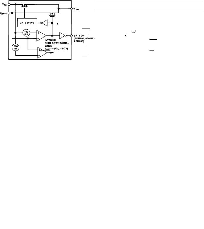
Battery Switchover Section
The battery switchover circuit compares VCC to the VBATT input, and connects VOUT to whichever is higher. Switchover
occurs when VCC is 50 mV higher than VBATT as VCC falls, and when VCC is 70 mV greater than VBATT as VCC rises. This
20 mV of hysteresis prevents repeated rapid switching if VCC falls very slowly or remains nearly equal to the battery voltage.
Figure 1. Battery Switchover Schematic
During normal operation with VCC higher than VBATT, VCC is internally switched to VOUT via an internal PMOS transistor
switch. This switch has a typical on-resistance of 1.5 Ω and can
supply up to 100 mA at the VOUT terminal. VOUT is normally used to drive a RAM memory bank which may require instanta-
neous currents of greater than 100 mA. If this is the case then a bypass capacitor should be connected to VOUT. The capacitor will provide the peak current transients to the RAM. A capacitance value of 0.1 μF or greater may be used.
If the continuous output current requirement at VOUT exceeds 100 mA or if a lower VCC–VOUT voltage differential is desired, an external PNP pass transistor may be connected in parallel with the internal transistor. The BATT ON output (ADM691/ ADM693/ADM695) can directly drive the base of the external transistor.
A 20 Ω MOSFET switch connects the VBATT input to VOUT during battery backup. This MOSFET has very low input-to-
output differential (dropout voltage) at the low current levels required for battery back up of CMOS RAM or other low power CMOS circuitry. The supply current in battery back up is typically 0.6 μA.
The ADM690/ADM691/ADM694/ADM695 operates with battery voltages from 2.0 V to 4.25 V and the ADM692/ADM693 operates with battery voltages from 2.0 V to 4.0 V. High value capacitors, either standard electrolytic or the farad size double layer capacitors, can also be used for short-term memory back up. A small charging current of typically 10 nA (0.1 μA max)
flows out of the VBATT terminal. This current is useful for maintaining rechargeable batteries in a fully charged condition.
This extends the life of the back up battery by compensating for its self discharge current. Also note that this current poses no problem when lithium batteries are used for back up since the maximum charging current (0.1 μA) is safe for even the smallest lithium cells.
If the battery-switchover section is not used, VBATT should be connected to GND and VOUT should be connected to VCC.
REV. A |
–5– |
Loading...