


ADSP-BF522C
Table of contents
 Loading...
ANALOG DEVICES ADSP-BF522C, ADSP-BF523C, ADSP-BF524C, ADSP-BF525C, ADSP-BF526C Service Manual
...
Blackfin and the Blackfin logo are registered trademarks of Analog Devices, Inc.
Blackfin Embedded
Processor with Codec
ADSP-BF522C/ADSP-BF523C/ADSP-BF524C/ADSP-BF525C/ADSP-BF526C/ADSP-BF527C
Rev. A
Information furnished by Analog Devices is believed to be accurate and reliable.
However, no responsibility is assumed by Analog Devices for its use, nor for any
infringements of patents or other rights of third parties that may result from its use.
Specifications subject to change without notice. No license is granted by implication
or otherwise under any patent or patent rights of Analog Devices. Trademarks and
registered trademarks are the property of their respective owners.
One Technology Way, P.O. Box 9106, Norwood, MA 02062-9106 U.S.A.
Tel: 781.329.4700 www.analog.com
Fax: 781.461.3113 © 2010 Analog Devices, Inc. All rights reserved.
PROCESSOR FEATURES
Up to 600 MHz high performance Blackfin processor
RISC-like register and instruction model for ease of
programming and compiler-friendly support
Advanced debug, trace, and performance monitoring
Accepts a wide range of supply voltages for internal and I/O
operations. See operating conditions in the published
ADSP-BF52x processor data sheet.
Programmable on-chip voltage regulator (ADSP-BF523/
ADSP-BF525/ADSP-BF527processors only)
Embedded low power audio codec
289-ball (12 mm x 12 mm) CSP_BGA package
132K bytes of on-chip memory
External memory controller with glueless support for SDRAM
and asynchronous 8-bit and 16-bit memories
Flexible booting options from external flash, SPI and TWI
memory or from host devices including SPI, TWI, and UART
Code security with Lockbox Secure Technology
one-time-programmable (OTP) memory
Memory management unit providing memory protection
2 dual-channel memory DMA controllers
EMBEDDED CODEC FEATURES
Stereo, 24-bit ADCs and DACs
DAC SNR: 100 dB (A-weighted), THD: –80 dB at 48 kHz, 3.3 V
ADC SNR: 90 dB (A-weighted), THD: –80 dB at 48 kHz, 3.3 V
Highly efficient headphone amplifier
Stereo line input and monaural microphone input
Low power
7 mW stereo playback (1.8 V supply)
14 mW record and playback (1.8 V supply)
Low supply voltages
Analog: 1.8 V to 3.6 V
Digital core: 1.8 V min
Digital I/O: 1.8 V to 3.6 V
256 × f
S
/384 × f
S
oversampling rate in normal mode;
250 × f
S
/272 × f
S
oversampling rate in USB mode
Audio sampling rates: 8 kHz, 11.025 kHz, 12 kHz, 16 kHz,
22.05 kHz, 24 kHz, 32 kHz, 44.1 kHz, 48 kHz, 88.2 kHz,
and 96 kHz
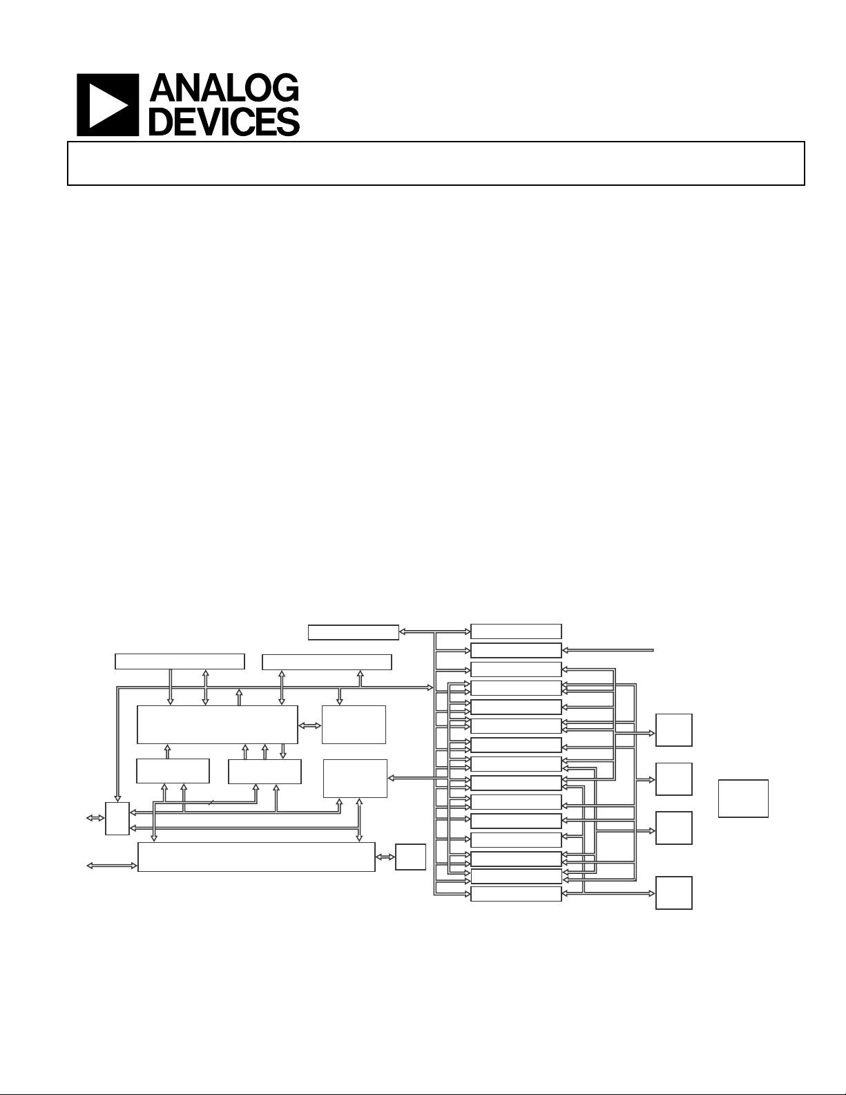
PERIPHERALS
See the published ADSP-BF52x processor data sheet for
additional peripherals
SPORT0
TIMER0
VOLTAGE REGULATOR*
*REGULATOR AVAILABLE ON ADSP-BF523/ADSP-BF525/ADSP-BF527 PROCESSORS ONLY
PORT J
GPIO
PORT H
GPIO
PORT G
GPIO
PORT F
JTAG TEST AND EMULATION
PERIPHERAL
ACCESS BUS
OTP MEMORY
COUNTER
WATCHDOG TIMER
RTC
TWI
SPORT1
NFC
PPI
UART 0
SPI
TIMER7-1
EMAC
HOST DMA
BOOT
ROM
DMA
ACCESS
BUS
INTERRUPT
CONTROLLER
DMA
CONTROLLER
L1 DATA
MEMORY
L1 INSTRUCTION
MEMORY
USB
16
DCB
EAB
EXTERNAL PORT
FLASH, SDRAM CONTROL
B
UART 1
DEB
CODEC

Rev. A | Page 2 of 36 | March 2010
ADSP-BF522C/ADSP-BF523C/ADSP-BF524C/ADSP-BF525C/ADSP-BF526C/ADSP-BF527C
TABLE OF CONTENTS
Processor Features ................................................... 1
Embedded Codec Features ......................................... 1
Peripherals ............................................................. 1
Table of Contents ..................................................... 2
Revision History ...................................................... 2
General Description ................................................. 3
Codec Description ................................................ 3
ADC and DAC ..................................................... 4
ADC High-Pass and DAC De-Emphasis Filters ............ 4
Analog Audio Interfaces ......................................... 4
Stereo Line and Monaural Microphone Inputs .......... 4
Bypass and Sidetone Paths to Output ...................... 5
Line and Headphone Outputs ............................... 5
Digital Audio Interface ........................................... 6
Recording Mode ................................................ 8
Playback Mode .................................................. 8
Digital Audio Data Sampling Rate .......................... 8
Software Control Interface .................................... 11
Codec Pin Descriptions ........................................... 12
Register Details ..................................................... 15
Bit Descriptions .................................................. 16
Specifications ........................................................ 21
Operating Conditions ........................................... 21
Codec Electrical Characteristics .............................. 21
Absolute Maximum Ratings ................................... 23
ESD Sensitivity ................................................... 23
Package Information ............................................ 23
Power Consumption ............................................ 24
Timing Specifications ........................................... 25
TWI Timing ................................................... 25
SPI Timing ..................................................... 26
Digital Audio Interface Slave Mode Timing ............ 27
Digital Audio Interface Master Mode Timing .......... 28
System Clock Timing ........................................ 29
Digital Filter Characteristics ................................ 30
Converter Filter Response ..................................... 30
Digital De-Emphasis ............................................ 31
289-Ball CSP_BGA Ball Assignment ........................ 32
Outline Dimensions ................................................ 35
Ordering Guide ..................................................... 36
REVISION HISTORY
3/10—Rev. 0 to Rev. A
Revised the following figures.
Recommended Application Circuit Using SPI Control ... . 13
Recommended Application Circuit Using TWI Control .. 14
Added Sampling Rate = 48 kHz to all figures in
Converter Filter Response ........................................ 30
Revised Ordering Guide .......................................... 36
ADSP-BF522C/ADSP-BF523C/ADSP-BF524C/ADSP-BF525C/ADSP-BF526C/ADSP-BF527C
Rev. A | Page 3 of 36 | March 2010
GENERAL DESCRIPTION
This document describes the differences between the
ADSP-BF52xC and the ADSP-BF52x standard Blackfin
®
prod-
uct. Please refer to the published ADSP-BF52x data sheet for
general description and specifications. This document only
describes the differences from that data sheet.
The ADSP-BF52xC processors add a low power, high quality
stereo audio codec for portable digital audio applications with
one set of stereo programmable gain amplifier (PGA) line
inputs and one monaural microphone input. It features two 24-
bit analog-to-digital converter (ADC) channels and two 24-bit
digital-to-analog (DAC) converter channels.
The codec can operate as a master or a slave. It supports various
master clock frequencies, including 12 MHz or 24 MHz for USB
devices; standard 256 × f
S
or 384 × f
S
based rates, such as
12.288 MHz and 24.576 MHz; and many common audio sam-
pling rates, such as 96 kHz, 88.2 kHz, 48 kHz, 44.1 kHz, 32 kHz,
24 kHz, 22.05 kHz, 16 kHz, 12 kHz, 11.025 kHz, and 8 kHz.
The codec can operate at power supplies as low as 1.8 V for the
analog circuitry and as low as 1.8 V for the digital circuitry. The
maximum voltage supply is 3.6 V for all supplies.
The codec software-programmable stereo output options
provide the programmer with many application possibilities
because the device can be used as a headphone driver or as a
speaker driver. Its volume control functions provide a large
range of gain control of the audio signal.
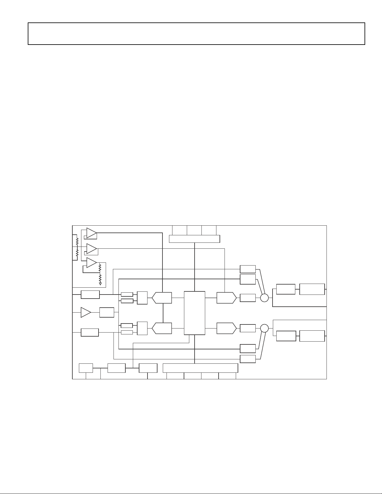
CODEC DESCRIPTION
The ADSP-BF52xC codec contains a central clock source, called
the codec master clock (CODEC_MCLK) that produces a refer-
ence clock for all internal audio data processing and synch-
ronization. When using an external clock source to drive the
CODEC_MCLK pin, care should be taken to select a clock
source with less than 50 ps of jitter. Without careful generation
of the CODEC_MCLK signal, the digital audio quality
will suffer.
To enable the codec to generate the central reference clock
in a system, connect a crystal oscillator between the XTI/
CODEC_MCLK input pin and the XTO output pin.
Figure 1. Codec Block Diagram
CODEC
AVDD
VMID
AGND
MICBIAS
CSB CSDA CSCL CMODE
CONTROL INTERFACE
RLINEIN
MICIN
LLINEIN
OSCPD
OSC
CLKIN
DIVIDER
CLKOUT
DIVIDER
DIGITAL AUDIO INTERFACE
VOLUME
VOLUME
MIC
BOOST
MUTE
MUTE
MUTE
MUTE
MUX
MUX
ADC
ADC
DIGITAL
FILTERS
HPVDD
HPGND
RHPOUT
ROUT
LOUT
LHPOUT
HEADPHONE
DRIVER
HEADPHONE
DRIVER
VOLUME/
MUTE
VOLUME/
MUTE
MUTE
ATTEN/
MUTE
ATTEN/
MUTE
MUTEDAC
DAC MUTE
MUTE
Σ
Σ
XTO
XTI/CODEC_MCLK
CODEC_CLKOUT
DACDAT
DACLRC
CODEC_BCLK
ADCLRC
ADCDAT
Rev. A | Page 4 of 36 | March 2010
ADSP-BF522C/ADSP-BF523C/ADSP-BF524C/ADSP-BF525C/ADSP-BF526C/ADSP-BF527C
To allow an external device to generate the central reference
clock, apply the external clock signal directly through the XTI/
CODEC_MCLK input pin. In this configuration, the oscillator
circuit of the codec can be powered down by using the OSCPD
bit (Register R6, Bit D5) to reduce power consumption.
To accommodate applications with very high frequency master
clocks, the internal core reference clock of the codec can be set
to either CODEC_MCLK or CODEC_MCLK divided by 2. This
is enabled by adjusting the setting of the CLKDIV2 bit (Register
R8, Bit D6). The CODEC_CLKOUT pin can also drive external
clock sources with either the codec clock signal or codec clock
divided by 2 by enabling the CLKODIV2 bit (Register R8,
Bit D7).
ADC AND DAC
The codec contains a pair of oversampling Σ-Δ ADCs. The
maximum ADC full-scale input level is 1.0 V
rms
when
AVDD = 3.3 V. If the input signal to the ADC exceeds this
level, data overloading occurs and causes audible distortion.
The ADC can accept analog audio input from either the stereo
line inputs or the monaural microphone input. Note that the
ADC can only accept input from a single source, so the pro-
grammer must choose either the line inputs or the microphone
input using the INSEL bit (Register R4, Bit D2). The digital data
from the ADC output, once converted, is processed using the
ADC filters.
Complementary to the Σ-Δ ADC channels, the codec contains a
pair of oversampling DACs that convert the digital audio data
from the internal DAC filters into an analog audio signal. The
DAC output can also be muted by setting the DACMU bit (Reg-
ister R5, Bit D3) in the control register.
ADC HIGH-PASS AND DAC DE-EMPHASIS FILTERS
The ADC and DAC employ separate digital filters that perform
24-bit signal processing. The digital filters are used for both
record and playback modes and are optimized for each individ-
ual sampling rate used.
For recording mode operations, the unprocessed data from the
ADC enters the ADC filters and is converted to the appropriate
sampling frequency, then is output to the digital audio interface.
For playback mode operations, the DAC filters convert the digi-
tal audio interface data to oversampled data using a sampling
rate selected by the programmer. The oversampled data is pro-
cessed by the DAC and sent to the analog output mixer by
enabling the DACSEL (Register R4, Bit D4).
Programmers have the option of setting up the device so that
any dc offset in the input source signal is automatically detected
and removed. To accomplish this, enable the digital high-pass
filter (see Table 22 on Page 30 for characteristics) contained in
the ADC digital filters by using the ADCHPD bit (Register R5,
Bit D0).
In addition, programmers can implement digital de-emphasis
by using the DEEMPH bits (Register R5, Bit D1 and Bit D2).
ANALOG AUDIO INTERFACES
The codec includes stereo single-ended line inputs and a mon-
aural microphone input to the on-board ADC. Either the line
inputs or the microphone input, but not both simultaneously,
can be connected to the ADC by setting the INSEL bit (Register
R4, Bit D2).
The codec also includes line and headphone outputs from the
on-board DAC. The line or microphone inputs can be routed
and mixed directly to the output terminals.
Stereo Line and Monaural Microphone Inputs
The single-ended stereo line inputs (RLINEIN and LLINEIN)
are internally biased to VMID by way of a voltage divider
between AVDD and AGND (see Figure 2). The line input signal
can be connected to the internal ADC and, if desired, routed
directly to the outputs via the bypass path by using the BYPASS
bit (Register R4, Bit D3).
The line input volume can be adjusted from –34.5 dB to +33 dB
in steps of +1.5 dB by setting the LINVOL (Register R0, Bit D0
to Bit D5) and RINVOL (Register R1, Bit D0 to Bit D5) bits. By
default the volume is independently adjustable for both right
and left line inputs. However, if the LRINBOTH or RLINBOTH
bit is programmed, both LINVOL and RINVOL are loaded with
the same value. The programmer can also set the LINMUTE
(Register R0, Bit D7) and RINMUTE (Register R1, Bit D7) bits
to mute the line input signal to the ADC.
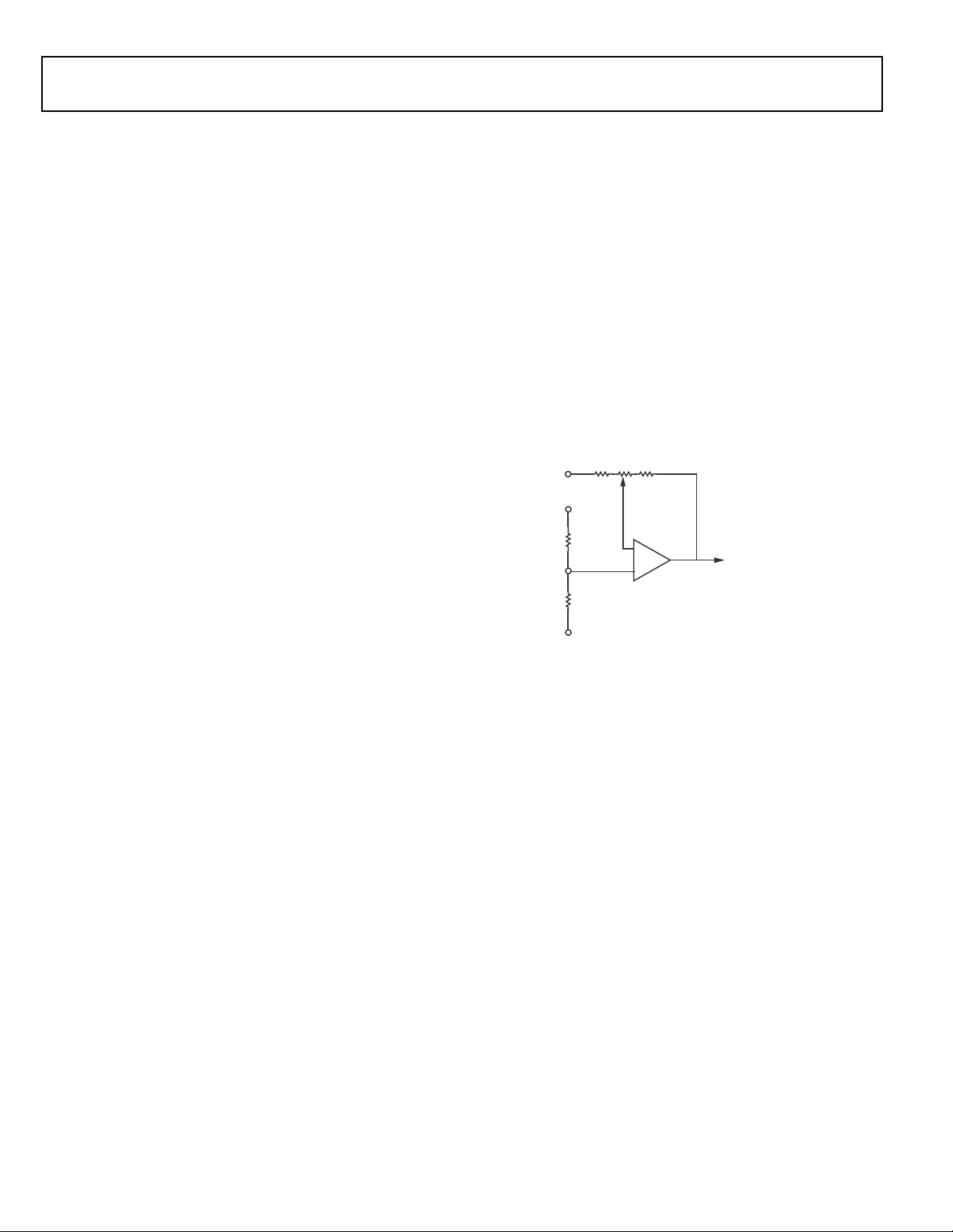
The high impedance, low capacitance monaural microphone
input pin (MICIN, shown in Figure 3 ) has two gain stages and a
microphone bias level (MICBIAS) that is internally biased to the
VMID voltage level by way of a voltage divider between AVDD
and AGND. The microphone input signal can be connected to
the internal ADC and, if desired, routed directly to the outputs
via the sidetone path by using the SIDETONE bit (Register R4,
Bit D5).
Figure 2. Line Input to ADC
ADC
OR
BYPASS
RLINEIN
or
LLINEIN
AVDD
VMID
AGND
+
–
INTERNAL CIRCUITRY

ADSP-BF522C/ADSP-BF523C/ADSP-BF524C/ADSP-BF525C/ADSP-BF526C/ADSP-BF527C
Rev. A | Page 5 of 36 | March 2010
The first gain stage is composed of a low noise operational
amplifier set to an inverting configuration with integrated
50 kΩ feedback and 10 kΩ input resistors. The default micro-
phone input signal gain is 14 dB. An external resistor (R
EXT
) can
be connected in series with the MICIN pin to reduce the first-
stage gain of the microphone input signal to as low as 0 dB by
using the following equation:
Microphone Input Gain = 50 kΩ/(10 kΩ + R
EXT
)
The second-stage gain of the microphone signal path is derived
from the internal microphone boost circuitry. The available set-
tings are 0 dB, 20 dB, and 40 dB and are controlled by the
MICBOOST (Register R4, Bit D0) and MICBOOST2 (Register
R4, Bit D8) bits. To achieve 20 dB of secondary gain boost, the
programmer can select either MICBOOST or MICBOOST2. To
achieve 40 dB of secondary microphone signal gain, the pro-
grammer must select both MICBOOST and MICBOOST2.
The MUTEMIC bit (Register R4, Bit D1) mutes the microphone
input signal to the ADC.
When using either the line or microphone inputs, the maximum
full-scale input to the ADC is 1.0 V rms when AVDD = 3.3 V.
Do not apply an input voltage larger than full-scale to avoid
overloading the ADC, which causes distortion of sound and
deterioration of audio quality. For best sound quality in both
microphone and line inputs, gain should be carefully configured
so that the ADC receives a signal equal to its full-scale. This
maximizes the signal-to-noise ratio for best total audio quality.
Bypass and Sidetone Paths to Output
The line and microphone inputs can be routed and mixed
directly to the output terminals by programming the SIDET-
ONE (Register R4, Bit D5) and BYPASS (Register R4, Bit D3)
registers. In both modes, the analog input signal is routed
directly to the output terminals and is not digitally converted.
The bypass signal at the output mixer is the same level as the
output of the PGA associated with each line input.
The sidetone signal at the output mixer can be attenuated from
–6 dB to –15 dB in steps of –3 dB by configuring the SIDEATT
(Register R4, Bit D6 and Bit D7) control register bits. The
selected level of attenuation occurs after the initial microphone
signal amplification from the microphone first and second stage
gains.
Line and Headphone Outputs
The DAC outputs, the microphone (the sidetone path), and the
line inputs (the bypass path) are summed at an output mixer
(see Figure 4). This output signal is then applied to both the ste-
reo line outputs and stereo headphone outputs.
The codec has a set of efficient headphone amplifier outputs,
LHPOUT and RHPOUT, that are able to drive 16 Ω or 32 Ω
headphones (shown in Figure 5).
Like the line inputs, the LHPOUT and RHPOUT volumes, by
default, are independently adjusted by setting the LHPVOL
(Register R2, Bit D0 to Bit D6) and RHPVOL (Register R3, Bit
D0 to Bit D6) bits of the headphone output control registers.
The headphone outputs can be muted by writing codes less than
0110000 to the LHPVOL and RHPVOL bits.
Figure 3. Microphone Input to ADC
ADC
OR
SIDETONE
INTERNAL CIRCUITRY
MICIN
AVDD
VMID
AGND
R
EXT
10kΩ
50kΩ
0dB/20dB/40dB
GAIN BOOST
Figure 4. Output Signal Chain
Figure 5. Headphone Output
LINE OUTPUT
AND
HEADPHONE
OUTPUT
AVDD
VMID
AGND
BYPASS
SIDETONE
DACSEL
LINE
INPUT
MICROPHONE
INPUT
DAC
OUTPUT
INTERNAL CIRCUITRY
RHPOUT
or
LHPOUT
DAC/
SIDETONE/
BYPASS
AVDD
VMID
AGND
+
–
INTERNAL CIRCUITRY
Rev. A | Page 6 of 36 | March 2010
ADSP-BF522C/ADSP-BF523C/ADSP-BF524C/ADSP-BF525C/ADSP-BF526C/ADSP-BF527C
The programmer can simultaneously load the volume control of
both channels by writing to the LRHPBOTH (Register R2, Bit
D8) and RLHPBOTH (Register R3, Bit D8) bits of the left- or
right-channel DAC volume registers.
The maximum output level of the headphone outputs is
1.0 V rms when AVDD and HPVDD = 3.3 V. To suppress audi-
ble pops and clicks, the headphone and line outputs are held at
the VMID dc voltage level when the device is set to standby
mode or when the headphone outputs are muted.
The stereo line outputs of the codec, the LOUT and ROUT pins,
can drive a load impedance of 10 kΩ and 50 pF. The line output
signal levels are not adjustable at the output mixer, which has a
fixed gain of 0 dB. The maximum output level of the line out-
puts is 1.0 V rms when AVDD = 3.3 V.
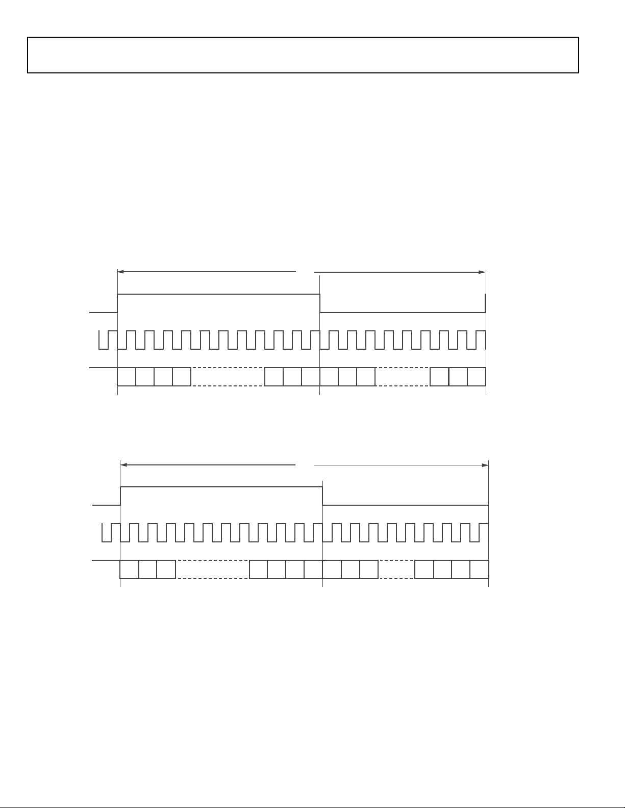
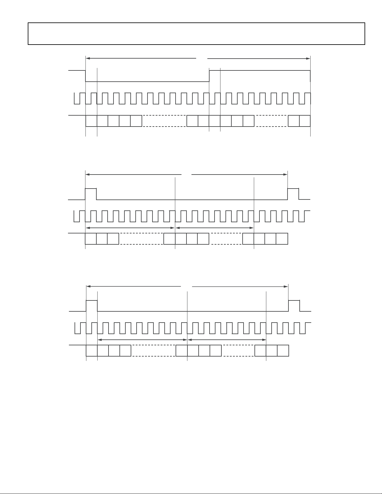
DIGITAL AUDIO INTERFACE
The digital audio input can support the following digital audio
communication protocols: right-justified mode, left-justified
mode, I
2
S mode, and frame sync mode. See Figure 6 on Page 6
through Figure 10 on Page 7.
The mode selection is performed by writing to the FORMAT
bits of the digital audio interface register (Register R7, Bit D1
and Bit D0). All modes are MSB first and operate with data of 16
to 32 bits.
Figure 6. Left-Justified Audio Input Mode
Figure 7. Right-Justified Audio Input Mode
ADCLRC/
DACLRC
CODEC_BCLK
ADCDAT/
DACDAT
1234 NXX XXN12
LEFT CHANNEL
3
RIGHT CHANNEL
1/
f
S
X = DON’T CARE.
ADCLRC/
DACLRC
CODEC_BCLK
ADCDAT/
DACDAT
LEFT CHANNEL RIGHT CHANNEL
1/
f
S
X = DON’T CARE.
XNX
32 1 XXN4 4321
ADSP-BF522C/ADSP-BF523C/ADSP-BF524C/ADSP-BF525C/ADSP-BF526C/ADSP-BF527C
Rev. A | Page 7 of 36 | March 2010
Figure 8. I
2
S Audio Input Mode
Figure 9. Frame Sync/PCM Mode Audio Input (Submode 1) [Bit LRP = 0]
Figure 10. Frame Sync/PCM Mode Audio Input (Submode 2) [Bit LRP = 1]
ADCLRC/
DACLRC
CODEC_BCLK
ADCDAT/
DACDAT
1234X XN
LEFT CHANNEL RIGHT CHANNEL
1/
f
S
X = DON’T CARE.
NX123X
ADCLRC/
DACLRC
CODEC_BCLK
ADCDAT/
DACDAT
LEFT CHANNEL RIGHT CHANNEL
1/
f
S
X = DON’T CARE.
231
123N
XXXN
ADCLRC/
DACLRC
CODEC_BCLK
ADCDAT/
DACDAT
LEFT CHANNEL RIGHT CHANNEL
1/
f
S
X = DON’T CARE.
231X
123N
XXN

Rev. A | Page 8 of 36 | March 2010
ADSP-BF522C/ADSP-BF523C/ADSP-BF524C/ADSP-BF525C/ADSP-BF526C/ADSP-BF527C
Recording Mode
The digital audio interface sends the ADC digital filter data to
the ADCDAT output pin for recording. The ADCDAT data
stream multiplexes the left- and right-channel audio data in the
time domain. The ADCLRC clock signal separates left- and
right-channel digital audio frames on the ADCDAT lines.
The CODEC_BCLK signal clocks the digital audio data within
the frames. The CODEC_BCLK signal is either an input or an
output depending on whether the codec is in master or slave
mode. During a recording operation, ADCDAT and ADCLRC
must be synchronous to the CODEC_BCLK signal to avoid data
corruption.
Playback Mode
The digital audio interface receives data on the DACDAT input
pin for playback. The digital audio data stream on the DACDAT
pin is time-domain-multiplexed left and right channel audio
data. The DACLRC clock signal separates left and right channel
digital audio frames on the DACDAT lines.
The CODEC_BCLK signal clocks the digital audio data within
the frames. The CODEC_BCLK signal is either an input or an
output depending on whether the codec is in master or slave
mode. During a playback operation, DACDAT and DACLRC
must be synchronous to the CODEC_BCLK signal to avoid data
corruption.
Digital Audio Data Sampling Rate
To accommodate a wide variety of commonly used DAC and
ADC sampling rates, the codec allows for two modes of opera-
tion, normal and USB, selected by the USB bit (Register R8,
Bit D0).
The sampling rate is generated as a fixed divider from the
CODEC_MCLK signal. Because all audio processing references
the CODEC_MCLK signal, corruption of this signal w ill cor rupt
the quality of the audio at the codec output. The ADCLRC/
ADCDAT/CODEC_BCLK or DACLRC/DACDAT/
CODEC_BCLK signals must be synchronized with
CODEC_MCLK in the digital audio interface circuit.
CODEC_MCLK must be faster or equal to the CODEC_BCLK
frequency to guarantee that no data is lost during data synchro-
nization. The CODEC_BCLK frequency should be greater than
the sampling rate × word length × 2. Ensuring that the
CODEC_BCLK frequency is greater than this, guarantees that
all valid data bits are captured by the digital audio interface cir-
cuitry. For example, if a 32 kHz digital audio sampling rate with
a 32-bit word length is desired, CODEC_BCLK = 2.048 MHz.
ADSP-BF522C/ADSP-BF523C/ADSP-BF524C/ADSP-BF525C/ADSP-BF526C/ADSP-BF527C
Rev. A | Page 9 of 36 | March 2010
Normal Mode
In normal mode, the codec supports digital audio sampling
rates from 8 kHz to 96 kHz. Normal mode supports 256 × f
S
and
384 × f
S
based clocks. To select the desired sampling rate, the
programmer must set the appropriate sampling rate register in
the SR control bits (Register R8, Bit D2 to Bit D5) and match
this selection to the core clock frequency that is pulsed on the
CODEC_MCLK pin. See Table 1 for sampling rates in
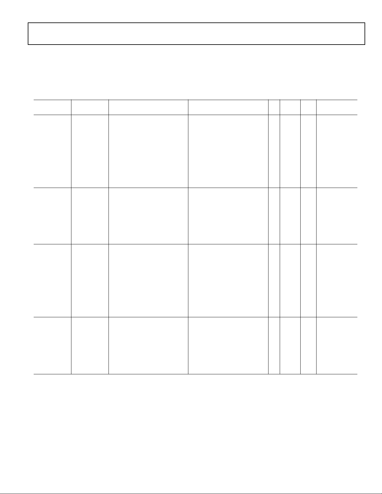
normal mode.
Table 1. Sampling Rate Lookup Table, Normal Mode (USB Disabled)
CODEC_MCLK
(CLKDIV2 = 0)
CODEC_MCLK
(CLKDIV2 = 1)
ADC Sampling Rate
(ADCLRC)
DAC Sampling Rate
(DACLRC)
USB SR [3:0] BOSR CODEC_BCLK
(MS = 1)
1
12.288 MHz 24.576 MHz 8 kHz (CODEC_MCLK/1536) 8 kHz (CODEC_MCLK/1536) 0 0011 0 CODEC_MCLK/4
8 kHz (CODEC_MCLK/1536) 48 kHz (CODEC_MCLK/256) 0 0010 0 CODEC_MCLK/4
12 kHz (CODEC_MCLK/1024) 12 kHz (CODEC_MCLK/1024) 0 0100 0 CODEC_MCLK/4
16 kHz (CODEC_MCLK/768) 16 kHz (CODEC_MCLK/768) 0 0101 0 CODEC_MCLK/4
24 kHz (CODEC_MCLK/512) 24 kHz (CODEC_MCLK/512) 0 1110 0 CODEC_MCLK/4
32 kHz (CODEC_MCLK/384) 32 kHz (CODEC_MCLK/384) 0 0110 0 CODEC_MCLK/4
48 kHz (CODEC_MCLK/256) 8 kHz (CODEC_MCLK/1536) 0 0001 0 CODEC_MCLK/4
48 kHz (CODEC_MCLK/256) 48 kHz (CODEC_MCLK/256) 0 0000 0 CODEC_MCLK/4
96 kHz (CODEC_MCLK/128) 96 kHz (CODEC_MCLK/128) 0 0111 0 CODEC_MCLK/2
11.2896 MHz 22.5792 MHz 8.0182 kHz (CODEC_MCLK/1408) 8.0182 kHz (CODEC_MCLK/1408) 0 1011 0 CODEC_MCLK/4
8.0182 kHz (CODEC_MCLK/1408) 44.1 kHz (CODEC_MCLK/256) 0 1010 0 CODEC_MCLK/4
11.025 kHz (CODEC_MCLK/1024) 11.025 kHz (CODEC_MCLK/1024) 0 1100 0 CODEC_MCLK/4
22.05 kHz (CODEC_MCLK/512) 22.05 kHz (CODEC_MCLK/512) 0 1101 0 CODEC_MCLK/4
44.1 kHz (CODEC_MCLK/256) 8.0182 kHz (CODEC_MCLK/1408) 0 1001 0 CODEC_MCLK/4
44.1 kHz (CODEC_MCLK/256) 44.1 kHz (CODEC_MCLK/256) 0 1000 0 CODEC_MCLK/4
88.2 kHz (CODEC_MCLK/128) 88.2 kHz (CODEC_MCLK/128) 0 1111 0 CODEC_MCLK/2
18.432 MHz 36.864 MHz 8 kHz (CODEC_MCLK/2304) 8 kHz (CODEC_MCLK/2304) 0 0011 1 CODEC_MCLK/6
8 kHz (CODEC_MCLK/2304) 48 kHz (CODEC_MCLK/384) 0 0010 1 CODEC_MCLK/6
12 kHz (CODEC_MCLK/1536) 12 kHz (CODEC_MCLK/1536) 0 0100 1 CODEC_MCLK/6
16 kHz (CODEC_MCLK/1152) 16 kHz (CODEC_MCLK/1152) 0 0101 1 CODEC_MCLK/6
24 kHz (CODEC_MCLK/768) 24 kHz (CODEC_MCLK/768) 0 1110 1 CODEC_MCLK/6
32 kHz (CODEC_MCLK/576) 32 kHz (CODEC_MCLK/576) 0 0110 1 CODEC_MCLK/6
48 kHz (CODEC_MCLK/384) 48 kHz (CODEC_MCLK/384) 0 0000 1 CODEC_MCLK/6
48 kHz (CODEC_MCLK/384) 8 kHz (CODEC_MCLK/2304) 0 0001 1 CODEC_MCLK/6
96 kHz (CODEC_MCLK/192) 96 kHz (CODEC_MCLK/192) 0 0111 1 CODEC_MCLK/3
16.9344 MHz 33.8688 MHz 8.0182 kHz (CODEC_MCLK/2112) 8.0182 kHz (CODEC_MCLK/2112) 0 1011 1 CODEC_MCLK/6
8.0182 kHz (CODEC_MCLK/2112) 44.1 kHz (CODEC_MCLK/384) 0 1010 1 CODEC_MCLK/6
11.025 kHz (CODEC_MCLK/1536) 11.025 kHz (CODEC_MCLK/1536) 0 1100 1 CODEC_MCLK/6
22.05 kHz (CODEC_MCLK/768) 22.05 kHz (CODEC_MCLK/768) 0 1101 1 CODEC_MCLK/6
44.1 kHz (CODEC_MCLK/384) 8.0182 kHz (CODEC_MCLK/2112) 0 1001 1 CODEC_MCLK/6
44.1 kHz (CODEC_MCLK/384) 44.1 kHz (CODEC_MCLK/384) 0 1000 1 CODEC_MCLK/6
88.2 kHz (CODEC_MCLK/192) 88.2 kHz (CODEC_MCLK/192) 0 1111 1 CODEC_MCLK/3
1
CODEC_BCLK frequency is for master mode and slave right-justified mode only.

Rev. A | Page 10 of 36 | March 2010
ADSP-BF522C/ADSP-BF523C/ADSP-BF524C/ADSP-BF525C/ADSP-BF526C/ADSP-BF527C
USB Mode
In USB mode, the codec supports digital audio sampling rates
from 8 kHz to 96 kHz. USB mode is enabled on the codec
to support the common universal serial bus (USB) clock rate of
12 MHz, or to support 24 MHz if the CLKDIV2 control register
bit is activated. The programmer must set the appropriate sam-
pling rate in the SR control bits (Register R8, Bit D2 to Bit D5).
See Table 2 for sampling rates in USB mode.
Table 2. Sampling Rate Lookup Table, USB Mode (USB Enabled)
CODEC_MCLK
(CLKDIV2 = 0)
CODEC_MCLK
(CLKDIV2 = 1)
ADC Sampling Rate
(ADCLRC)
DAC Sampling Rate
(DACLRC)
USB SR [3:0] BOSR CODEC_BCLK
(MS = 1)
1
12.000 MHz 24.000 MHz 8 kHz (CODEC_MCLK/1500) 8 kHz (CODEC_MCLK/1500) 1 0011 0 CODEC_MCLK
8 kHz (CODEC_MCLK/1500) 48 kHz (CODEC_MCLK/250) 1 0010 0 CODEC_MCLK
8.0214 kHz (CODEC_MCLK/1496) 8.0214 kHz (CODEC_MCLK/1496) 1 1011 1 CODEC_MCLK
8.0214 kHz (CODEC_MCLK/1496) 44.118 kHz (CODEC_MCLK/272) 1 1010 1 CODEC_MCLK
11.0259 kHz (CODEC_MCLK/1088) 11.0259 kHz (CODEC_MCLK/1088) 1 1100 1 CODEC_MCLK
12 kHz (CODEC_MCLK/1000) 12 kHz (CODEC_MCLK/1000) 1 1000 0 CODEC_MCLK
16 kHz (CODEC_MCLK/750) 16 kHz (CODEC_MCLK/750) 1 1010 0 CODEC_MCLK
22.0588 kHz (CODEC_MCLK/544) 22.0588 kHz (CODEC_MCLK/544) 1 1101 1 CODEC_MCLK
24 kHz (CODEC_MCLK/500) 24 kHz (CODEC_MCLK/500) 1 1110 0 CODEC_MCLK
32 kHz (CODEC_MCLK/375) 32 kHz (CODEC_MCLK/375) 1 0110 0 CODEC_MCLK
44.118 kHz (CODEC_MCLK/272) 8.0214 kHz (CODEC_MCLK/1496) 1 1001 1 CODEC_MCLK
44.118 kHz (CODEC_MCLK/272) 44.118 kHz (CODEC_MCLK/272) 1 1000 1 CODEC_MCLK
48 kHz (CODEC_MCLK/250) 8 kHz (CODEC_MCLK/1500) 1 0001 0 CODEC_MCLK
48 kHz (CODEC_MCLK/250) 48 kHz (CODEC_MCLK/250) 1 0000 0 CODEC_MCLK
88.235 kHz (CODEC_MCLK/136) 88.235 kHz (CODEC_MCLK/136) 1 1111 1 CODEC_MCLK
96 kHz (CODEC_MCLK/125) 96 kHz (CODEC_MCLK/125) 1 0111 0 CODEC_MCLK
1
CODEC_BCLK frequency is for master mode and slave right-justified mode only.
ADSP-BF522C/ADSP-BF523C/ADSP-BF524C/ADSP-BF525C/ADSP-BF526C/ADSP-BF527C
Rev. A | Page 11 of 36 | March 2010
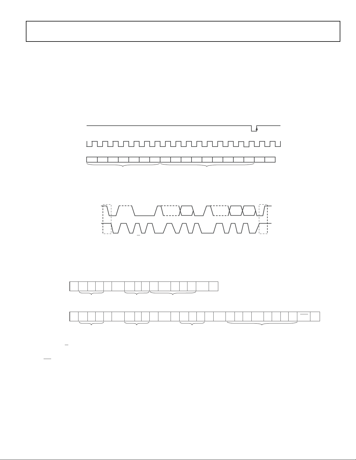
SOFTWARE CONTROL INTERFACE
The software control interface provides access to the
programmer-selectable control registers and can operate with a
2-wire (TWI) or 3-wire (SPI) interface, depending on the setting
of the CMODE pin. If the CMODE pin is set to 0, the 2-wire
interface is selected; if 1, the 3-wire interface is selected.
Within each control register is a control data-word consisting of
16 bits, MSB first. Bit B15 to Bit B9 are the register map address,
and Bit B8 to Bit B0 are register data for the associated register
map.
When 2-wire (TWI) mode is selected, CSDA generates the serial
control data-word; CSCL clocks the serial data; and CSB deter-
mines the TWI device address. If the CSB pin is set to 0, the
address selected is 0011010; if 1, the address is 0011011.
When 3-wire (SPI) mode is selected, CSDA generates the con-
trol data-word, CSCL clocks the control data-word into the
codec, and CSB latches in the control data-word.
Figure 11. Codec SPI Serial Interface
Figure 12. Codec TWI Serial Interface
B15
B14
CSB
CSCL
CSDA
B0B01B02B03B04B05B06B07B08B09B10B11B12B13
REGISTER MAP
ADDRESS
REGISTER
DATA
P981 – 7981 – 7981 – 7
S
CSDA
CSCL
START ADDR R/W ACK ACKSUBADDRESS ACK STOP
DATA
Figure 13. Codec TWI Write and Read Sequences
WRITE
SEQUENCE
READ
SEQUENCE
SA1A7 A0 A(S) A(S) SB15 B9 0
01
0P
0... A1A7 A0 A(S)... B0 B8B7 A(M) A(M)...
B0B7 P...
......
DEVICE
ADDRESS
DEVICE
ADDRESS
REGISTER
ADDRESS
SA1A7 A0 A(S) A(S) A(S)B15 B9 B8
0
... ...
DEVICE
ADDRESS
REGISTER
ADDRESS
REGISTER
DATA
(SLAVE DRIVE)
REGISTER
DATA
S/P = START/STOP BIT.
A0 = I
2
C R/W BIT.
A(S) = ACKNOWLEDGE BY SLAVE.
A(M) = ACKNOWLEDGE BY MASTER.
A(M) = ACKNOWLEDGE BY MASTER (INVERSION).
Loading...