


AD7152
Table of contents
 Loading...
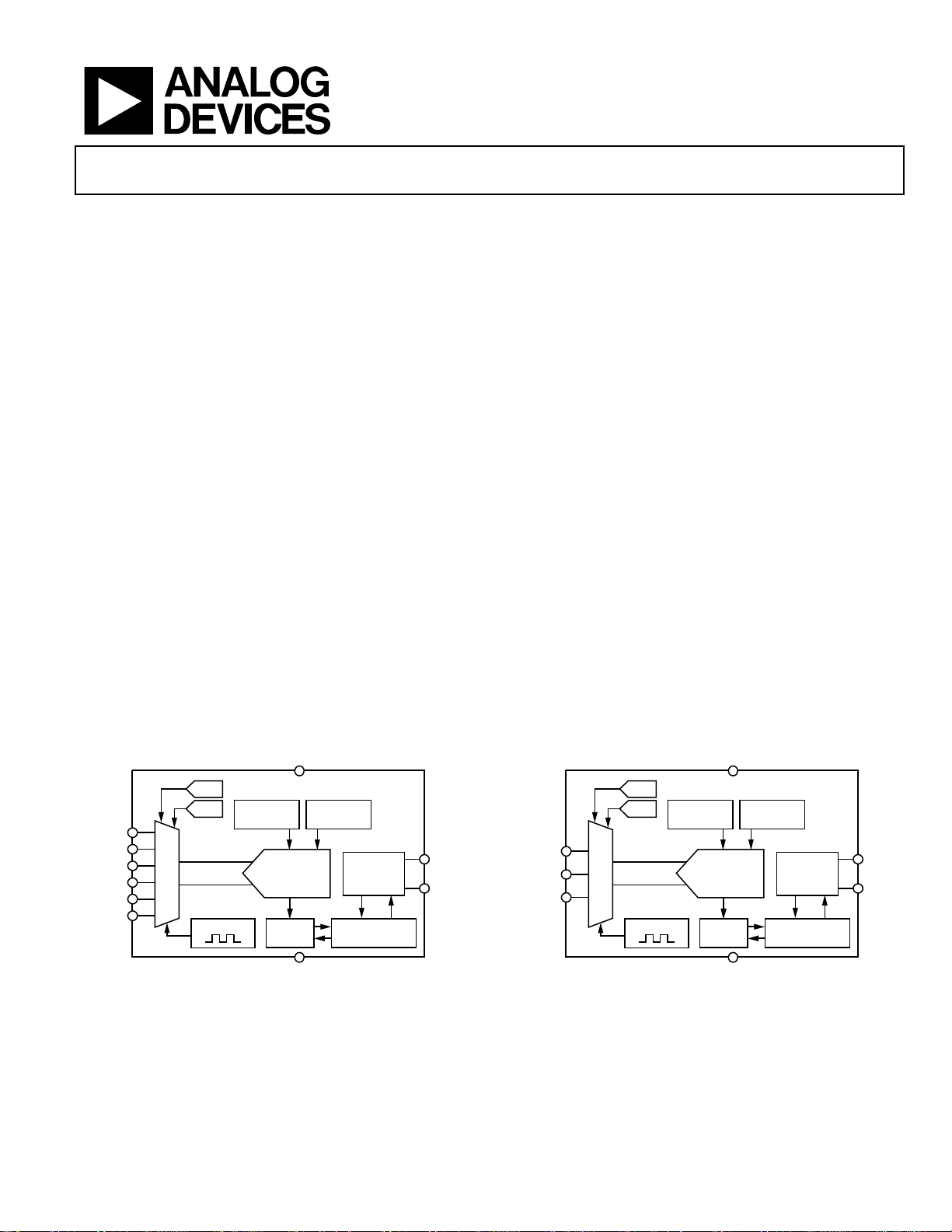
12-Bit Capacitance-to-Digital Converter
AD7152/AD7153
Rev. 0
Information furnished by Analog Devices is believed to be accurate and reliable. However, no
responsibility is assumed by Anal og Devices for its use, nor for any infringements of p atents or other
rights of third parties that may result from its use. Specifications subject to change without notice. No
license is granted by implication or otherwise under any patent or patent rights of Analog Devices.
Trademarks and registered trademarks are the property of their respective owners.
One Technology Way, P.O. Box 9106, Norwood, MA 02062-9106, U.S.A.
Tel: 781.329.4700 www.analog.com
Fax: 781.461.3113 ©2008 Analog Devices, Inc. All rights reserved.
FEATURES
Capacitance-to-digital converters
Interfaces to floating sensors
Resolution down to 0.25 fF (that is, up to 12 ENOB)
Linearity: 0.05%
Common-mode (not changing) capacitance up to 5 pF
Four capacitance ranges selectable per operation mode
±0.25 pF to ±2 pF in differential mode
0.5 pF to 4 pF in single-ended mode
Tolerant of parasitic capacitance to ground up to 50 pF
Conversion time per channel: 5 ms, 20 ms, 50 ms, and 60 ms
Internal clock oscillator
2-wire serial interface (I
2
C-compatible)
Power
2.7 V to 3.6 V single-supply operation
100 μA current consumption
Operating temperature: −40°C to +85°C
10-lead MSOP package
APPLICATIONS
Automotive, industrial, and medical systems for
Pressure measurement
Position sensing
Level sensing
Flowmeters
Humidity sensing
GENERAL DESCRIPTION
The AD7152/AD7153 are 12-bit sigma-delta (Σ-Δ) capacitance-to-
digital converters (CDCs). The capacitance to be measured
is connected directly to the device inputs. The architecture
features inherent high resolution (12-bit no missing codes,
up to 12-bit effective resolution) and high linearity (±0.05%).
The AD7152/AD7153 have four capacitance input ranges per
operation mode, ±0.25 pF to ±2 pF in differential mode and
0.5 pF to 4 pF in single-ended mode.
The AD7152/AD7153 can accept up to 5 pF common-mode
capacitance (not changing), which can be balanced by a
programmable on-chip, digital-to-capacitance converter
(CAPDAC).
The AD7153 has one capacitance input channel, while the
AD7152 has two channels. Each channel can be configured
as single-ended or differential. The AD7152/AD7153 are
designed for floating capacitive sensors.
The AD7152/AD7153 have a 2-wire, I
2
C®-compatible serial
interface. Both parts can operate with a single power supply
from 2.7 V to 3.6 V. They are specified over the temperature
range of −40°C to +85°C and are available in a 10-lead MSOP
package.
FUNCTIONAL BLOCK DIAGRAMS
DIGITAL
FILTER
12-BIT Σ-Δ
MODULATOR
CLOCK
GENERATOR
VOLTAGE
REFERENCE
AD7152
I
2
C
SERIAL
INTERFACE
07450-001
EXCITATI ON
EXC2
CIN1(+)
CIN1(–)
CIN2(+)
CIN2(–)
EXC1
SDA
SCL
V
DD
GND
CONTROL LOGIC
CALIBRATION
CAP+
CAP–
MUX
Figure 1.
DIGITAL
FILTER
12-BIT Σ-Δ
MODULATOR
CLOCK
GENERATOR
VOLTAGE
REFERENCE
AD7153
I
2
C
SERIAL
INTERFACE
07450-002
EXCITATI ON
CIN1(+)
CIN1(–)
EXC1
SDA
SCL
V
DD
GND
CONTROL LOGIC
CALIBRATION
CAP+
CAP–
MUX
Figure 2.

AD7152/AD7153
Rev. 0 | Page 2 of 24
TABLE OF CONTENTS
Features .............................................................................................. 1
Applications ....................................................................................... 1
General Description ......................................................................... 1
Functional Block Diagrams ............................................................. 1
Revision History ............................................................................... 2
Specifications ..................................................................................... 3
Timing Specifications .................................................................. 5
Absolute Maximum Ratings ............................................................ 6
ESD Caution .................................................................................. 6
Pin Configurations and Function Descriptions ........................... 7
Typical Performance Characteristics ............................................. 8
Serial Interface ................................................................................ 11
Write Operation .......................................................................... 11
Read Operation ........................................................................... 11
AD7152/AD7153 Reset ............................................................. 12
General Call................................................................................. 12
Register Map .................................................................................... 13
Status Register ............................................................................. 14
Data Registers ............................................................................. 15
Offset Calibration Registers ...................................................... 15
Gain Calibration Registers ........................................................ 15
CAP Setup Registers .................................................................. 16
Configuration Register .............................................................. 16
CAPDAC POS Register ............................................................. 17
CAPDAC NEG Register ............................................................ 17
Configuration2 Register ............................................................ 17
Circuit Description......................................................................... 18
Capacitance-to-Digital Converter (CDC) .............................. 18
Excitation Source ........................................................................ 18
CAPDAC ..................................................................................... 19
Single-Ended Capacitive Input ................................................. 19
Differential Capacitive Input .................................................... 20
Parasitic Capacitance to Ground .............................................. 20
Parasitic Resistance to Ground ................................................. 20
Parasitic Parallel Resistance ...................................................... 21
Parasitic Serial Resistance ......................................................... 21
Input EMC Protection ............................................................... 21
Power Supply Decoupling and Filtering .................................. 21
Capacitive Gain Calibration ..................................................... 21
Capacitive System Offset Calibration ...................................... 21
Typical Application Diagram .................................................... 22
Outline Dimensions ....................................................................... 23
Ordering Guide .......................................................................... 23
REVISION HISTORY
5/08—Revision 0: Initial Version
AD7152/AD7153
Rev. 0 | Page 3 of 24
SPECIFICATIONS
V
DD
= 2.7 V to 3.6 V; GND = 0 V; −40°C to +85°C, unless otherwise noted.
Table 1.
Parameter Min Typ Max Unit
1
Test Conditions/Comments
CAPACITIVE INPUT
Capacitive Input Ranges ±2 pF Differential mode
±1 pF
±0.5 pF
±0.25 pF
4 pF Single-ended mode
2 pF
1 pF
0.5 pF
Gain Matching Between Ranges ±3 % of FS
Integral Nonlinearity (INL)
2
±0.05 % of FS
No Missing Codes
2
12 Bits
Resolution, p-p
2, 3
10 Bits 25°C, V
DD
= 3.3 V, 4 pF range
Resolution Effective
2, 3
12 Bits 25°C, V
DD
= 3.3 V, 4 pF range
Absolute Error
4
±20 fF
25°C, V
DD
= 3.3 V, after system offset
calibration, ±2 pF range
System Offset Calibration Range
5, 6
40 % of FSR
Offset Deviation over Temperature
2
1 5 fF
Single-ended mode, CIN and EXC
pins disconnected, see Figure 8
0.3 1 fF
Differential mode, CIN and EXC
pins disconnected
Gain Error
7
0.5 % of FSR 25°C, V
DD
= 3.3 V
Gain Deviation over Temperature
2
0.3 0.4 % of FSR See Figure 7
Allowed Capacitance, CIN to GND
2
50 pF See Figure 9 and Figure 10
Allowed Resistance, CIN to GND
2
10 MΩ See Figure 13
Allowed Serial Resistance
2
20 kΩ See Figure 16
Power Supply Rejection DC 2 fF/V See Figure 17
Normal-Mode Rejection
2
−70 dB 50 Hz ± 1 Hz, conversion time = 60 ms
−70 dB 60 Hz ± 1 Hz, conversion time = 50 ms
Channel-to-Channel Isolation
2
−70 dB AD7152 only
CAPDAC
Full Range 5 6.25 pF
Resolution
8
200 fF 5-bit CAPDAC
Differential Nonlinearity (DNL)
2
0.25 LSB See Figure 18 and Figure 19
Offset Deviation over Temperature
2
0.3 % of CAPDAC FSR Single-ended mode
EXCITATION
Frequency 30.9 32 32.8 kHz
Voltage ±V
DD
/2 V
Allowed Capacitance, EXC to GND
2
300 pF See Figure 11 and Figure 12
SERIAL INTERFACE LOGIC INPUTS (SCL, SDA)
Input High Voltage, V
IH
1.5 V
Input Low Voltage, V
IL
0.8 V
Input Leakage Current (SCL) ±0.1 ±5 μA
OPEN-DRAIN OUTPUT (SDA)
Output Low Voltage, V
OL
0.4 V
I
SINK
= −6.0 mA
Output High Leakage Current, I
OH
0.1 5 μA V
OUT
= V
DD
POWER SUPPLY MONITOR
Threshold Voltage, V
DD
2.45 2.65 V

AD7152/AD7153
Rev. 0 | Page 4 of 24
Parameter Min Typ Max Unit
1
Test Conditions/Comments
POWER REQUIREMENTS
V
DD
-to-GND Voltage 2.7 3.6 V V
DD
= 3.3 V, nominal
Current, I
DD
9
100 120 μA
Current Power-Down Mode, I
DD
9
1 5 μA Temperature ≤ 25°C
3 10 μA Temperature = 85°C
1
Capacitance units: 1 pF = 10
−12
F; 1 fF = 10
−15
F; 1 aF = 10
−18
F.
2
Specification is not production tested but is supported by characterization data at initial product release.
3
Except Channel 2 in differential mode. To achieve the specified performance in differential mode, the I
2
C interface must be idle during the capacitance conversion to
prevent signal coupling from the SCL pin to the adjacent CIN2(−) pin.
4
Factory calibrated. The absolute error includes factory gain calibration error and integral nonlinearity error all at 25°C. At different temperatures, compensation for
gain drift over temperature is required.
5
Specification is not production tested but guaranteed by design.
6
A system offset calibration is effectively a conversion; therefore, the offset error is of the order of the conversion noise. This applies after calibration at the temperature,
capacitive input range, and applied V
DD
of interest. The capacitive input offset can be reduced using a system offset calibration. Large offsets should be removed using
CAPDACs.
7
The gain error is factory calibrated at 25°C. At different temperatures, compensation for gain drift over temperature is required.
8
The CAPDAC resolution is five bits in the actual CAPDAC full range. Using the on-chip offset calibration or adjusting the capacitive offset calibration register can
further reduce the CIN offset or the unchanging CIN component.
9
Digital inputs equal to V
DD
or GND.
AD7152/AD7153
Rev. 0 | Page 5 of 24
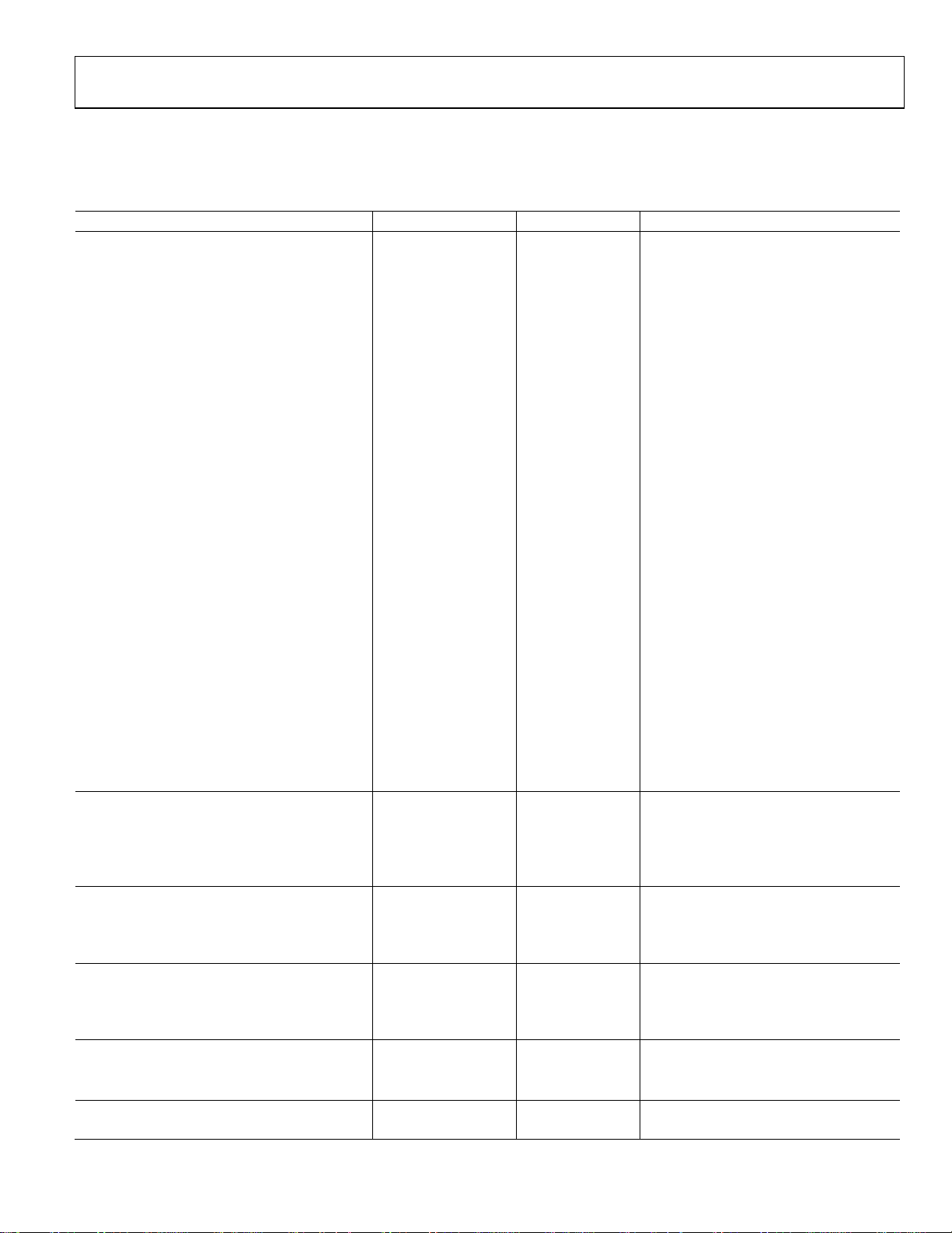
TIMING SPECIFICATIONS
V
DD
= 2.7 V to 3.6 V; GND = 0 V; Input Logic 0 = 0 V; Input Logic 1 = V
DD
; −40°C to +85°C, unless otherwise noted.
Table 2.
Parameter Min Typ Max Unit Test Conditions/Comments
SERIAL INTERFACE
1, 2
See Figure 3.
SCL Frequency 0 400 kHz
SCL High Pulse Width, t
HIGH
0.6 μs
SCL Low Pulse Width, t
LOW
1.3 μs
SCL, SDA Rise Time, t
R
0.3 μs
SCL, SDA Fall Time, t
F
0.3 μs
Hold Time (Start Condition), t
HD;STA
0.6 μs After this period, the first clock is generated.
Set-Up Time (Start Condition), t
SU;STA
0.6 μs Relevant for repeated start condition.
Data Set-Up Time, t
SU;DAT
0.1 μs
Setup Time (Stop Condition), t
SU;STO
0.6 μs
Data Hold Time, t
HD;DAT
(Master) 0.01 μs
Bus-Free Time (Between Stop and Start Conditions, t
BUF
) 1.3 μs
1
Sample tested during initial release to ensure compliance.
2
All input signals are specified with input rise/fall times = 3 ns, measured between the 10% and 90% points. Timing reference points at 50% for inputs and outputs;
output load = 10 pF.
P
S
t
LOW
t
R
t
F
t
HD;STA
t
HD;DAT
t
SU;DAT
t
SU;STA
t
HD;STA
t
SU;STO
t
HIGH
SCL
PS
SDA
t
BUF
07450-003
Figure 3. Serial Interface Timing Diagram
AD7152/AD7153
Rev. 0 | Page 6 of 24
ABSOLUTE MAXIMUM RATINGS
T
A
= 25°C, unless otherwise noted.
Table 3.
Parameter Rating
Positive Supply Voltage, V
DD
to GND −0.3 V to +3.9 V
Voltage on Any Input or Output Pin to GND −0.3 V to V
DD
+ 0.3 V
ESD Rating (ESD Association Human
Body Model, S5.1)
4 kV
ESD Rating (Field-Induced Charged
Device Model)
750 V
Operating Temperature Range −40°C to +85°C
Storage Temperature Range −65°C to +150°C
Junction Temperature 150°C
MSOP
θ
JA
Thermal Impedance-to-Air 206°C/W
θ
JC
Thermal Impedance-to-Case 44°C/W
Reflow Soldering (Pb-Free)
Peak Temperature 260 (+0/−5)°C
Time at Peak Temperature 10 sec to 40 sec
Stresses above those listed under Absolute Maximum Ratings
may cause permanent damage to the device. This is a stress
rating only; functional operation of the device at these or any
other conditions above those indicated in the operational
section of this specification is not implied. Exposure to absolute
maximum rating conditions for extended periods may affect
device reliability.
ESD CAUTION
AD7152/AD7153
Rev. 0 | Page 7 of 24
PIN CONFIGURATIONS AND FUNCTION DESCRIPTIONS
GND
1
VDD
2
CIN1(–)
3
CIN1(+)
4
EXC2
5
SDA
10
SCL
9
CIN2(–)
8
CIN2(+)
7
EXC1
6
AD7152
TOP VIEW
(Not to Scal e)
07450-004
Figure 4. AD7152 Pin Configuration
NC = NO CONNECT
GND
1
VDD
2
CIN1(–)
3
CIN1(+)
4
NC
5
SDA
10
SCL
9
NC
8
NC
7
EXC1
6
AD7153
TOP VIEW
(Not to Scal e)
07450-005
Figure 5. AD7153 Pin Configuration
Table 4. Pin Function Descriptions
Pin No. Mnemonic Description
1 GND Ground Pin.
2 VDD
Power Supply Voltage. This pin should be decoupled to GND, using a low impedance capacitor, for example, in
combination with a 10 μF tantalum and a 0.1 μF multilayer ceramic capacitor.
3 CIN1(–)
CDC Negative Capacitive Input of Channel 1. If not used, this pin can be left as an open circuit or connected to
GND. This pin is internally disconnected in single-ended CDC configuration.
4 CIN1(+)
CDC Positive Capacitive Input of Channel 1. If not used, this pin can be left as an open circuit or connected to GND.
5 EXC2/NC
AD7152: CDC Excitation Output for Channel 2. The measured capacitance is connected between one of the EXC
pins and one of the CIN pins. If not used, these pins should be left as an open circuit.
AD7153: No Connect. This pin must be left as an open circuit.
6 EXC1
CDC Excitation Output for Channel 1. The measured capacitance is connected between one of the EXC pins and
one of the CIN pins. If not used, these pins should be left as an open circuit.
7 CIN2(+)/NC
AD7152: CDC Positive Capacitive Input of Channel 2. If not used, this pin can be left as an open circuit or
connected to GND.
AD7153: No Connect. This pin must be left as an open circuit.
8 CIN2(–)/NC
AD7152: CDC Negative Capacitive Input of Channel 2. If not used, this pin can be left as an open circuit or
connected to GND. This pin is internally disconnected in single-ended CDC configuration.
AD7153: No Connect. This pin must be left as an open circuit.
9 SCL
Serial Interface Clock Input. Connects to the master clock line. Requires a pull-up resistor if one is not already
provided in the system.
10 SDA
Serial Interface Bidirectional Data. Connects to the master data line. Requires a pull-up resistor if one is not
provided elsewhere in the system.
AD7152/AD7153
Rev. 0 | Page 8 of 24
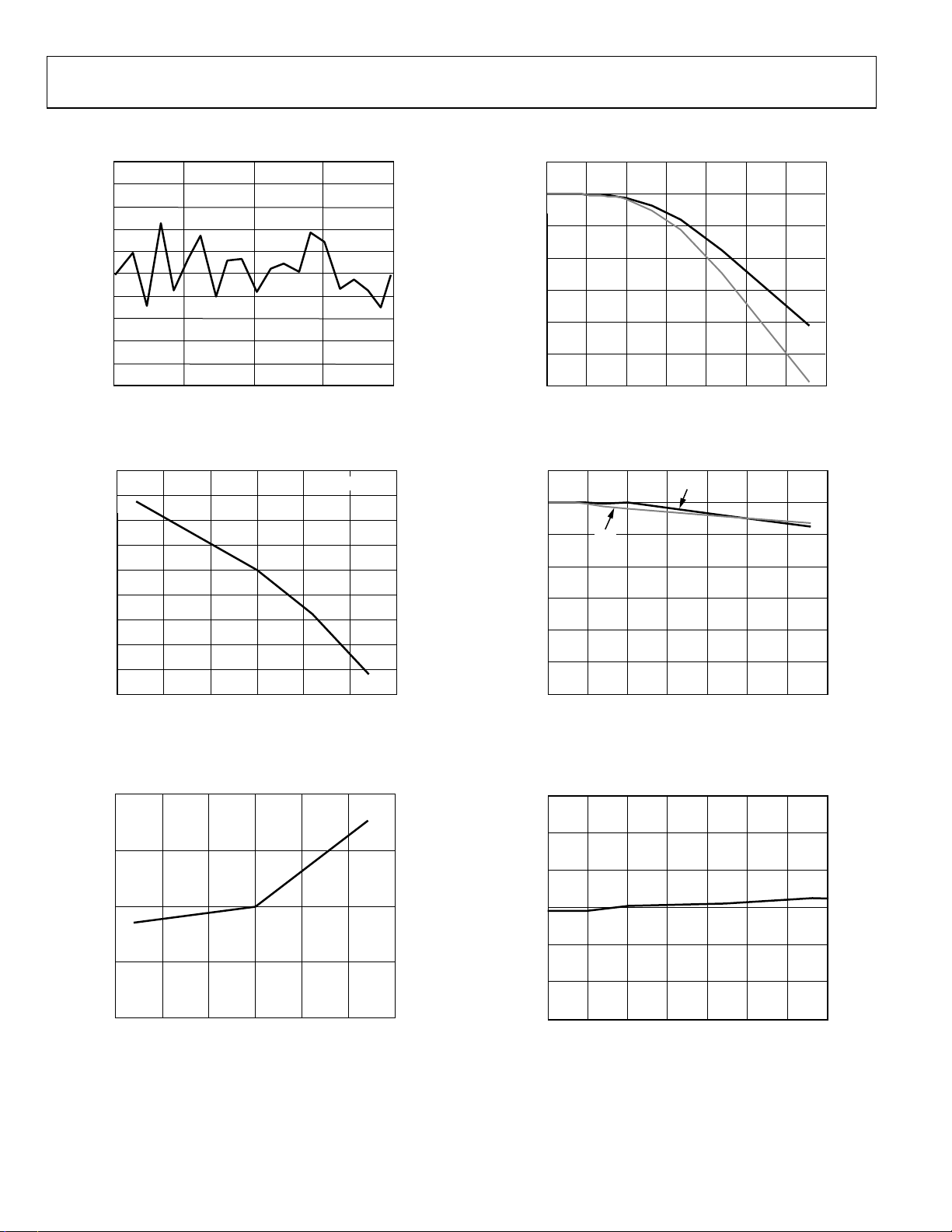
TYPICAL PERFORMANCE CHARACTERISTICS
0.05
0.04
0.03
0.02
0.01
0
0.01
0.02
0.03
0.04
0.05
–2 –1 0 1 2
CAPACITANCE (pF)
INL (% of FSR)
07450-106
Figure 6. Capacitance Input Integral Nonlinearity,
V
DD
= 3.3 V, See Figure 34
–0.25
–0.20
–0.15
–0.10
–0.05
0.00
0.05
0.10
0.15
0.20
50 25 0 25 50 75 100
TEMPERATURE (° C)
GAIN ERROR (%FS R)
07450-107
TC ≈ 28ppm/°C
Figure 7. Capacitance Input Gain Drift vs. Temperature,
V
DD
= 3.3 V, Range = ±2 pF
–0.4
–0.2
0
0.2
0.4
–50 –25 0 25 50 75 100
TEMPERATURE (°C)
OFFSET CAPACITANCE (fF )
07450-108
Figure 8. Capacitance Input Offset Drift vs. Temperature,
V
DD
= 3.3 V, CIN and EXC Pins Open Circuit
–12
–10
–8
–6
–4
–2
0
2
0 50 100 150 200 250 300 350
CAP LOAD TO GND (pF)
GAIN ERROR (%F SR)
3pF
9pF
07450-109
Figure 9. Capacitance Input Error vs. Capacitance Between CIN and GND;
Single-Ended Mode, CIN(+) to EXC = 3 pF and 9 pF, V
DD
= 3.3 V
–12
–10
–8
–6
–4
–2
0
2
0 50 100 150 200 250 300 350
CAP LOAD TO G ND (pF)
GAIN ERROR (%FS R)
2pF
07450-110
8pF
Figure 10. Capacitance Input Error vs. Capacitance Between CIN and GND,
Differential Mode, CIN(+) to EXC = 2 pF and 8 pF,
CIN(−) to EXC = 0 pF and 6 pF, V
DD
= 3.3 V
–0.3
–0.2
–0.1
0
0.1
0.2
0.3
0 50 100 150 200 250 300 350
CAP LOAD TO GND (pF)
GAIN ERROR (%F SR)
07450-111
Figure 11. Capacitance Input Error vs. Capacitance Between EXC and GND,
Single-Ended Mode, CIN(+) to EXC = 9 pF, V
DD
= 3.3 V
Loading...