


Analog Devices AD7226TQ, AD7226TE, AD7226KR, AD7226KP, AD7226KN Datasheet
...
a |
LC2MOS |
|
Quad 8-Bit D/A Converter |
||
|
|
AD7226 |
|
FEATURES |
FUNCTIONAL BLOCK DIAGRAM |
|
Four 8-Bit DACs with Output Amplifiers |
|
|
Skinny 20-Pin DIP, SOIC and 20-Terminal |
|
|
Surface Mount Packages |
|
|
Microprocessor Compatible |
|
|
TTL/CMOS Compatible |
|
|
No User Trims |
|
|
Extended Temperature Range Operation |
|
|
Single Supply Operation Possible |
|
|
APPLICATIONS |
|
|
Process Control |
|
|
Automatic Test Equipment |
|
|
Automatic Calibration of Large System Parameters, |
|
|
e.g., Gain/Offset |
|
GENERAL DESCRIPTION
The AD7226 contains four 8-bit voltage-output digital-to- analog converters, with output buffer amplifiers and interface logic on a single monolithic chip. No external trims are required to achieve full specified performance for the part.
Separate on-chip latches are provided for each of the four D/A converters. Data is transferred into one of these data latches through a common 8-bit TTL/CMOS (5 V) compatible input port. Control inputs A0 and A1 determine which DAC is loaded when WR goes low. The control logic is speed-compatible with most 8-bit microprocessors.
Each D/A converter includes an output buffer amplifier capable of driving up to 5 mA of output current. The amplifiers’ offsets are laser-trimmed during manufacture, thereby eliminating any requirement for offset nulling.
Specified performance is guaranteed for input reference voltages from +2 V to +12.5 V with dual supplies. The part is also specified for single supply operation at a reference of +10 V.
The AD7226 is fabricated in an all ion-implanted high speed Linear Compatible CMOS (LC2MOS) process which has been specifically developed to allow high speed digital logic circuits and precision analog circuits to be integrated on the same chip.
REV. A
Information furnished by Analog Devices is believed to be accurate and reliable. However, no responsibility is assumed by Analog Devices for its use, nor for any infringements of patents or other rights of third parties which may result from its use. No license is granted by implication or otherwise under any patent or patent rights of Analog Devices.
PRODUCT HIGHLIGHTS
1. DAC-to-DAC Matching
Since all four DACs are fabricated on the same chip at the same time, precise matching and tracking between the DACs is inherent.
2. Single Supply Operation
The voltage mode configuration of the DACs allows the AD7226 to be operated from a single power supply rail.
3. Microprocessor Compatibility
The AD7226 has a common 8-bit data bus with individual DAC latches, providing a versatile control architecture for simple interface to microprocessors. All latch enable signals are level triggered.
4. Small Size
Combining four DACs and four op amps plus interface logic into a 20-pin DIP or SOIC or a 20-terminal surface mount package allows a dramatic reduction in board space requirements and offers increased reliability in systems using multiple converters. Its pinout is aimed at optimizing board layout with all the analog inputs and outputs at one end of the package and all the digital inputs at the other.
One Technology Way, P.O. Box 9106, Norwood, MA 02062-9106, U.S.A. Tel: 617/329-4700 Fax: 617/326-8703
AD7226–SPECIFICATIONS
DUAL SUPPLY |
(VDD = 11.4 V to 16.5 V, VSS = –5 V 6 10%; AGND = DGND = O V; VREF = +2 V to (VDD – 4 V)1 unless otherwise noted. |
|||
All specifications TMIN to TMAX unless otherwise noted.) |
|
|||
Parameter |
|
K, B, T Versions2 |
Units |
Conditions/Comments |
|
|
|
|
|
STATIC PERFORMANCE |
|
|
|
|
Resolution |
|
8 |
Bits |
|
Total Unadjusted Error |
±2 |
LSB max |
VDD = +15 V ± 5%, VREF = +10 V |
|
Relative Accuracy |
|
±1 |
LSB max |
|
Differential Nonlinearity |
±1 |
LSB max |
Guaranteed Monotonic |
|
Full Scale Error |
|
±1 1/2 |
LSB max |
|
Full Scale Temperature Coefficient |
±20 |
ppm/°C typ |
VDD = 14 V to 16.5 V, VREF = +10 V |
|
Zero Code Error |
|
±30 |
mV max |
|
Zero Code Error Temperature Coefficient |
±50 |
μV/°C typ |
|
|
|
|
|
|
|
REFERENCE INPUT |
|
|
|
|
Voltage Range |
|
2 to (VDD – 4) |
V min to V max |
|
Input Resistance |
|
2 |
kΩ min |
|
Input Capacitance3 |
|
65 |
pF min |
Occurs when each DAC is loaded with all 0s. |
|
|
300 |
pF max |
Occurs when each DAC is loaded with all 1s. |
|
|
|
|
|
DIGITAL INPUTS |
|
|
|
|
Input High Voltage, VINH |
2.4 |
V min |
|
|
Input Low Voltage, VINL |
0.8 |
V max |
|
|
Input Leakage Current |
±1 |
μA max |
VIN = 0 V or VDD |
|
Input Capacitance |
|
8 |
pF max |
|
Input Coding |
|
Binary |
|
|
|
|
|
|
|
DYNAMIC PERFORMANCE |
|
V/μs min |
|
|
Voltage Output Slew Rate4 |
2.5 |
|
||
Voltage Output Settling Time4 |
|
μs max |
VREF = +10 V; Settling Time to ±1/2 LSB |
|
Positive Full Scale Change |
5 |
|||
Negative Full Scale Change |
7 |
μs max |
VREF = +10 V; Settling Time to ±1/2 LSB |
|
Digital Crosstalk |
|
50 |
nV secs typ |
|
Minimum Load Resistance |
2 |
kΩ min |
VOUT = +10 V |
|
|
|
|
|
|
POWER SUPPLIES |
|
|
|
|
VDD Range |
|
11.4/16.5 |
V min/V max |
For Specified Performance |
IDD |
|
13 |
mA max |
Outputs Unloaded; VIN = VINL or VINH |
ISS |
|
11 |
mA max |
Outputs Unloaded; VIN = VINL or VINH |
SWITCHING CHARACTERISTICS4, 5 |
|
|
|
|
Address to Write Setup Time, tAS |
|
|
|
|
@ 25°C |
|
0 |
ns min |
|
TMIN to TMAX |
|
0 |
ns min |
|
Address to Write Hold Time, tAH |
|
|
|
|
@ 25°C |
|
10 |
ns min |
|
TMIN to TMAX |
|
10 |
ns min |
|
Data Valid to Write Setup Time, tDS |
|
|
|
|
@ 25°C |
|
90 |
ns min |
|
TMIN to TMAX |
|
100 |
ns min |
|
Data Valid to Write Hold Time, tDH |
|
|
|
|
@ 25°C |
|
10 |
ns min |
|
TMIN to TMAX |
|
10 |
ns min |
|
Write Pulse Width, tWR |
|
|
|
|
@ 25°C |
|
150 |
ns min |
|
TMIN to TMAX |
|
200 |
ns min |
|
NOTES
1Maximum possible reference voltage.
2Temperature ranges are as follows: K Version: –40°C to +85°C
B Version: –40°C to +85°C T Version: –55°C to +125°C
3Guanteed by design. Not production tested. 4Sample Tested at 25°C to ensure compliance.
5Switching Characteristics apply for single and dual supply operation.
Specifications subject to change without notice.
–2– |
REV. A |

AD7226
(VDD = +15 V 6 5%; VSS = AGND = DGND = O V; VREF = +10 V1 unless otherwise noted. |
|||
SINGLE SUPPLY All specifications TMIN to TMAX unless otherwise noted.) |
|
||
Parameter |
K, B, T Versions2 |
Units |
Conditions/Comments |
|
|
|
|
STATIC PERFORMANCE |
|
|
|
Resolution |
8 |
Bits |
|
Total Unadjusted Error |
±2 |
LSB max |
|
Differential Nonlinearity |
± 1 |
LSB max |
Guaranteed Monotonic |
|
|
|
|
REFERENCE INPUT |
|
kΩ min |
|
Input Resistance |
2 |
|
|
Input Capacitance3 |
65 |
pF min |
Occurs when each DAC is loaded with all 0s. |
|
300 |
pF max |
Occurs when each DAC is loaded with all 1s. |
|
|
|
|
DIGITAL INPUTS |
|
|
|
Input High Voltage, VINH |
2.4 |
V min |
|
Input Low Voltage, VINL |
0.8 |
V max |
|
Input Leakage Current |
± 1 |
μA max |
VIN = 0 V or VDD |
Input Capacitance |
8 |
pF max |
|
Input Coding |
Binary |
|
|
|
|
|
|
DYNAMIC PERFORMANCE |
|
V/μs min |
|
Voltage Output Slew Rate4 |
2 |
|
|
Voltage Output Settling Time4 |
|
μs max |
Settling Time to ±1/2 LSB |
Positive Full Scale Change |
5 |
||
Negative Full Scale Change |
20 |
μs max |
Settling Time to ±1/2 LSB |
Digital Crosstalk |
50 |
nV secs typ |
|
Minimum Load Resistance |
2 |
kΩ min |
VOUT = +10 V |
|
|
|
|
POWER SUPPLIES |
|
|
|
VDD Range |
14.25/15.75 |
V min/V max |
For Specified Performance |
IDD |
13 |
mA max |
Outputs Unloaded; VIN = VINL or VINH |
NOTES
1Maximum possible reference voltage.
2Temperature ranges are as follows: K Version: –40°C to +85°C
B Version: –40°C to +85°C T Version: –55°C to +125°C
3Guanteed by design. Not production tested. 4Sample Tested at 25°C to ensure compliance.
5Switching Characteristics apply for single and dual supply operation.
Specifications subject to change without notice.
ORDERING GUIDE
|
|
Total |
|
|
Temperature |
Unadjusted |
Package |
Model1 |
Range |
Error |
Option2 |
|
|
|
|
AD7226KN |
–40°C to +85°C |
±2 LSB |
N-20 |
AD7226KP |
–40°C to +85°C |
±2 LSB |
P-20A |
AD7226KR |
–40°C to +85°C |
±2 LSB |
R-20 |
AD7226BQ |
–40°C to +85°C |
±2 LSB |
Q-20 |
AD7226TQ |
–55°C to +125°C |
±2 LSB |
Q-20 |
AD7226TE |
–55°C to +125°C |
±2 LSB |
E-20A |
NOTES
1To order MIL-STD-883, Class B processed parts, add /883B to part number. Contact your local sales office for Military data sheet, for U.S. Standard Military Drawing (SMD), see DESC drawing #5962–87802.
2E = Leadless Ceramic Chip Carrier; N = Plastic DIP;
P = Plastic Leaded Chip Carrier; Q = Cerdip; R = SOIC.
REV. A |
–3– |
AD7226
ABSOLUTE MAXIMUM RATINGS* |
|
|
|
||
VDD to AGND . . . . . . . . . . . . . . . . . . . . . |
. . . . . |
–0.3 V, +17 V |
|||
VDD to DGND . . . . . . . . . . . . . . . . . . . . . . |
. . . . |
–0.3 V, +17 V |
|||
VSS to AGND . . . . . . . . . . . . . . . . . . . . . . |
. . . . |
. . . –7 V, VDD |
|||
VSS to DGND . . . . . . . . . . . . . . . . . . . . . . |
. . . . |
. . . –7 V, VDD |
|||
VDD to VSS . . . . . . . . . . . . . . . . . . . . . . . . . |
. . . . |
–0.3 V, +24 V |
|||
AGND to DGND . . . . . . . . . . . . . . . . . . . |
. . . . |
. –0.3 V, VDD |
|||
Digital Input Voltage to DGND . . . . . . . |
–0.3 V, VDD + 0.3 V |
||||
VREF to AGND . . . . . . . . . . . . . . . . . . . . . |
. . . . |
. –0.3 V, VDD |
|||
V |
OUT |
to AGND1 . . . . . . . . . . . . . . . . . . . . |
. . . . |
. . . . V |
, V |
|
|
|
SS |
DD |
|
Power Dissipation (Any Package) to +75°C . . . . |
. . . . 500 mW |
||||
Derates above 75°C by . . . . . . . . . . . . . . . |
. . . . |
. . 2.0 mW/°C |
|||
Operating Temperature |
–40°C to +85°C |
Commercial (K Version) . . . . . . . . . . . . . |
|
Industrial (B Version) . . . . . . . . . . . . . . . . |
–40°C to +85°C |
Extended (T Version) . . . . . . . . . . . . . . . |
–55°C to +125°C |
Storage Temperature . . . . . . . . . . . . . . . . . . |
–65°C to +150°C |
Lead Temperature (Soldering, 10 secs) . . . . . |
. . . . . . +300°C |
NOTES
*Stresses above those listed under “Absolute Maximum Ratings” may cause permanent damage to the device. This is a stress rating only and functional operation of the device at these or any other conditions above those indicated in the operational sections of this specification is not implied. Exposure to absolute maximum rating conditions for extended periods may affect device reliability.
1Outputs may be shorted to AGND provided that the power dissipation of the package is not exceeded. Typically short circuit current to AGND is 60 mA.
CAUTION
ESD (electrostatic discharge) sensitive device. Electrostatic charges as high as 4000 V readily accumulate on the human body and test equipment and can discharge without detection. Although the AD7226 features proprietary ESD protection circuitry, permanent damage may occur on devices subjected to high energy electrostatic discharges. Therefore, proper ESD precautions are recommended to avoid performance degradation or loss of functionality.
|
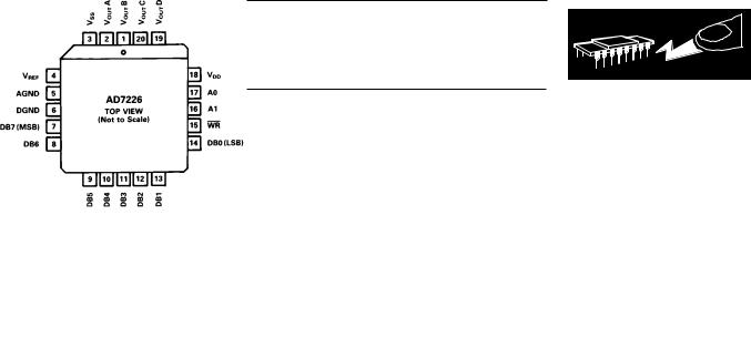
PIN CONFIGURATIONS |
DIP and SOIC |
LCCC |
WARNING!
ESD SENSITIVE DEVICE
PLCC
TERMINOLOGY
TOTAL UNADJUSTED ERROR
This is a comprehensive specification which includes full-scale error, relative accuracy and zero code error. Maximum output
voltage is VREF – 1 LSB (ideal), where 1 LSB (ideal) is VREF/ 256. The LSB size will vary over the VREF range. Hence the zero
code error will, relative to the LSB size, increase as VREF decreases. Accordingly, the total unadjusted error, which includes the zero code error, will also vary in terms of LSB’s over the VREF range. As a result, total unadjusted error is specified for a fixed reference voltage of +10 V.
RELATIVE ACCURACY
Relative Accuracy or endpoint nonlinearity, is a measure of the maximum deviation from a straight line passing through the endpoints of the DAC transfer function. It is measured after allowing for zero and full-scale error and is normally expressed in LSB’s or as a percentage of full-scale reading.
DIFFERENTIAL NONLINEARITY
Differential Nonlinearity is the difference between the measured change and the ideal 1 LSB change between any two adjacent codes. A specified differential nonlinearity of ±1 LSB max over the operating temperature range ensures monotonicity.
DIGITAL CROSSTALK
The glitch impulse transferred to the output of one converter due to a change in the digital input code to another of the converters. It is specified in nV secs and is measured at VREF = 0 V.
FULL SCALE ERROR
Full-Scale Error is defined as:
Measured Value – Zero Code Error – Ideal Value
–4– |
REV. A |
 Loading...