


Analog Devices AD7228ATQ, AD7228ACR, AD7228ACQ, AD7228ACP, AD7228ACN Datasheet
...
a |
LC2MOS |
|
Octal 8-Bit DAC |
||
|
|
AD7228A |
FEATURES
Eight 8-Bit DACs with Output Amplifiers Operates with Single +5 V, +12 V or +15 V
or Dual Supplies
mP Compatible (95 ns WR Pulse)
No User Trims Required
Skinny 24-Pin DlPs, SOIC, and 28-Terminal Surface Mount Packages
GENERAL DESCRIPTION
The AD7228A contains eight 8-bit voltage-mode digital-to- analog converters, with output buffer amplifiers and interface logic on a single monolithic chip. No external trims are required to achieve full specified performance for the part.
Separate on-chip latches are provided for each of the eight D/A converters. Data is transferred into the data latches through a common 8-bit TTL/CMOS (5 V) compatible input port. Address inputs A0, A1 and A2 determine which latch is loaded when WR goes low. The control logic is speed compatible with most 8-bit microprocessors.
Specified performance is guaranteed for input reference voltages from +2 to +10 V when using dual supplies. The part is also specified for single supply +15 V operation using a reference of +10 V and single supply +5 V operation using a reference of +1.23 V. Each output buffer amplifier is capable of developing +10 V across a 2 kΩ load.
The AD7228A is fabricated on an all ion-implanted, highspeed, Linear Compatible CMOS (LC2MOS) process which has been specifically developed to integrate high-speed digital logic circuits and precision analog circuits on the same chip.
REV. A
Information furnished by Analog Devices is believed to be accurate and reliable. However, no responsibility is assumed by Analog Devices for its use, nor for any infringements of patents or other rights of third parties which may result from its use. No license is granted by implication or otherwise under any patent or patent rights of Analog Devices.
FUNCTIONAL BLOCK DIAGRAM
PRODUCT HIGHLIGHTS
1. Eight DACs and Amplifiers in Small Package
The single-chip design of eight 8-bit DACs and amplifiers allows a dramatic reduction in board space requirements and offers increased reliability in systems using multiple converters. Its pinout is aimed at optimizing board layout with all analog inputs and outputs at one side of the package and all digital inputs at the other.
2. Single or Dual Supply Operation
The voltage-mode configuration of the DACs allows single supply operation of the AD7228A. The part can also be operated with dual supplies giving enhanced performance for some parameters.
3. Microprocessor Compatibility
The AD7228A has a common 8-bit data bus with individual DAC latches, providing a versatile control architecture for simple interface to microprocessors. All latch enable signals are level triggered and speed compatible with most high performance 8-bit microprocessors.
One Technology Way, P.O. Box 9106, Norwood, MA 02062-9106, U.S.A. Tel: 617/329-4700 Fax: 617/326-8703
AD7228A–SPECIFICATIONS
(VDD = 10.8 V to 16.5 V; VSS = –5 V 6 10%; GND = 0 V; VREF = +2 V to +10 V1; RL = 2 kΩ, CL = 100 pF unless otherwise |
|||||||||
DUAL SUPPLY noted.) |
All specifications TMIN to TMAX unless otherwise noted. |
|
|
|
|||||
|
|
B |
C |
T |
U |
|
|
|
|
Parameter |
|
Version2 |
Version |
Version |
Version |
Units |
Conditions/Comments |
||
STATIC PERFORMANCE |
|
|
|
|
|
|
|
|
|
Resolution |
|
8 |
8 |
8 |
8 |
Bits |
|
|
|
Total Unadjusted Error3 |
|
± 2 |
± 1 |
± 2 |
± 1 |
LSB max |
VDD = +15 V ± 10%, VREF = +10 V |
||
Relative Accuracy |
|
± 1 |
± 1/2 |
± 1 |
± 1/2 |
LSB max |
|
|
|
Differential Nonlinearity |
|
± 1 |
± 1 |
± 1 |
± 1 |
LSB max |
Guaranteed Monotonic |
||
Full-Scale Error4 |
|
± 1 |
± 1/2 |
± 1 |
± 1/2 |
LSB max |
Typical tempco is 5 ppm/°C with VREF = +10 V |
||
Zero Code Error |
|
|
|
|
|
|
|
|
|
@ 25°C |
|
± 25 |
± 15 |
± 25 |
± 15 |
mV max |
Typical tempco is 30 μV/°C |
||
TMIN to TMAX |
|
± 30 |
± 20 |
± 30 |
± 20 |
mV max |
|
|
|
Minimum Load Resistance |
|
2 |
2 |
2 |
2 |
kΩ min |
VOUT = +10 V |
||
REFERENCE INPUT |
|
|
|
|
|
|
|
|
|
Voltage Range1 |
|
2 to 10 |
2 to 10 |
2 to 10 |
2 to 10 |
V min/V max |
|
|
|
Input Resistance |
|
2 |
2 |
2 |
2 |
kΩ min |
|
|
|
Input Capacitance5 |
|
500 |
500 |
500 |
500 |
pF max |
Occurs when each DAC is loaded with all 1s. |
||
AC Feedthrough |
|
–70 |
–70 |
–70 |
–7 0 |
dB typ |
VREF = 8 V p-p Sine Wave @ 10 kHz |
||
DIGITAL INPUTS |
|
|
|
|
|
|
|
|
|
Input High Voltage, VINH |
|
2.4 |
2.4 |
2.4 |
2.4 |
V min |
|
|
|
Input Low Voltage, VINL |
|
0.8 |
0.8 |
0.8 |
0.8 |
V max |
|
|
|
Input Leakage Current |
|
± 1 |
± 1 |
± 1 |
± 1 |
μA max |
VIN = 0 V or VDD |
||
Input Capacitance5 |
|
8 |
8 |
8 |
8 |
pF max |
|
|
|
Input Coding |
|
Binary |
Binary |
Binary |
Binary |
|
|
|
|
|
|
|
|
|
|
|
|
|
|
DYNAMIC PERFORMANCE5 |
|
|
|
|
|
V/μs min |
|
|
|
Voltage Output Slew Rate |
|
2 |
2 |
2 |
2 |
|
|
|
|
Voltage Output Settling Time |
|
|
|
|
|
μs max |
VREF = +10 V; Settling Time to ± 1/2 LSB |
||
Positive Full-Scale Change |
|
5 |
5 |
5 |
5 |
||||
Negative Full-Scale Change |
|
5 |
5 |
5 |
5 |
μs max |
VREF = +10 V; Settling Time to ± 1/2 LSB |
||
Digital Feedthrough |
|
50 |
50 |
50 |
50 |
nV secs typ |
Code transition all 0s to all 1s. VREF = 0 V; |
WR |
= VDD |
Digital Crosstalk6 |
|
50 |
50 |
50 |
50 |
nV secs typ |
Code transition all 0s to all 1s. VREF = +10 V; WR = 0 V |
||
POWER SUPPLIES |
|
|
|
|
|
|
|
|
|
VDD Range |
|
10.8/16.5 |
10.8/16.5 |
10.8/16.5 |
10.8/16.5 |
V min/V max |
For Specified Performance |
||
VSS Range |
|
–4.5/–5.5 |
–4.5/–5.5 |
–4.5/–5.5 |
–4.5/–5.5 |
V min/V max |
For Specified Performance |
||
IDD |
|
|
|
|
|
|
Outputs Unloaded; VIN = VINL or VINH |
||
@ 25°C |
|
16 |
16 |
16 |
16 |
mA max |
|
|
|
TMIN to TMAX |
|
20 |
20 |
22 |
22 |
mA max |
|
|
|
ISS |
|
|
|
|
|
|
Outputs Unloaded; VIN = VINL or VINH |
||
@ 25°C |
|
14 |
14 |
14 |
14 |
mA max |
|
|
|
TMIN to TMAX |
|
18 |
18 |
20 |
20 |
mA max |
|
|
|
(VDD = +15 V 6 10%, VSS; = GND = 0 V; VREF = +10 V, RL = 2 kΩ, CL = 100 pF unless otherwise noted.) |
|||||||||
SINGLE SUPPLY AII specifications TMIN to TMAX unless otherwise noted. |
|
|
|
||||||
STATIC PERFORMANCE |
|
|
|
|
|
|
|
|
|
Resolution |
|
8 |
8 |
8 |
8 |
Bits |
|
|
|
Total Unadjusted Error3 |
|
± 2 |
± 1 |
± 2 |
± 1 |
LSB max |
|
|
|
Differential Nonlinearity |
|
± 1 |
± 1 |
± 1 |
± 1 |
LSB max |
Guaranteed Monotonic |
||
Minimum Load Resistance |
|
2 |
2 |
2 |
2 |
kΩ min |
VOUT = +10 V |
||
REFERENCE INPUT |
|
|
|
|
|
kΩ min |
|
|
|
Input Resistance |
|
2 |
2 |
2 |
2 |
|
|
|
|
Input Capacitance5 |
|
500 |
500 |
500 |
500 |
pF max |
Occurs when each DAC is loaded with all 1s. |
||
DIGITAL INPUTS |
|
As per Dual Supply Specifications |
|
|
|
|
|||
|
|
|
|
|
|
|
|
|
|
DYNAMIC PERFORMANCE5 |
|
|
|
|
|
V/μs min |
|
|
|
Voltage Output Slew Rate |
|
2 |
2 |
2 |
2 |
|
|
|
|
Voltage Output Settling Time |
|
|
|
|
|
μs max |
Settling Time to ±1/2 LSB |
||
Positive Full-Scale Change |
|
5 |
5 |
5 |
5 |
||||
Negative Full-Scale Change |
|
7 |
7 |
7 |
7 |
μs max |
Settling Time to ±1/2 LSB |
||
Digital Feedthrough |
|
50 |
50 |
50 |
50 |
nV secs typ |
Code transition all 0s to all 1s. VREF = 0 V; |
WR |
= VDD |
Digital Crosstalk6 |
|
50 |
50 |
50 |
50 |
nV secs typ |
Code transition all 0s to all 1s. VREF = +10 V, WR = 0 V |
||
POWER SUPPLIES |
|
|
|
|
|
|
|
|
|
VDD Range |
|
13.5/16.5 |
13.5/16.5 |
13.5/16.5 |
13.5/16.5 |
V min/V max |
For Specified Performance |
||
IDD |
|
|
|
|
|
|
Outputs Unloaded; VIN = VINL or VINH |
||
@ 25°C |
|
16 |
16 |
16 |
16 |
mA max |
|
|
|
TMIN to TMAX |
|
20 |
20 |
22 |
22 |
mA max |
|
|
|
NOTES
1VOUT must be less than VDD by 3.5 V to ensure correct operation. 2Temperature ranges are as follows:
B, C Versions; –40°C to +85°C T, U Versions; –55°C to +125°C
3Total Unadjusted Error includes zero code error, relative accuracy and full-scale error. 4Calculated after zero code error has been adjusted out.
5Sample tested at 25°C to ensure compliance.
6The glitch impulse transferred to the output of one converter (not addressed) due to a change in the digital input code to another addressed converter.
Specifications subject to change without notice.
–2– |
REV. A |
|
|
|
|
|
|
|
|
|
|
|
|
|
|
|
|
|
AD7228A |
|
|
|
|
|
|
(VDD = +5 V 6 5%, VSS; = 0 to –5 V 6 10%, GND = 0 V, VREF = +1.25 V, RL = 2 kV, CL = 100 pF |
|||||||||||||
+5 V SUPPLY OPERATION unless otherwise noted.) AII specifications TMIN to TMAX unless otherwise noted. |
||||||||||||||||||
|
|
|
|
B |
|
C |
|
T |
U |
|
|
|
|
|
|
|||
Parameter |
|
|
Version |
|
Version |
Version |
Version |
Units |
|
Conditions/Comments |
||||||||
|
|
|
|
|
|
|
|
|
|
|
|
|
|
|
|
|
|
|
STATIC PERFORMANCE |
|
|
|
|
|
|
|
|
|
|
|
|
|
|
|
|
|
|
Resolution |
|
|
8 |
|
|
8 |
|
8 |
8 |
|
Bits |
|
|
|
|
|||
Relative Accuracy |
|
|
± 2 |
|
|
± 2 |
|
± 2 |
± 2 |
|
LSB max |
|
|
|
|
|||
Differential Nonlinearity |
|
|
± 1 |
|
|
± 1 |
|
± 1 |
± 1 |
|
LSB max |
|
Guaranteed Monotonic |
|||||
Full-Scale Error |
|
|
± 4 |
|
|
± 2 |
|
± 4 |
± 2 |
|
LSB max |
|
|
|
|
|||
Zero Code Error |
|
|
± 30 |
|
|
± 20 |
|
± 30 |
± 20 |
|
|
|
|
|
|
|
||
@ 25°C |
|
|
|
|
|
|
mV max |
|
|
|
|
|||||||
TMIN to TMAX |
|
|
± 40 |
|
|
± 30 |
|
± 40 |
± 30 |
|
mV max |
|
|
|
|
|||
REFERENCE INPUT |
|
|
|
|
|
|
|
|
|
|
|
|
|
|
|
|
|
|
Reference Input Range |
|
|
1.2 |
|
|
1.2 |
|
1.2 |
1.2 |
|
V min |
|
|
|
|
|||
|
|
|
|
1.3 |
|
|
1.3 |
|
1.3 |
1.3 |
|
V max |
|
|
|
|
||
Reference Input Resistance |
|
2 |
|
|
2 |
|
2 |
2 |
|
kΩ min |
|
|
|
|
||||
Reference Input Capacitance |
|
500 |
|
|
500 |
|
500 |
500 |
|
pF max |
|
|
|
|
||||
|
|
|
|
|
|
|
|
|
|
|
|
|
|
|
|
|
|
|
POWER REQUIREMENTS |
|
|
|
|
|
|
|
|
|
|
|
|
|
|
|
|
||
Positive Supply Range |
|
|
4.75/5.25 |
|
4.75/5.25 |
4.75/5.25 |
4.75/5.25 |
|
V min/V max |
|
For Specified Performance |
|||||||
Positive Supply Current |
|
|
|
|
|
|
|
|
|
|
|
μA max |
|
|
|
|
||
@ 25°C |
|
|
16 |
|
|
16 |
|
16 |
16 |
|
|
|
|
|
||||
TMIN to TMAX |
|
|
20 |
|
|
20 |
|
22 |
22 |
|
μA max |
|
|
|
|
|||
Negative Supply Current |
|
|
|
|
|
|
|
|
|
|
|
μA max |
|
|
|
|
||
@ 25°C |
|
|
14 |
|
|
14 |
|
14 |
14 |
|
|
|
|
|
||||
TMIN to TMAX |
|
|
18 |
|
|
18 |
|
20 |
20 |
|
μA max |
|
|
|
|
|||
NOTES |
|
|
|
|
|
|
|
|
|
|
|
|
|
|
|
|
|
|
All of the specifications as per Dual Supply Specifications except for negative full-scale settling-time when VSS = 0 V. |
|
|
|
|
|
|
||||||||||||
Specifications subject to change without notice. |
|
|
|
|
|
|
|
|
|
|
|
|
|
|||||
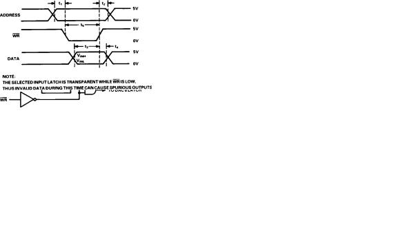
SWITCHING CHARACTERISTICS1, 2 |
(See Figures 1, 2; VDD = +5 V 6 5% or +10.8 V to +16.5 V; VSS = 0 V or –5 V 6 10%) |
|||||||||||||||||
|
Limit at 25°C |
|
Limit at TMIN, TMAX |
|
Limit at TMIN, TMAX |
|
|
|
|
|
|
|
||||||
Parameters |
|
All Grades |
|
(B, C Versions) |
|
(T, U Versions) |
|
Units |
|
Conditions/Comments |
||||||||
|
|
|
|
|
|
|
|
|
|
|
|
|
|
|
|
|
|
|
t1 |
|
|
0 |
|
|
0 |
|
|
|
0 |
|
ns min |
|
Address to |
|
Setup Time |
||
|
|
|
|
WR |
||||||||||||||
t2 |
|
|
0 |
|
|
0 |
|
|
|
0 |
|
ns min |
|
Address to WR Hold Time |
||||
t3 |
|
|
70 |
|
|
90 |
|
|
|
100 |
|
ns min |
|
Data Valid to WR Setup Time |
||||
t4 |
|
|
10 |
|
|
10 |
|
|
|
10 |
|
ns min |
|
Data Valid to WR Hold Time |
||||
t5 |
|
|
95 |
|
|
120 |
|
|
150 |
|
ns min |
|
Write Pulse Width |
|||||
NOTES
1Sample tested at 25°C to ensure compliance. All input rise and fall times measured from 10% to 90% of +5 V, tR = tF = 5 ns.
2Timing measurement reference level is |
V INH +V INL |
|
2 |
||
|
INTERFACE LOGIC INFORMATION
Address lines A0, A1 and A2 select which DAC accepts data from the input port. Table I shows the selection table for the eight DACs with Figure 1 showing the input control logic.
When the WR signal is low, the input latch of the selected DAC is transparent, and its output responds to activity on the data bus. The data is latched into the addressed DAC latch on the rising edge of WR. While WR is high, the analog outputs remain at the value corresponding to the data held in their respective latches.
Table I. AD7228A Truth Table
|
AD7228A Control Inputs |
|
|
AD7228A |
Figure 1. Input Control Logic |
||
|
WR |
A2 |
A1 |
A0 |
|
Operation |
|
|
|
|
|||||
|
|
|
|
|
|
|
|
|
H |
X |
X |
X |
|
No Operation |
|
|
|
|
|
|
|
Device Not Selected |
|
|
L |
L |
L |
L |
|
DAC 1 Transparent |
|
|
g |
L |
L |
L |
|
DAC 1 Latched |
|
|
L |
L |
L |
H |
|
DAC 2 Transparent |
|
|
L |
L |
H |
L |
|
DAC 3 Transparent |
|
|
L |
L |
H |
H |
|
DAC 4 Transparent |
|
|
L |
H |
L |
L |
|
DAC 5 Transparent |
|
|
L |
H |
L |
H |
|
DAC 6 Transparent |
|
|
L |
H |
H |
L |
|
DAC 7 Transparent |
|
|
L |
H |
H |
H |
|
DAC 8 Transparent |
|
|
|
|
|
|
|
|
|
|
H = High State |
L = Low State |
X = Don’t Care |
|
Figure 2. Write Cycle Timing Diagram |
||
|
|
|
|
|
|
|
|
REV. A |
|
|
|
|
|
–3– |
|
 Loading...