


AD7142
Programmable Capacitance-to-Digital
Converter with Environmental Compensation
Preliminary Technical Data |
AD7142/AD7142-1 |
|
|
FEATURES
Programmable capacitance-to-digital converter 30 Hz update rate (@ maximum sequence length) Better than one femto Farad resolution
14 capacitance sensor input channels
No external RC tuning components required Automatic conversion sequencer
On-chip automatic calibration logic
Automatic compensation for environmental changes Automatic adaptive threshold and sensitivity levels
On-chip RAM to store calibration data
SPI®- or I2C®- (AD7142-1) compatible serial interface Separate VDRIVE level for serial interface
Interrupt output and GPIO 32-lead, 5 mm x 5 mm LFCSP 2.7 V to 3.3 V supply voltage Low operating current
Full power mode: less than1 mA Low power mode: 50 μA
APPLICATIONS
Personal music and multimedia players
Cell phones
Digital still cameras
Smart hand-held devices
Television, A/V and remote controls
Gaming consoles
FUNCTIONAL BLOCK DIAGRAM
|
|
|
VREF– VREF+ |
|
TEST |
|
|
||
|
|
|
29 |
28 |
|
27 |
|
|
|
CIN0 |
30 |
|
|
|
|
|
POWER-ON |
|
|
CIN1 |
31 |
|
|
|
|
|
RESET |
|
|
|
|
|
|
|
LOGIC |
|
|
||
CIN2 |
32 |
|
|
|
|
|
|
|
|
|
|
|
|
|
|
|
|
||
CIN3 |
1 |
|
|
|
|
|
|
13 |
AVCC |
CIN4 |
2 |
|
|
|
|
|
|
||
|
|
|
|
|
|
|
|
||
CIN5 |
3 |
SWITCH MATRIX |
|
|
|
|
|
14 |
AGND |
CIN6 |
4 |
16-BIT |
|
CALIBRATION |
|
|
|
||
CIN7 |
5 |
Σ- |
|
|
ENGINE |
|
|
|
|
CDC |
|
|
|
|
|
||||
CIN8 |
|
|
|
|
|
|
|||
6 |
|
|
|
|
|
|
|
||
|
|
|
|
|
|
|
|
||
CIN9 |
7 |
|
|
|
|
|
|
17 |
DVCC |
CIN10 |
8 |
|
AD7142 |
|
|
|
|
|
|
CIN11 |
9 |
|
|
CALIBRATION |
|
18 |
DGND1 |
||
CIN12 |
10 |
|
|
|
|
RAM |
|
|
|
|
|
|
|
|
|
19 |
DGND2 |
||
CIN13 |
11 |
|
CONTROL |
|
|
|
|||
|
|
|
AND |
|
|
|
|
|
|
|
|
|
DATA |
|
|
|
|
|
|
|
|
|
REGISTERS |
|
|
|
|
|
|
CSHIELD |
|
|
|
|
|
|
|
|
|
|
12 |
|
|
|
|
|
|
|
|
|
|
240kHz |
|
|
|
|
|
|
|
SRC |
15 |
EXCITATION |
|
|
|
|
|
|
|
|
|
SOURCE |
|
|
|
|
|
|
|
SRC |
16 |
|
|
|
|
|
|
|
|
VDRIVE |
|
SERIAL INTERFACE |
INTERRUPT |
|
|
||||
20 |
|
AND GPIO |
26 |
GPIO |
|||||
|
|
AND CONTROL LOGIC |
LOGIC |
|
|
||||
|
|
21 |
22 |
23 |
|
24 |
25 |
|
-001 |
|
|
|
|
05702 |
|||||
|
|
SDO/ |
SDI/ |
SCLK |
CS/ |
INT |
|
||
|
|
|
|
||||||
|
|
SDA |
ADD0 |
ADD1 |
|
|
|
||
Figure 1.
GENERAL DESCRIPTION
The AD7142 and AD7142-1 are integrated capacitance-to- digital converters (CDCs) with on-chip environmental calibration for use in systems requiring a novel user input method. The AD7142 and AD7142-1 can interface to external capacitance sensors implementing functions such as capacitive buttons, scroll bars, or joypads.
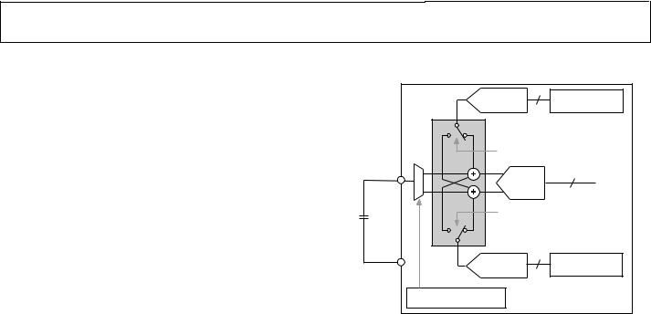
The CDC has 14 inputs, channeled through a switch matrix to a 16-bit, 240 kHz sigma-delta (∑-Δ) capacitance-to-digital converter. The CDC is capable of sensing changes in the capacitance of the external sensors and uses this information to register a sensor activation. The external sensors can be arranged as a series of buttons, as a scroll bar or wheel, or as a combination of sensor types. By programming the registers, the user has full control over the CDC setup. High resolution scroll bar sensors require software to run on the host processor.
Rev. PrD
Information furnished by Analog Devices is believed to be accurate and reliable. However, no responsibilityisassumedbyAnalogDevicesforitsuse,norforanyinfringementsofpatentsorother rightsofthirdpartiesthatmayresultfromitsuse.Specificationssubjecttochangewithoutnotice.No license is granted by implication or otherwise under any patent or patent rights of Analog Devices. Trademarksandregisteredtrademarksarethepropertyoftheirrespectiveowners.
The AD7142 and AD7142-1 have on-chip calibration logic to account for changes in the ambient environment. The calibration sequence is performed automatically and at continuous intervals, while the sensors are not touched. This ensures that there are no false or nonregistering touches on the external sensors due to a changing environment.
The AD7142 has an SPI-compatible serial interface, and the AD7142-1 has an I2C-compatible serial interface. Both versions of AD7142 have an interrupt output, as well as a general-purpose input output (GPIO).
The AD7142 and AD7142-1 are available in a 32-lead, 5 mm × 5 mm LFCSP package and operate from a 2.7 V to 3.3 V supply. The operating current consumption is less than 1 mA, falling to 50 μA in low power mode (conversion interval of 400 ms).
One Technology Way, P.O. Box 9106, Norwood, MA 02062-9106, U.S.A.
Tel: 781.329.4700 |
www.analog.com |
Fax: 781.461.3113 |
© 2005 Analog Devices, Inc. All rights reserved. |

AD7142/AD7142-1 |
Preliminary Technical Data |
TABLE OF CONTENTS |
|
Features .............................................................................................. |
1 |
Applications....................................................................................... |
1 |
Functional Block Diagram .............................................................. |
1 |
General Description......................................................................... |
1 |
Revision History ............................................................................... |
2 |
Specifications..................................................................................... |
3 |
SPI Timing Specifications AD7142............................................ |
4 |
I2C Timing Specifications AD7142-1 ........................................ |
5 |
Absolute Maximum Ratings............................................................ |
6 |
ESD Caution.................................................................................. |
6 |
Pin Configuration and Functional Descriptions......................... |
7 |
Typical Performance Characteristics ............................................. |
8 |
Theory of Operation ........................................................................ |
9 |
Capacitance Sensing Theory....................................................... |
9 |
Operating Modes........................................................................ |
10 |
Capacitance Sensor Input Configuration.................................... |
11 |
CIN Input Multiplexer Setup .................................................... |
11 |
Capacitiance-to-Digital Converter............................................... |
12 |
Oversampling the CDC Output ............................................... |
12 |
Capacitance Sensor Offset Control.......................................... |
12 |
Conversion Sequencer ............................................................... |
12 |
CDC Conversion Time.............................................................. |
13 |
CDC Conversion Results........................................................... |
14 |
Non-Contact Proximity Detection............................................... |
15 |
Environmental Calibration ........................................................... |
19 |
REVISION HISTORY
12/05—Preliminary Version D
7/05—Preliminary Version C
2/05—Preliminary Version B
Adaptive Threshold and Sensitivity ............................................. |
20 |
Interrupt Output............................................................................. |
21 |
CDC Conversion Complete Interrupt..................................... |
21 |
Sensor Threshold Interrupt ...................................................... |
21 |
GPIO INT Output Control ....................................................... |
22 |
Outputs ............................................................................................ |
24 |
Excitation Source........................................................................ |
24 |
CSHIELD Output ............................................................................. |
24 |
GPIO ............................................................................................ |
24 |
Serial Interface ................................................................................ |
25 |
SPI Interface ................................................................................ |
25 |
I2C Interface ................................................................................ |
27 |
VDRIVE Input ................................................................................. |
29 |
PCB Design Guidelines ................................................................. |
30 |
Capacitive Sensor Board Mechanical Specifications ............. |
30 |
Chip Scale Packages ................................................................... |
30 |
Power-Up Sequence ....................................................................... |
31 |
Typical Application Circuits ......................................................... |
32 |
Register Map ................................................................................... |
33 |
Detailed Register Descriptions ..................................................... |
34 |
Bank 1 Registers ......................................................................... |
34 |
Bank 2 Registers ......................................................................... |
44 |
Bank 3 Registers ......................................................................... |
47 |
Outline Dimensions ....................................................................... |
62 |
Ordering Guide .......................................................................... |
62 |
1/05—Preliminary Version A |
|
Rev. PrD | Page 2 of 64

Preliminary Technical Data |
AD7142/AD7142-1 |
|
|
SPECIFICATIONS
VCC = 2.7 V to 3.3 V, TA = −40oC to +85°C, unless otherwise noted.
Table 1.
Parameter |
Min |
Typ |
Max |
Unit |
Test Conditions/Comments |
||||
|
|
|
|
|
|
|
|
|
|
CAPACITANCE-TO-DIGITAL CONVERTER |
|
|
|
|
|
||||
Update Rate |
30 |
|
|
Hz |
Maximum programmed sequence length |
||||
Resolution |
|
16 |
|
Bit |
|
||||
Range |
|
±2 |
|
pF |
|
||||
No Missing Codes |
16 |
|
|
Bit |
Guaranteed by design, but not production |
||||
|
|
|
|
|
|
|
|
|
tested |
Total Unadjusted Error |
|
|
TBD |
fF |
|
||||
Power Supply Rejection |
|
500 |
|
aF/V |
|
||||
Output Noise (Peak-to-Peak) |
|
10 |
|
aF/√Hz |
|
||||
Parasitic Capacitance |
|
|
60 |
pF |
Parasitic capacitance to ground, guaranteed |
||||
|
|
|
|
|
|
|
|
|
by characterization |
|
|
|
|
|
|
|
|
|
|
EXCITATION SOURCE |
|
|
|
|
|
||||
Frequency |
TBD |
240 |
TBD |
kHz |
|
||||
Output Voltage |
|
|
AVCC |
V |
|
||||
Short-Circuit Current |
|
10 |
|
mA |
|
||||
Maximum Output Load |
|
500 |
|
pF |
Capacitance load on source to ground |
||||
CSHIELD Output Drive |
|
10 |
|
μA |
|
||||
CSHIELD Bias Level |
|
AVCC/2 |
|
V |
|
||||
|
|
|
|
|
|
|
|
||
LOGIC INPUTS (SDI, SCLK, |
|
, SDA, GPI, TEST) |
|
|
|
|
|
||
CS |
|
|
|
|
|
||||
VIH Input High Voltage |
0.7 x VDRIVE |
|
|
V |
|
||||
VIL Input Low Voltage |
|
|
0.3 x VDRIVE |
V |
|
||||
IIH Input High Voltage |
−1 |
|
|
μA |
|
||||
IIL Input Low Voltage |
|
|
1 |
μA |
|
||||
Hysteresis |
|
150 |
|
mV |
|
||||
OPEN-DRAIN OUTPUTS (SDO, SDA, |
|
|
|
|
|
|
|
||
INT) |
|
|
|
|
|
|
|||
VOL Output Low Voltage |
|
|
0.4 |
V |
ISINK = −1 mA |
||||
IOH Output High Leakage Current |
|
0.1 |
1 |
μA |
VOUT = VDRIVE |
||||
|
|
|
|
|
|
||||
LOGIC OUTPUTS |
|
|
|
|
|
||||
VOL Output Low Voltage |
|
|
0.4 |
V |
ISINK = 1 mA, VDRIVE = 1.6 V to DVCC + 0.3 V |
||||
VOH Output High Voltage |
VDRIVE − 0.6 |
|
|
V |
ISOURCE = 1 mA |
||||
Floating State Leakage Current |
|
|
±10 |
μA |
Pin tri-stated |
||||
|
|
|
|
|
|
||||
POWER |
|
|
|
|
|
||||
AVCC, DVCC |
2.7 |
|
3.6 |
V |
|
||||
VDRIVE |
1.65 |
|
DVCC + 0.3 |
V |
Serial interface operating voltage |
||||
ICC |
|
1 |
TBD |
mA |
Full power mode |
||||
|
|
|
|
|
|
50 |
TBD |
μA |
Low power mode (conversion delay = 400 ms) |
|
|
|
|
|
|
2 |
TBD |
μA |
Full shutdown |
|
|
|
|
|
|
|
|
|
|
Rev. PrD | Page 3 of 64
AD7142/AD7142-1 |
Preliminary Technical Data |
|
|
SPI TIMING SPECIFICATIONS AD7142
TA = −40°C to +105°C; VDRIVE = 1.8 V to 3.6 V; AVCC, DVCC = 2.7 V to 3.6 V, unless otherwise noted. Sample tested at 25°C to ensure compliance. All input signals are specified with tR = tF = 5 ns (10% to 90% of VCC) and timed from a voltage level of 1.6 V.
Table 2. SPI Timing Specifications
Parameter |
Limit at TMIN, TMAX |
Unit |
|
Description |
|||
fSCLK1 |
10 |
kHz min |
|
|
|
|
|
|
10 |
MHz max |
|
|
|
|
|
t1 |
5 |
ns min |
|
|
|
|
|
|
CS |
falling edge to first SCLK falling edge |
|||||
t2 |
20 |
ns min |
|
SCLK high pulse width |
|||
t3 |
20 |
ns min |
|
SCLK low pulse width |
|||
t4 |
15 |
ns min |
|
SDI set-up time |
|||
t5 |
15 |
ns min |
|
SDI hold time |
|||
t6 |
20 |
ns max |
|
SDO access time after SCLK falling edge |
|||
t7 |
16 |
ns max |
|
|
|
|
|
|
CS |
rising edge to SDO high impedance |
|||||
t8 |
TBD |
ns |
|
|
|||
|
SCLK rising edge to |
CS |
high |
||||
|
|
|
|
|
|
|
|
1 Mark/space ratio (duty cycle) for the DCLK input is 40/60 to 60/40.
CS
|
t1 |
t2 |
|
t3 |
|
|
|
|
|
t8 |
|
|
|
|
|
|
|
|
|||
|
|
|
|
|
|
|
|
|
|
|
SCLK |
|
1 |
2 |
3 |
15 |
16 |
1 |
2 |
15 |
16 |
|
|
|
|
|
|
|
|
|
|
|
|
|
t4 |
|
|
|
|
|
|
|
|
|
|
t5 |
|
|
|
|
|
|
|
|
SDI |
|
MSB |
|
|
|
LSB |
|
|
|
|
|
|
|
|
|
|
|
|
|
|
|
|
|
|
|
|
|
|
|
t6 |
|
t7 |
SDO |
|
|
|
|
|
|
MSB |
|
|
LSB |
Figure 2. SPI Detailed Timing Diagram
05702-002
Rev. PrD | Page 4 of 64

Preliminary Technical Data |
AD7142/AD7142-1 |
|
|
I2C TIMING SPECIFICATIONS AD7142-1
TA = −40°C to +105°C; VDRIVE = 1.8 V to 3.6 V; AVCC, DVCC = 2.7 V to 3.6 V, unless otherwise noted.
Sample tested at 25°C to ensure compliance. All input signals timed from a voltage level of 1.6 V.
Table 3. I2C Timing Specifications1
Parameter |
Limit |
Unit |
Description |
|
|
|
|
fSCLK |
400 |
kHz max |
|
t1 |
0.6 |
μs min |
Start condition hold time, tHD; STA |
t2 |
1.3 |
μs min |
Clock low period, between 10% points, tLOW |
t3 |
0.6 |
μs min |
Clock high period, between 90% points, tHIGH |
t4 |
100 |
ns min |
Data setup time , tSU; DAT |
t5 |
50 |
ns min |
Data hold time, tHD; DAT |
t6 |
0.6 |
μs min |
Stop condition setup time, tSU; STO |
t7 |
0.6 |
μs min |
Start condition setup time, tSU; STA |
t8 |
1.3 |
μs min |
Bus free time between stop and start conditions, tBUF |
tR |
300 |
ns max |
Clock/data rise time |
tF |
300 |
ns max |
Clock/data fall time |
|
|
|
|
1 Guaranteed by design, but not production tested.
tR |
tF |
t1 |
t2 |
|
|
SCLK |
|
|
t1 |
t3 |
t7 |
t5 |
|
t4 |
SDATA |
|
|
t8 |
|
|
STOP START |
|
START |
Figure 3. I2C Detailed Timing Diagram
t6 

STOP |
05702-003 |
Rev. PrD | Page 5 of 64

AD7142/AD7142-1 |
Preliminary Technical Data |
|
|
ABSOLUTE MAXIMUM RATINGS
Table 4.
Parameter |
Rating |
|
|
AVCC to AGND, DVCC to DGND |
−0.3 V to +3.6 V |
Analog Input Voltage to AGND |
−0.3 V to AVCC + 0.3 V |
Digital Input Voltage to DGND |
−0.3 V to VDRIVE + 0.3 V |
Digital Output Voltage to DGND |
−0.3 V to VDRIVE + 0.3 V |
Input Current to Any Pin Except |
10 mA |
Supplies1 |
|
ESD Rating |
2.5 kV |
Operating Temperature Range |
−40°C to +105°C |
Storage Temperature Range |
−65°C to +150°C |
Junction Temperature |
150°C |
LFCSP Package |
|
Power Dissipation |
450 mW |
θJA Thermal Impedance |
135.7°C/W |
IR Reflow Peak Temperature |
260°C (±0.5°C) |
Lead Temperature (Soldering 10 sec) |
300°C |
1 Transient currents of up to 100 mA do not cause SCR latch-up.
Stresses above those listed under Absolute Maximum Ratings may cause permanent damage to the device. This is a stress rating only; functional operation of the device at these or any other conditions above those indicated in the operational section of this specification is not implied. Exposure to absolute maximum rating conditions for extended periods may affect device reliability.
|
200μA |
IOL |
|
TO OUTPUT |
|
|
1.6V |
PIN |
CL |
|
|
|
|
||
|
|
|
|
|
50pF |
|
05702-004 |
|
200μA |
IOH |
|
|
|
Figure 4. Load Circuit for Digital Output Timing Specifications
ESD CAUTION
ESD (electrostatic discharge) sensitive device. Electrostatic charges as high as 4000 V readily accumulate on the human body and test equipment and can discharge without detection. Although this product features proprietary ESD protection circuitry, permanent damage may occur on devices subjected to high energy electrostatic discharges. Therefore, proper ESD precautions are recommended to avoid performance degradation or loss of functionality.
Rev. PrD | Page 6 of 64

Preliminary Technical Data |
AD7142/AD7142-1 |
|
|
PIN CONFIGURATION AND FUNCTIONAL DESCRIPTIONS
|
|
|
|
–FRE F+RE |
|
|
|
|
|
|
|
|
|
–FER +FER |
|
|
|
|
2NIC 1NIC 0NIC V V TSET OGIP |
NTI |
|
|
|
|
|
|
2NIC 1NIC 0NIC V V TSET OGIP |
TNI |
|||||
|
|
23 13 03 92 82 72 62 52 |
|
|
|
|
|
|
23 13 03 92 82 72 62 52 |
|||||||
CIN3 |
1 |
|
|
|
|
|
24 |
|
|
|
CIN3 |
1 |
|
|
|
|
|
|
PIN 1 |
CS |
|
|
PIN 1 |
||||||||||
CIN4 |
2 |
|
|
23 |
SCLK |
CIN4 |
2 |
|
|
|||||||
CIN5 |
3 |
|
|
INDICATOR |
22 |
SDI |
CIN5 |
3 |
|
|
INDICATOR |
|||||
|
|
AD7142 |
|
|
AD7142-1 |
|||||||||||
CIN6 |
4 |
|
|
21 |
SDO |
CIN6 |
4 |
|
|
|||||||
CIN7 |
5 |
|
|
TOP VIEW |
20 |
VDRIVE |
CIN7 |
5 |
|
|
TOP VIEW |
|||||
CIN8 |
6 |
|
(Not to Scale) |
19 |
DGND2 |
CIN8 |
6 |
|
(Not to Scale) |
|||||||
CIN9 |
7 |
|
|
|
|
|
18 |
DGND1 |
CIN9 |
7 |
|
|
|
|
||
CIN10 |
8 |
|
|
|
|
|
17 |
DVCC |
CIN10 |
8 |
|
|
|
|
||
|
|
9 0 1 2 3 4 5 6 1 1 1 1 1 1 1 |
|
|
|
|
|
|
9 0 1 2 3 4 5 6 1 1 1 1 1 1 1 |
|||||||
|
|
11NCI 21NCI 31NCI C AV DNGA CRS CRS |
|
-05702005 |
|
|
|
|||||||||
|
|
|
|
|
11NCI 21NCI 31NCI C AV DNGA CRS |
CRS |
||||||||||
|
|
|
|
DLEIH CC S |
|
|
|
|
|
|
|
|
|
|
DLEIH CC S |
|
24 ADD1
23 SCLK
22 ADD0
21 SDA
20 VDRIVE
19 DGND2
18 DGND1
17 DVCC
05702-044
|
Figure 5. AD7142, 32-Lead LFCSP Pin Configuration |
Figure 6. AD7142-1, 32-Lead LFCSP Pin Configuration |
||||||
Table 5. Pin Function Descriptions |
|
|||||||
Pin No. |
|
|
Name |
Description |
|
|||
|
|
|
|
|
|
|
|
|
1 |
|
CIN3 |
Capacitance Sensor Input. |
|
||||
2 |
|
CIN4 |
Capacitance Sensor Input. |
|
||||
3 |
|
CIN5 |
Capacitance Sensor Input. |
|
||||
4 |
|
CIN6 |
Capacitance Sensor Input. |
|
||||
5 |
|
CIN7 |
Capacitance Sensor Input. |
|
||||
6 |
|
CIN8 |
Capacitance Sensor Input. |
|
||||
7 |
|
CIN9 |
Capacitance Sensor Input. |
|
||||
8 |
|
|
CIN10 |
Capacitance Sensor Input. |
|
|||
9 |
|
|
CIN11 |
Capacitance Sensor Input. |
|
|||
10 |
|
|
CIN12 |
Capacitance Sensor Input. |
|
|||
11 |
|
|
CIN13 |
Capacitance Sensor Input. |
|
|||
12 |
|
|
CSHIELD |
CDC Shield Potential Output. Requires 10 nF capacitor to ground. Connect to external shield. |
||||
13 |
|
|
AVCC |
CDC Supply Voltage. |
|
|||
14 |
|
|
AGND |
Analog Ground Reference Point for All CDC Circuitry. Tie to analog ground plane. |
||||
15 |
|
|
SRC |
CDC Excitation Source Output. |
|
|||
16 |
|
|
|
|
|
Inverted Excitation Source Output. |
|
|
|
|
SRC |
|
|
||||
17 |
|
|
DVCC |
Digital Core Supply Voltage. |
|
|||
18 |
|
DGND1 |
Digital Ground. |
|
||||
19 |
|
DGND2 |
Digital Ground. |
|
||||
20 |
|
|
VDRIVE |
Serial Interface Operating Voltage Supply. |
|
|||
21 |
|
|
SDO |
AD7142 SPI Serial Data Output. |
|
|||
|
|
|
SDA |
AD7142-1 I2C Serial Data Input/Output. SDA requires pull-up resistor. |
||||
22 |
|
|
SDI |
AD7142 SPI Serial Data Input. |
|
|||
|
|
|
ADD0 |
AD7142-1 I2C Address Bit 0. |
|
|||
23 |
|
SCLK |
Clock Input for Serial Interface. |
|
||||
24 |
|
|
|
|
AD7142 SPI Chip Select Signal. |
|
||
|
|
CS |
|
|
|
|||
|
|
|
ADD1 |
AD7142-1 I2C Address Bit 1. |
|
|||
25 |
|
|
INT |
|
General Purpose Interrupt Output. Programmable polarity. Requires pull-up resistor. |
|||
26 |
|
GPIO |
Programmable GPIO. |
|
||||
27 |
|
TEST |
Factory Test Pin. Tie to ground. |
|
||||
28 |
|
|
VREF+ |
CDC Positive Reference Input. Normally tied to analog power. |
||||
29 |
|
|
VREF− |
CDC Negative Reference Input. Tie to analog ground. |
||||
30 |
|
CIN0 |
Capacitance Sensor Input. |
|
||||
31 |
|
CIN1 |
Capacitance Sensor Input. |
|
||||
32 |
|
CIN2 |
Capacitance Sensor Input. |
|
||||
|
|
|
|
|
|
|
|
|
Rev. PrD | Page 7 of 64

AD7142/AD7142-1 |
Preliminary Technical Data |
|
|
TYPICAL PERFORMANCE CHARACTERISTICS
Figure 7. Supply Current vs. AVDD
Rev. PrD | Page 8 of 64

Preliminary Technical Data
THEORY OF OPERATION
The AD7142 and AD7142-1 are capacitance-to-digital converters (CDCs) with on-chip environmental compensation, intended for use in portable systems requiring high resolution user input. The internal circuitry consists of a 16-bit, ∑- converter that converts a capacitive input signal into a digital value. There are 14 input pins on the AD7142 and AD7142-1, CIN0 to CIN13. A switch matrix routes the input signals to the CDC. The result of each capacitance-to-digital conversion is stored in on-chip registers. The host subsequently reads the results over the serial interface. The AD7142 contains an SPI interface and the AD7142-1 has an I2C interface ensuring that the parts are compatible with a wide range of host processors. Because the AD7142 and AD7142-1 are identical parts, with the exception of the serial interface, AD7142 refers to both the AD7142 and AD7142-1 throughout this data sheet.
The AD7142 interfaces with to up to 14 external capacitance sensors. These sensors can be arranged as buttons, scroll bars, joypads, or as a combination of sensor types. The external sensors consist of electrodes on a 2- or 4-layer PCB that interfaces directly to the AD7142.
The AD7142 can be set up to implement any set of input sensors by programming the on-chip registers. The registers can also be programmed to control features such as averaging, offsets, and gains for each of the external sensors. There is a sequencer on-chip to control how each of the capacitance inputs is polled.
The AD7142 has on-chip digital logic and 528 words of RAM that are used for environmental compensation. The effects of humidity, temperature, and other environmental factors can effect the operation of capacitance sensors. Transparent to the user, the AD7142 performs continuous calibration to compensate for these effects, allowing the AD7142 to give error-free results at all times.
The AD7142 requires some minor companion software that runs on the host or other microcontroller to implement sensor functions such as a scroll bar or joypad. However, no companion software is required to implement buttons, including 8-way button functionality. The algorithms required for button sensors are implemented in digital logic on-chip.
The AD7142 can be programmed to operate in either always powered mode, or in an automatic wake-up mode. The auto wake-up mode is particularly suited for portable devices that require low power operation giving the user significant power savings coupled with full functionality.
AD7142/AD7142-1
The AD7142 has a general interrupt output, INT, to indicate
when new data has been placed into the registers. INT is used to interrupt the host on sensor activation. The AD7142 operates from a 2.7 V to 3.6 V supply, and is available in a 32-lead,
5 mm × 5 mm LFCSP.
CAPACITANCE SENSING THEORY
The AD7142 uses a method of sensing capacitance known as the shunt method. Using this method, an excitation source is connected to a transmitter generating an electric field to a receiver. The field lines measured at the receiver are translated into the digital domain by a ∑- converter. When a finger, or other grounded object, interferes with the electric field, some of the field lines are shunted to ground and do not reach the receiver (see Figure 8). Therefore, the total capacitance measured at the receiver decreases when an object comes close to the induced field.
|
|
|
|
|
|
|
|
|
|
|
|
|
|
|
|
|
RX |
|
|
|
|
TX |
|
|
|
||||||
|
|
|
|
|
16-BIT |
|
|
|
|
|
|
|
|
|
|
|
|
|
|
Σ- |
DATA |
|
|
|
|
|
EXCITATION |
|
|||
|
|
|
|
ADC |
|
|
|
|
|
|
|
SIGNAL |
05702-007 |
||
|
|
|
|
|
|
|
|
|
|
|
|
240KHz |
|||
|
|
|
|
|
|
|
|
|
|
|
|
|
|||
|
|
|
|
|
|
||||||||||
|
|
Figure 8. Sensing Capacitance Method |
|
||||||||||||
In practice, the excitation source and ∑- |
ADC are implemented |
||||||||||||||
on the AD7142, while the transmitter and receiver are constructed on a PCB that makes up the external sensor.
Registering a Sensor Activation
When a sensor is approached, the total capacitance associated with that sensor, measured by the AD7142, changes. When the capacitance changes to such an extent that a set threshold is exceeded, the AD7142 registers this as a sensor touch.
For example, consider the case of two button sensors that are connected to the AD7142 in a differential manner. When one button is activated, the AD7142 registers an increase in capacitance; if the other button is activated, the AD7142 registers a decrease in capacitance. If neither of the buttons are activated, the AD7142 measures the background or ambient capacitance level.
Rev. PrD | Page 9 of 64

AD7142/AD7142-1
Preprogrammed threshold levels are used to determine if a change in capacitance is due to a button being activated. If the capacitance exceeds one of the threshold limits, the AD7142 registers this as a true button activation.
The same thresholds principle is used to determine if other types of sensors, such as sliders or joypads, are activated.
Complete Solution for Capacitance Sensing
Analog Devices provides a complete solution for capacitance sensing. The two main elements to the solution are the sensor PCB and the AD7142.
If the application requires sensors in the shape of a slider or joypad, software is required that runs on the host processor. (No software is required for button sensors.) The software typically requires 3 kB of code and 500 bytes of data memory for a slider sensor.
SENSOR PCB
|
|
SPI or I2C |
HOST PROCESSOR |
|
|
|
|
|
|||
AD7142 |
|
|
|
1 MIPS |
|
|
|
|
3kB ROM |
05702-008 |
|
|
|
|
|
500BYTES RAM |
|
|
|
|
|
|
|
Figure 9. 3-Part Capacitance Sensing Solution
Analog Devices supplies the sensor PCB design to the customer based on the customer’s specifications, and supplies any necessary software on an open-source basis. Standard sensor designs are also available as PCB library components.
OPERATING MODES
The AD7142 has three operating modes. Full power mode, where the device is always fully powered, is suited for applications where power is not a concern, for example game consoles that have an ac power supply. Low power mode, where the part automatically powers down, is tailored to give significant power savings over full power mode, and is suited for mobile applications where power must be conserved. The AD7142 also has a complete shutdown mode.
The POWER_MODE bits (Bit 0 and Bit 1) of the control register set the operating mode on the AD7142. The control register is at Address 0x000.
Table 6. POWER_MODE Settings
POWER_MODE Bits |
Operating Mode |
|
|
00 |
Full power mode |
01 |
Full shutdown mode |
10 |
Low power mode |
11 |
Full shutdown mode |
|
|
Table 6 shows the POWER_MODE settings for each operating mode. To put the AD7142 into shutdown mode, set the POWER_MODE bits to either 01 or 11.
Preliminary Technical Data
The power-on default setting of the POWER_MODE bits is 00, full power mode.
Full Power Mode
In full power mode, all sections of the AD7142 remain fully powered at all times. While a sensor is being touched, the AD7142 processes the sensor data. If no sensor is touched, the AD7142 measures the ambient capacitance level and uses this data for the on-chip compensation routines. In full power mode, the AD7142 converts at a constant rate. See the CDC Conversion Time section for more information.
Low Power Mode
When in low power mode, the AD7142 POWER_MODE bits are set to 10 upon device initialization. If the external sensors are not touched, the AD7142 reduces its conversion frequency, thereby greatly reducing its power consumption. The part remains in a low power state while the sensors are not touched. Every 400 ms, the AD7142 performs a conversion and uses this data to update the compensation logic. When an external sensor is touched, the AD7142 begins a conversion sequence every 40 ms to read back data from the sensors. In low power mode, the total current consumption of the AD7142 is an average of the current used during a conversion, and the current used while the AD7142 is waiting for the next conversion to begin. For example, when the low power mode conversion interval is 400 ms, the AD7142 uses typically 0.9 mA current for 40 ms, and 15 μA for 360 ms of the conversion interval. (Note that these conversion timings can be altered through the register settings. See the CDC Conversion Time section for more information.)
|
|
|
AD7142 SETUP |
|
|
|
AND INITIALIZATION |
|
|
|
|
POWER_MODE = 10 |
|
|
|
|
NO |
ANY |
|
|
|
SENSOR |
|
|
|
|
|
TOUCHED? |
|
|
|
|
YES |
|
CONVERSIONS EVERY 400ms |
|
|
||
UPDATE COMPENSATION |
|
|
||
|
LOGIC DATA PATH |
SEQUENCER-CONTROLLED |
|
|
|
|
CONVERSIONS ON ALL SENSORS |
|
|
|
|
|
EVERY 40ms |
|
|
ANY |
YES |
|
|
NO |
SENSOR |
|
|
|
TOUCHED? |
YES |
ANY |
|
|
|
|
SENSOR |
|
|
|
|
|
TOUCHED? |
|
|
|
|
NO |
|
|
|
TIMEOUT |
PROXIMITY |
05702-009 |
|
|
|
TIMER |
|
|
|
|
COUNT DOWN |
|
Figure 10. Low Power Mode Operation
Rev. PrD | Page 10 of 64
Preliminary Technical Data |
AD7142/AD7142-1 |
|
|
CAPACITANCE SENSOR INPUT CONFIGURATION
Each stage of the AD7142 capacitance sensors can be uniquely configured by using the registers in Table 53 and Table 54. These registers are used to configure input pin connection set ups, sensor offsets, sensor sensitivities, and sensor limits for each stage. Apply this feature to optimize the function of each sensor to the application. For example, a button sensor connected to STAGE0 may require a different sensitivity and offset values than a button with a different function that is connected to a different stage.
CIN INPUT MULTIPLEXER SETUP
The CIN_CONNECTION_SETUP registers in Table 53 list the different options that are provided for connecting the sensor input pin to the CDC converter.
The AD7142 has an on-chip multiplexer to route the input signals from each pin to the input of the converter. Each input pin can be tied to either the negative or the positive input of the CDC, or it can be left floating. Each input can also be internally connected to the CSHIELD signal to help prevent cross coupling. If an input is not used, always connect it to CSHIELD.
For each input pin, CIN0 to CIN13, the multiplexer settings can be set on a per sequencer stage basis. For example, CIN0 is connected to the negative CDC input for conversion STAGE1, left floating for sequencer STAGE1, and so on for all twelve conversion stages.
Two bits in each register control the mux setting for the input pin.
CIN0 |
CIN_CONNECTION |
|
|
CIN1 |
_SETUP BITS |
CIN SETTING |
|
CIN2 |
|
|
|
CIN3 |
00 |
CINX FLOATING |
|
CIN4 |
|
||
CIN5 |
01 |
CINX CONNECTED TO |
+ |
CIN6 |
|
NEGATIVE CDC INPUT |
|
CIN7 |
10 |
CINX CONNECTED TO |
CDC |
CIN8 |
– |
||
CIN9 |
|
POSITIVE CDC INPUT |
|
CIN10 |
|
|
05702-010 |
CIN11 |
11 |
CINX CONNECTED TO |
|
CIN12 |
|
CSHIELD |
|
CIN13 |
|
Figure 11. Input Mux Configuration Options
Rev. PrD | Page 11 of 64
AD7142/AD7142-1
CAPACITIANCE-TO-DIGITAL CONVERTER
The capacitance-to-digital converter on the AD7142 has a sigma-delta (Σ-Δ) architecture with 16-bit resolution. There are 14 possible inputs to the CDC that are connected to the input of the converter through a switch matrix. The sampling frequency of the CDC is 240 kHz.
OVERSAMPLING THE CDC OUTPUT
It is possible to sample the result of any CDC conversion at a rate less than 240 kHz. The decimation rate, or over–sampling ratio, is determined by Bits[9:8] of the control register, as listed in Table 7.
Table 7. CDC Decimation Rate
Decimation Bit Value |
Decimation Rate |
CDC Sample Rate |
00 |
256 |
312.5 Hz |
01 |
128 |
625 Hz |
10 |
64 |
1.25 kHz |
11 |
64 |
1.25 kHz |
The decimation process on the AD7142 is an averaging process where a number of samples are taken and the averaged result is output. The amount of samples taken is set equal to the decimation rate, so 256, 128, or 64 samples are averaged to obtain the CDC output.
The decimation process reduces the amount of noise present in the final CDC result. However, the higher the decimation rate, the lower the sampling frequency, thus, a tradeoff is required between a noise-free signal and speed of sampling.
CAPACITANCE SENSOR OFFSET CONTROL
Apply the STAGE_OFFSET registers to null any capacitance sensor offsets associated with printed circuit board parasitic capacitance, or capacitance due to any other source, such as connectors. This is only required once during the initial capacitance sensor characterization.
A simplified block diagram in Figure 12 shows how to apply the STAGE_OFFSET registers to null the offsets. The 7-bit POS_AFE_OFFSET and NEG_AFE_OFFSET registers provide 0.16 pF resolution offset adjustment over a range of 20 pF. Apply the positive and negative offsets to either the positive or the negative CDC input using the NEG_AFE_OFFSET and POS_AFE_OFFSET registers.
Preliminary Technical Data
|
+DAC |
7 |
POS_AFE_OFFSET |
|
(20pF RANGE) |
||
|
REGISTER |
||
|
|
|
|
|
POS_AFE_OFFSET_SWAP |
||
|
|
REGISTER |
|
CIN |
|
+ 16-BIT |
16 |
SENSOR |
|
_ CDC |
|
NEG_AFE_OFFSET_SWAP |
|||
|
|
REGISTER |
|
EXT |
–DAC |
7 |
NEG_AFE_OFFSET |
|
(20pF RANGE) |
||
|
REGISTER |
||
|
|
|
|
|
CIN_CONNECTION_SETUP |
|
05702-011 |
|
REGISTER |
|
|
|
|
|
|
Figure 12. Analog Front End Offset Control
CONVERSION SEQUENCER
The AD7142 has an on-chip sequencer to implement conversion control for the input channels. Up to 12 conversion stages can be performed in sequence. By using the Bank 2 registers, each stage can be uniquely configured to support multiple capacitance sensor interface requirements. For example, a slider sensor can be assigned to STAGE1 with a button sensor assigned to STAGE2.
The AD7142 on-chip sequencer controller provides conversion control beginning with STAGE0. Figure 13 shows a block diagram of the CDC conversion stages and CIN inputs. A conversion sequence is defined as a sequence of CDC conversion starting at STAGE0 and ending at the stage determined by the value programmed in the SEQUENCE_STAGE_NUM register. In Figure 14, the conversion sequence is from STAGE0 through STAGE5. Depending on the number and type of capacitance sensors that are used, not all conversion stages are required. Use the SEQUENCE_STAGE_NUM register to set the number of conversions in one sequence, depending on the sensor interface requirements. For example, this register would be set to 5 if the CIN inputs were mapped to only six stages as shown in Figure 14. In addition, set the STAGE_CAL_EN registers according to the number of stages that are used.
Rev. PrD | Page 12 of 64

Preliminary Technical Data
|
|
STAGE 11 |
|
|
|
|
|
|
|
|
|
|
|
|
|
|
|
|
STAGE 10 |
|
|
|
|
|
|
|
|
|
|
|
|
|
|
|
|
STAGE 9 |
|
|
|
|
|
|
|
|
|
|
|
|
|
|
|
|
STAGE 8 |
|
|
|
|
|
|
|
|
|
|
|
|
|
|
|
|
STAGE 7 |
|
|
|
|
|
|
|
|
|
|
|
|
|
|
|
|
STAGE 6 |
|
|
|
|
|
|
|
|
|
|
|
|
|
|
|
|
STAGE 5 |
|
|
|
|
|
|
|
|
|
|
|
|
|
|
|
|
STAGE 4 |
|
|
|
|
|
|
|
|
|
|
|
|
|
|
|
|
STAGE 3 |
|
|
|
|
|
|
|
|
|
|
|
|
|
|
|
|
STAGE 2 |
|
|
|
|
|
|
|
|
|
|
|
|
|
|
|
|
STAGE 1 |
|
|
|
|
|
|
|
|
|
|
|
|
|
|
|
|
STAGE 0 |
|
|
|
|
|
|
|
|
|
|
|
|
|
|
CIN0 |
|
|
|
|
|
|
|
|
|
|
|
|
|
|
|
|
CIN1 |
|
|
|
|
|
|
|
|
|
|
|
|
|
|
|
|
CIN2 |
|
|
|
|
|
|
|
|
|
|
|
|
|
|
|
|
CIN3 |
MATRIX |
16-BIT |
|
|
|
|
|
|
|
|
|
|
|
|
|
|
CIN6 |
|
|
|
|
|
|
|
|
|
|
|
|
|
|
||
CIN4 |
|
|
|
|
|
|
|
|
|
|
|
|
|
|
|
|
CIN5 |
|
Σ- |
|
|
|
|
|
|
|
|
|
|
|
|
|
E |
|
|
|
|
|
|
|
|
|
|
|
|
|
|
NC |
||
|
SWITCH |
|
|
|
|
|
|
|
|
|
|
|
|
|
||
CIN9 |
ADC |
|
|
|
|
|
|
|
|
|
|
|
E |
|
||
CIN7 |
|
|
|
|
|
|
|
|
|
|
EQ |
U |
|
|
||
CIN8 |
|
|
|
|
|
|
|
|
|
|
|
|
|
|
||
|
|
|
|
|
|
|
|
|
|
S |
|
|
|
|
||
|
|
|
|
|
|
|
|
|
|
|
|
|
|
|
||
|
|
|
|
|
|
|
|
|
O |
N |
|
|
|
|
|
|
CIN10 |
|
|
|
|
|
|
RS |
I |
|
|
|
|
|
|
||
|
|
|
|
|
|
|
|
|
|
|
|
|
||||
|
|
|
|
|
|
|
|
|
|
|
|
|
|
|||
CIN1 1 |
|
|
|
|
V |
E |
|
|
|
|
|
|
|
|
|
|
|
|
|
N |
|
|
|
|
|
|
|
|
|
|
|||
CIN12 |
|
|
CO |
|
|
|
|
|
|
|
|
|
|
|
||
|
|
|
|
|
|
|
|
|
|
|
|
|
05702-012 |
|||
CIN13 |
|
|
|
|
|
|
|
|
|
|
|
|
|
|
||
|
|
|
|
|
|
|
|
|
|
|
|
|
|
|
||
|
Figure 13. AD7142 CDC Conversion Stages |
|
|
|
|
|
||||||||||
|
|
STAGE 11 |
|
|
|
|
|
|
|
|
|
|
|
|
|
|
|
|
STAGE 10 |
|
|
|
|
|
|
|
|
|
|
|
|
|
|
|
|
STAGE 9 |
|
|
|
|
|
|
|
|
|
|
|
|
|
|
|
|
STAGE 8 |
|
|
|
|
|
|
|
|
|
|
|
|
|
|
|
|
STAGE 7 |
|
|
|
|
|
|
|
|
|
|
|
|
|
|
|
|
STAGE 6 |
|
|
|
|
|
|
|
|
|
|
|
|
|
|
|
|
STAGE 5 |
|
|
|
|
|
|
|
|
|
|
|
|
|
|
|
|
STAGE 4 |
|
|
|
|
|
|
|
|
|
|
|
|
|
|
|
|
STAGE 3 |
|
|
|
|
|
|
|
|
|
|
|
|
|
|
|
|
STAGE 2 |
|
|
|
|
|
|
|
|
|
|
|
|
|
|
|
STAGE 1 |
|
|
|
|
|
|
|
|
|
|
|
|
|
|
|
|
STAGE 0 |
|
|
|
|
|
|
|
|
|
|
|
|
|
|
|
CIN0 |
|
|
|
|
|
|
|
|
|
|
|
|
|
|
|
|
CIN1 |
|
|
|
|
|
|
|
|
|
|
|
|
|
|
|
|
CIN2 |
|
|
|
|
|
|
|
|
|
|
|
|
|
|
|
|
CIN3 |
MATRIX |
16-BIT |
|
|
|
|
|
|
|
|
|
|
|
|
|
|
CIN6 |
|
|
|
|
|
|
|
|
|
|
|
|
|
|
||
CIN4 |
|
|
|
|
|
|
|
|
|
|
|
|
|
|
|
|
CIN5 |
|
Σ- |
|
|
|
|
|
|
|
|
|
|
|
|
|
|
CIN9 |
SWITCH |
ADC |
|
|
|
|
|
|
|
|
|
|
|
|
|
|
CIN7 |
|
|
|
FF_SKIP_CNT |
||||||||||||
CIN8 |
|
|
|
|
||||||||||||
|
|
|
|
|
|
|
|
|
|
|
|
|
|
|
|
|
CIN10 |
|
|
|
|
|
|
|
|
|
|
|
|
|
|
|
|
CIN11 |
|
|
|
|
|
|
|
|
|
|
|
|
|
|
|
|
CIN12 |
|
|
SEQUENCE_CONV_NUM |
|||||||||||||
CIN13 |
|
|
|
|
|
|
|
|
|
|
|
|
|
|
|
|
NOTES |
|
1. SEQUENCE_STAGE_NUM = 5. |
05702-013 |
2. FF_SKIP_CNT = 3 (VALUE SELECTED FROM TABLE 8 |
|
FOR DECIMATION = 128). |
Figure 14. Example Using SEQUENCE_CON_NUM and
FF_SKIP_CNT Registers
The number of required conversion stages depends wholly on the number of sensors attached to the AD7142. Figure 15 shows how many conversion stages are required for each sensor, and how many inputs to the AD7142 each sensor requires.
AD7142/AD7142-1
BUTTONS

AD7142 SEQUENCER
STAGE 0
+ CDC
–
CIN1 |
STAGE 1 |
|
+ |
||
|
||
CIN2 |
CDC |
|
– |
||
|
|
STAGE 2 |
|
|
SLIDER |
+ |
|
|
|
– CDC |
|
|
CIN3 |
STAGE 3 |
|
|
+ CDC |
|
||
CIN4 |
– |
|
|
|
|
||
8-WAY SWITCH |
STAGE 4 |
|
|
CIN5 |
|
||
|
+ |
|
|
CIN6 |
CDC |
|
|
– |
|
||
|
|
||
CIN7 |
STAGE 5 |
|
|
+ CDC |
|
||
CIN8 |
|
||
– |
014 |
||
|
|||
|
|
05702- |
Figure 15. Sequencer Setup for Sensors
A button sensor generally requires one sequencer stage; however, it is possible to configure two button sensors to operate differentially. Only one button from the pair can be activated at a time; pressing both buttons together results in neither button being activated. This configuration requires one conversion stage.
A slider sensor requires two stages: one stage for sensor activation; the other stage for measuring positional data from the slider. In Figure 15, the slider activation uses STAGE2, while the positional data uses STAGE3.
The 8-way switch is made from two pairs of differential buttons. It, therefore, requires two conversion stages, one for each of the differential button pairs. The buttons are orientated so that one pair makes up the top and bottom portions of the 8-way switch; the other pair makes up the left and right portions of the 8-way switch.
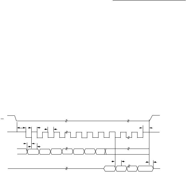
CDC CONVERSION TIME
The time required for one complete measurement by the CDC is defined as the CDC conversion time. For optimal system performance, configure the AD7142 CDC conversion time within a range of 35 ms to 40 ms. The SEQUENCE_STAGE_NUM, FF_SKIP_CNT, and DECIMATION registers determine the conversion time as listed in Table 8.
Rev. PrD | Page 13 of 64
AD7142/AD7142-1 |
|
|
|
Preliminary Technical Data |
|||
|
|
|
|
|
|
|
|
Table 8. CDC Conversion Times for Full Power Mode |
|
|
|
|
|
||
|
DECIMATION = 64 |
DECIMATION = 128 |
DECIMATION = 256 |
||||
|
|
|
|
|
|
|
|
SEQUENCE_STAGE_NUM |
|
CDC Conversion |
|
CDC Conversion |
|
CDC Conversion |
|
FF_SKIP_CNT |
Time (ms) |
FF_SKIP_CNT |
Time (ms) |
FF_SKIP_CNT |
Time (ms) |
||
0 |
11 |
9.2 |
11 |
18.4 |
|
11 |
36.5 |
1 |
11 |
18.4 |
11 |
36.8 |
|
5 |
36.5 |
2 |
11 |
27.6 |
7 |
36.8 |
|
3 |
36.5 |
3 |
11 |
36.8 |
5 |
36.8 |
|
2 |
36.5 |
4 |
9 |
38.4 |
4 |
38.4 |
|
2 |
46.0 |
5 |
7 |
36.8 |
3 |
36.8 |
|
1 |
36.8 |
6 |
6 |
37.6 |
2 |
32.2 |
|
1 |
43.0 |
7 |
5 |
36.8 |
2 |
36.8 |
|
1 |
49.1 |
8 |
4 |
34.5 |
2 |
41.4 |
|
0 |
27.6 |
9 |
4 |
38.4 |
1 |
30.7 |
|
0 |
30.7 |
10 |
3 |
33.8 |
1 |
33.8 |
|
0 |
33.7 |
11 |
3 |
36.8 |
1 |
36.8 |
|
0 |
36.8 |
|
|
|
|
|
|
|
|
For example, while operating with a decimation rate of 128, if the SEQUENCE_STAGE_NUM register is set to 5 for the conversion of six stages in a sequence, the FF_SKIP_CNT register should be set to 3 resulting in a conversion time of 36.8 ms. This example is shown in Figure 14.
Determining the FF_SKIP_CNT value is only required one time during the initial setup of the capacitance sensor interface. This value determines which CDC samples are not used (skipped) in the proximity detection fast FIFO.
Full Power Mode CDC Conversion Time
The full power mode CDC conversion time is set by configuring the SEQUENCE_STAGE_NUM, FF_SKIP_CNT and DECIMATION registers as outlined in Table 8.
Figure 16 shows a simplified timing diagram of the full power CDC conversion time. The full power mode CDC conversion time tCONV_FP is set using Table 8.
|
|
tCONV_FP |
|
|
|
CDC |
|
CONVERSION |
|
CONVERSION CONVERSION |
|
CONVERSION |
|
N |
|
N + 1 |
N + 2 |
|
|
|
|
|
05702-015 |
|
NOTES |
|
|
||
|
1. tCONV_FP = VALUE SET FROM TABLE 8. |
||||
Figure 16. Full Power Mode CDC Conversion Time
Low Power Mode CDC Conversion Time with Delay
The frequency of each CDC conversion while operating in the low power automatic wake up mode is controlled by using the LP_CONV_DELAY register bits (Bits[3:2] in Register 0x00), in addition to the registers listed in Table 8. This feature provides some flexibility for optimizing the conversion time to meet system requirements vs. AD7142 power consumption. For example, maximum power savings is achieved when the
LP_CONV_DELAY is set to 3. With a setting of 3, the AD7142 automatically wakes up, performing a conversion every 400 ms.
Table 9. LP_CONV_DELAY Settings
LP_CONV_DELAY BITS |
Delay Between Conversions |
|
|
00 |
100 ms |
01 |
200 ms |
10 |
300 ms |
11 |
400 ms |
Figure 17 shows a simplified timing example of the low power CDC conversion time. As shown, the low power CDC conversion time is set by tCONV_FP and the LP_CONV_DELAY register.
CDC |
|
|
tCONV_LP |
|
|
|
|
|
CONVERSION N |
|
CONVERSION N + 1 |
|
|
CONVERSION |
|
|
|
|
||
|
|
|
|
|
|
|
|
|
|
|
05702-016 |
||
|
1. tCONV_LP = tCONV_FP + LP_CONV_DELAY |
|||||
|
NOTES |
|
|
|
||
Figure 17. Low Power Mode CDC Conversion Time CDC Conversion Results
CDC CONVERSION RESULTS
Certain applications, such as a slider function, require reading back the CDC conversion results for host processing. The registers required for host processing are located in Register Bank 3. The host processes the data read back from these registers to determine relative position information.
In addition to the results registers in Bank 3, the AD7142 provides the 16-bit CDC output data directly starting at Address 0x00B of Register Bank 1. Reading back the CDC 16-bit conversion data register allows for customer specific application data processing.
Rev. PrD | Page 14 of 64

Preliminary Technical Data |
AD7142/AD7142-1 |
|
|
NON-CONTACT PROXIMITY DETECTION
The AD7142 internal signal processing continuously monitors all capacitance sensors for non-contact proximity detection. This feature provides the ability to detect when a user is approaching a sensor, at which time all internal calibration is immediately disabled while the AD7142 is automatically configured to detect a valid contact.
The proximity control register bits are described in Table 10. The FP_PROXIMITY_CNT and LP_PROXIMITY_CNT register bits control how long the calibration disable period is after proximity is detected. The calibration is disabled during this time and enabled again at the end of this period provided that the user is no longer approaching, or in contact with, the sensor. Figure 18 and Figure 19 show examples of how these registers are used to set the full and low power mode calibration disable periods.
Recalibration
In the event of a very long proximity detection event, such as a user hovering over a sensor for a long period of time, the FP_PROXIMITY_RECAL and LP_PROXIMITY_RECAL bits in register 0x004 can be applied to force a recalibration. This feature ensures that the ambient values are recalibrated regardless of how long the user may be hovering over a sensor. A recalibration ensures maximum AD7142 sensor performance. Figure 20 and Figure 21 show examples of using the FP_PROXIMITY_RECAL and LP_PROXIMITY_RECAL
Table 10. Proximity Control Registers (Refer to Figure 22)
register bits to force a recalibration while operating in the full and low power modes. These figures show a user approaching a sensor followed by the user leaving the sensor while the proximity detection remained active after the user left the sensor. This situation could occur if the user interaction created some moisture on the sensor for example thus causing the new sensor value to be different from the expected value. In this case, the internal recalibration would be applied to automatically recalibrate the sensor. The force calibration event takes two interrupt cycles: nothing should be read from or written to the AD7142 during the recalibration period.
Proximity Sensitivity
There are two conditions that set the internal proximity detection signal as described in Figure 22 with Comparator 1 and Comparator 2. Comparator 1 detects when a user is approaching a sensor. The sensitivity of Comparator 1 is controlled by PROXIMITY_DETECTION_RATE. For example, if PROXIMITY_DETECTION_RATE is set to 4, the Proximity 1 signal is set when the absolute difference between WORD1 and WORD3 exceed four LSB codes. Comparator 2 detects when a user is hovering over a sensor or approaches a sensor very slowly. The sensitivity of Comparator 2 is controlled by the PROXIMITY_RECAL_LVL in Register 0x003. For example, if PROXIMITY_RECAL_LVL is set to 75, the Proximity 2 signal is set when the absolute difference between the fast filter average value and the ambient value exceeds 75 LSB codes.
|
Length |
|
|
Register |
(Bits) |
Register Address |
Description |
FP_PROXIMITY_CNT |
4 |
0x002 |
Full power mode proximity control |
LP_PROXIMITY_CNT |
4 |
0x002 |
Low power mode proximity control |
FP_PROXIMITY_RECAL |
8 |
0x004 |
Full power mode proximity recalibration control |
LP_PROXIMITY_RECAL |
6 |
0x004 |
Low power mode proximity recalibration control |
PROXIMITY_RECAL_LVL |
8 |
0x003 |
Proximity recalibration level |
PROXIMITY_DETECTION_RATE |
6 |
0x003 |
Proximity detection rate |
|
|
USER APPROCHES |
|
USER LEAVES SENSOR |
|
|
|
|
|
|
|
|
|
|
|
|
|
|
|
|
|
|
|
|
|
|
|
|
|||||||||||||||||||
|
|
|
SENSOR HERE |
|
|
|
AREA HERE |
|
|
|
|
|
|
|
|
|
|
|
|
|
|
|
|
|
|
|
|
|
|
|
|
||||||||||||||||
CDC CONVERSIONS |
|
|
|
|
|
1 |
2 |
3 |
4 |
5 |
6 |
7 |
8 |
9 |
|
10 |
11 |
1213 14 15 |
16 |
|
|
|
|
|
|
|
|
|
|
|
|
|
|
|
|
|
|
|
tCONV_FP |
||||||||
|
|
|
|
|
|
|
|
|
|
|
|
|
|
|
|
|
|
|
|
|
|
|
|
|
|||||||||||||||||||||||
|
|
|
|
|
|
|
|
|
|
|
|
|
|
|
|
|
|
|
|
|
|
|
|
|
|||||||||||||||||||||||
|
|
|
|
|
|
|
|
|
|
|
|
|
|
|
|
|
|
|
|
|
|
|
|
|
|
|
|
|
|
||||||||||||||||||
(INTERNAL) |
|
|
|
|
|
|
|
|
|
|
|
|
|
|
|
|
|
|
|
|
|
|
|
|
|
|
|
|
|
|
|
|
|
|
|
|
|
|
|
|
|
|
|
|
|
|
|
|
|
|
|
|
|
|
|
|
|
|
|
|
|
|
|
|
|
|
|
|
|
|
|
|
|
|
|
|
|
|
|
|
|
|
|
|
|
|
|
|
|
|
|
|
|
|
|
|
|
|
|
|
|
|
|
|
|
|
tCALDIS |
|
|
|
|
|
|
|
|
|
|
|
|
|
|
|
|
|
|
|
|
|
|
|
|
|
|||||||||||
PROXIMITY DETECTION |
|
|
|
|
|
|
|
|
|
|
|
|
|
|
|
|
|
|
|
|
|
|
|
|
|
|
|
|
|
|
|
|
|
|
|
|
|||||||||||
|
|
|
|
|
|
|
|
|
|
|
|
|
|
|
|
|
|
|
|
|
|
|
|
|
|
|
|
|
|
|
|
|
|
|
|||||||||||||
|
|
|
|
|
|
|
|
|
|
|
|
|
|
|
|
|
|
|
|
|
|
|
|
|
|
|
|
|
|
|
|
|
|
|
|
|
|
|
|
|
|
|
|
|
|
|
|
(INTERNAL) |
|
|
|
|
|
|
|
|
|
|
|
|
|
|
|
|
|
|
|
|
|
|
|
|
|
|
|
|
|
|
|
|
|
|
|
|
|
|
|
|
|
|
|
|
|
|
|
CALIBRATION |
|
|
|
|
|
|
|
|
CALIBRATION DISABLED |
|
|
|
|
|
|
|
|
CALIBRATION ENABLED |
|||||||||||||||||||||||||||||
(INTERNAL) |
|
|
|
|
|
|
|
|
|
|
|
|
|
|
|
|
|
|
|
|
|
|
|
|
|
|
|
|
|
|
|
|
|
|
|
|
|
|
|
|
|
|
|
|
|
|
|
|
|
|
|
|
|
|
|
|
|
|
|
|
|
|
|
|
|
|
|
|
|
|
|
|
|
|
|
|
|
|
|
|
|
|
|
|
|
|
|
|
|
|
|
|
|
|
|
Figure 18. Full Power Mode Proximity Detection Example with FP_PROXIMITY = 1
05702-017
Rev. PrD | Page 15 of 64

AD7142/AD7142-1 |
Preliminary Technical Data |
|
|
|
|
USER APPROCHES |
|
USER LEAVES SENSOR |
|
|
|
|
|
|
|
|
|
|
|
|
|
|
|
|
|
|
|
|
|
|
|
|
|||||||||||||||||||
|
|
|
SENSOR HERE |
|
|
|
AREA HERE |
|
|
|
|
|
|
|
|
|
|
|
|
|
|
|
|
|
|
|
|
|
|
|
|
||||||||||||||||
CDC CONVERSIONS |
|
|
|
|
|
1 |
2 |
3 |
4 |
5 |
6 |
7 |
8 |
9 |
|
10 |
11 |
1213 14 15 |
16 |
|
|
|
|
|
|
|
|
|
|
|
|
|
|
|
|
|
|
|
tCONV_FP |
||||||||
|
|
|
|
|
|
|
|
|
|
|
|
|
|
|
|
|
|
|
|
|
|
|
|
|
|||||||||||||||||||||||
|
|
|
|
|
|
|
|
|
|
|
|
|
|
|
|
|
|
|
|
|
|
|
|
|
|||||||||||||||||||||||
|
|
|
|
|
|
|
|
|
|
|
|
|
|
|
|
|
|
|
|
|
|
|
|
|
|
|
|
|
|
||||||||||||||||||
(INTERNAL) |
|
|
|
|
|
|
|
|
|
|
|
|
|
|
|
|
|
|
|
|
|
|
|
|
|
|
|
|
|
|
|
|
|
|
|
|
|
|
|
|
|
|
|
|
|
|
|
|
|
|
|
|
|
|
|
|
|
|
|
|
|
|
|
|
|
|
|
|
|
|
|
|
|
|
|
|
|
|
|
|
|
|
|
|
|
|
|
|
|
|
|
|
|
|
|
|
|
|
|
|
|
|
|
|
|
|
tCALDIS |
|
|
|
|
|
|
|
|
|
|
|
|
|
|
|
|
|
|
|
|
|
|
|
|
|
|||||||||||
PROXIMITY DETECTION |
|
|
|
|
|
|
|
|
|
|
|
|
|
|
|
|
|
|
|
|
|
|
|
|
|
|
|
|
|
|
|
|
|
|
|
|
|||||||||||
|
|
|
|
|
|
|
|
|
|
|
|
|
|
|
|
|
|
|
|
|
|
|
|
|
|
|
|
|
|
|
|
|
|
|
|||||||||||||
|
|
|
|
|
|
|
|
|
|
|
|
|
|
|
|
|
|
|
|
|
|
|
|
|
|
|
|
|
|
|
|
|
|
|
|
|
|
|
|
|
|
|
|
|
|
|
|
(INTERNAL) |
|
|
|
|
|
|
|
|
|
|
|
|
|
|
|
|
|
|
|
|
|
|
|
|
|
|
|
|
|
|
|
|
|
|
|
|
|
|
|
|
|
|
|
|
|
|
|
CALIBRATION |
|
|
|
|
|
|
|
|
CALIBRATION DISABLED |
|
|
|
|
|
|
|
|
CALIBRATION ENABLED |
|||||||||||||||||||||||||||||
(INTERNAL) |
|
|
|
|
|
|
|
|
|
|
|
|
|
|
|
|
|
|
|
|
|
|
|
|
|
|
|
|
|
|
|
|
|
|
|
|
|
|
|
|
|
|
|
|
|
|
|
|
|
|
|
|
|
|
|
|
|
|
|
|
|
|
|
|
|
|
|
|
|
|
|
|
|
|
|
|
|
|
|
|
|
|
|
|
|
|
|
|
|
|
|
|
|
|
|
NOTES
1.CONVERSION TIME tCONV_LP = (tCONV_FP + LP_CONV_DELAY).
2.PROXIMITY IS SET WHEN USER APPROACHES THE SENSOR AT WHICH TIME THE INTERNAL CALIBRATION IS DISABLED.
3.tCALDIS = (tCONV_LP × LP_PROXIMITY_CNT × 4) + LP_CONV_DELAY.
Figure 19. Low Power Mode Proximity Detection with LP_PROXIMITY = 4 and LP_CONV_DELAY = 0
05702-018
USER APPROCHES |
USER LEAVES SENSOR |
SENSOR HERE |
AREA HERE |
|
|
|
|
|
|
|
|
|
|
|
|
|
USER IN CONTACT WITH SENSOR |
|
|
|
|
|
|
|
CDC CONVERSION VALUES EXCEED |
|
|
||||||||||||||||||||||||||||||||||||||||||||||||||||||||||||||||||||
|
|
|
|
|
|
|
|
|
|
|
|
|
|
|
|
|
|
|
|
|
|||||||||||||||||||||||||||||||||||||||||||||||||||||||||||||||||||||||
|
|
|
|
|
|
|
|
|
|
|
|
|
|
|
|
|
|
|
|
PROXIMITY_RECALIBRATION _LVL |
|
|
|||||||||||||||||||||||||||||||||||||||||||||||||||||||||||||||||||||
|
|
|
|
|
|
|
|
|
|
|
16 |
|
|
|
|
|
|
|
|
|
|
30 |
|
|
|
|
|
|
|
|
|
|
|
|
|
|
|
|
|
|
|
|
|
|
|
|
|
|
|
|
|
|
|
70 |
|
|
|
|
|
|
|
|
|
|
|
|
tCONV_FP |
||||||||||||||||||||||||
|
|
|
|
|
|
|
|
|
|
|
|
|
|
|
|
|
|
|
|
|
|
|
|
|
|
|
|
|
|
|
|
|
|
|
|
|
|
|
|
|
|
|
|
|
|
|
|
|
|
|
|
|
|
|
|
|
|
|
|
|
|
|
|
||||||||||||||||||||||||||||
|
|
|
|
|
|
|
|
|
|
|
|
|
|
|
|
|
|
|
|
|
|
|
|
|
|
||||||||||||||||||||||||||||||||||||||||||||||||||||||||||||||||||
CDC CONVERSIONS |
|
|
|
|
|
|
|
|
|
|
|
|
|
|
|
|
|
|
|
|
|
|
|
|
|
|
|
|
|
|
|
|
|
|
|
|
|
|
|
|
|
|
|
|
|
|
|
|
|
|
|
|
|
|
|
|
|
|
|
|
|
|
|
|
|
|
|
|
|
|
|
|
|
|
|
|
|
|
|
|
|
|
|
|
|
|
|
|
|
||
(INTERNAL) |
|
|
|
|
|
|
|
|
|
|
|
|
|
|
|
|
|
|
|
|
|
|
|
|
|
|
|
|
|
|
|
|
|
|
|
|
|
|
|
|
|
|
|
|
|
|
|
|
|
|
|
|
|
|
|
|
|
|
|
|
|
|
|
|
|
|
|
|
|
|
|
|
|
|
|
|
|
|
|
|
|
|
|
|
|
|
|
|
|
|
|
|
|
|
|
|
|
|
|
|
|
|
|
|
|
|
|
|
tDISCAL |
|
|
|
|
|
|
|
|
|
|
|
|
|
|
|
|
|
|
|
|
|
|
|
|
|
|
|
|
|
|
|
|
|
|
|
|
|
|
|
|
|
|
|
|
|
|
|
|
|
|
|
|
|
|
|
|
|
|
|
|
|
|
|
|
|
|||||||||
|
|
|
|
|
|
|
|
|
|
|
|
|
|
|
|
|
|
|
|
|
|
|
|
|
|
|
|
|
|
|
|
|
|
|
|
|
|
|
|
|
|
|
|
|
|
|
|
|
|
|
|
|
|
|
|
|
|
|
|
|
|
|
|
|
|
|
|
|
|
|
|
|
|
|
|
|
|
|
|
|
|
||||||||||
PROXIMITY DETECTION (INTERNAL)
CALIBRATION |
CALIBRATION DISABLED |
RECALIBRATION PERIOD |
CALIBRATION ENABLED |
|
(INTERNAL) |
||||
|
|
|
||
RECALIBRATION |
|
tRECAL |
|
|
|
|
|
||
(INTERNAL) |
|
|
|
NOTES
1.CONVERSION TIME tCONV_FP DETERMINED FROM TABLE 8
2.tDISCAL = tCONV_FP × FP_PROXIMITY_CNT)
3.tRECAL = (tCONV_FP × FP_PROXIMITY_RECAL)
Figure 20. Full Power Mode Proximity Detection with Forced Recalibration Example with FP_PROXIMITY = 1 and FP_PROXIMITY_RECAL = 40
05702-019
Rev. PrD | Page 16 of 64
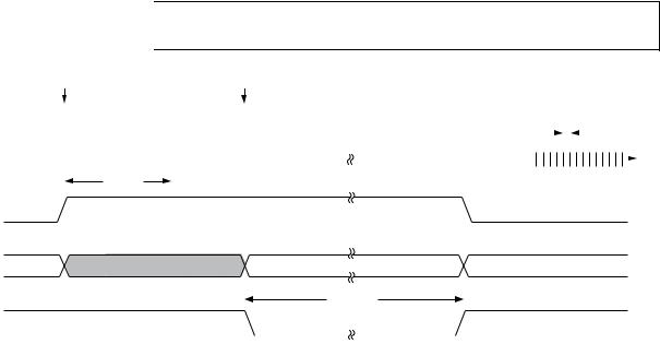
Preliminary Technical Data |
AD7142/AD7142-1 |
|
|
USER APPROCHES |
USER LEAVES SENSOR |
SENSOR HERE |
AREA HERE |
|
|
|
|
|
|
|
|
|
|
|
|
|
|
USER IN CONTACT WITH SENSOR |
|
|
|
|
|
|
CDC CONVERSION VALUES EXCEED |
|
|
|
|
|
|
|
|
|
|
|
|
|
|
|
|
|
|
|
||||||||||||||||||||||||||||||||||||||||||||||||||||
|
|
|
|
|
|
|
|
|
|
|
|
|
|
|
|
|
|
|
|
|
|
|
|
|
|
|
|
|
|
|
|
|
|
|
|
|
|
|
||||||||||||||||||||||||||||||||||||||||||||||||||||||
|
|
|
|
|
|
|
|
|
|
|
|
|
|
|
|
|
|
|
PROXIMITY_RECALIBRATION _LVL |
|
|
|
|
|
|
|
|
|
|
|
|
|
|
|
|
|
tCONV_FP |
|||||||||||||||||||||||||||||||||||||||||||||||||||||||
CDC CONVERSIONS |
|
|
|
|
|
|
|
|
|
|
|
16 |
|
|
|
|
|
|
|
|
|
|
|
|
30 |
|
|
|
|
|
|
|
|
|
|
|
|
|
|
|
|
|
|
|
|
|
|
|
|
|
|
|
|
|
|
70 |
|
|
|
|
|
|
|
|
|
|
|
|
||||||||||||||||||||||||
|
|
|
|
|
|
|
|
|
|
|
|
|
|
|
|
|
|
|
|
|
|
|
|
|
|
|
|
|
|
|
|
|
|
|
|
|
|
|
|
|
|
|
|
|
|
|
|
|
|
|
|
|
|
|
|
|
|
|
|
|
|
|
|
|
||||||||||||||||||||||||||||
|
|
|
|
|
|
|
|
|
|
|
|
|
|
|
|
|
|
|
|
|
|
|
|
|
|
|
|
|
|
|
|
|
|
|
|
|
|
|
|
|
|
|
|
|
|
|
|
|
|
|
|
|
|
|
|
|
|
|
|
|
|
|
|
|
|
|
||||||||||||||||||||||||||
|
|
|
|
|
|
|
|
|
|
|
|
|
|
|
|
|
|
|
|
|
|
|
|
|
|
|
|
|
|
|
|
|
|
|
|
|
|
|
|
|
|
|
|
|
|
|
|
|
|
|
|
|
|
|
|
|
|
|
|
|
|
|
|
|
|
|
|
|
|
|
|
|
|
|
|
|
|
|
|
|
|
|
|
|
|
|
|
|
|
|
||
(INTERNAL) |
|
|
|
|
|
|
|
|
|
|
|
|
|
|
|
|
|
|
|
|
|
|
|
|
|
|
|
|
|
|
|
|
|
|
|
|
|
|
|
|
|
|
|
|
|
|
|
|
|
|
|
|
|
|
|
|
|
|
|
|
|
|
|
|
|
|
|
|
|
|
|
|
|
|
|
|
|
|
|
|
|
|
|
|
|
|
|
|
|
|
|
|
PROXIMITY DETECTION |
|
|
|
|
|
|
tDISCAL |
|
|
|
|
|
|
|
|
|
|
|
|
|
|
|
|
|
|
|
|
|
|
|
|
|
|
|
|
|
|
|
|
|
|
|
|
|
|
|
|
|
|
|
|
|
|
|
|
|
|
|
|
|
|
|
|
|
|
|
|
|
|
|
|
|
||||||||||||||||||||
|
|
|
|
|
|
|
|
|
|
|
|
|
|
|
|
|
|
|
|
|
|
|
|
|
|
|
|
|
|
|
|
|
|
|
|
|
|
|
|
|
|
|
|
|
|
|
|
|
|
|
|
|
|
|
|
|
|
|
|
|
|
|
|
|
|
|
|
|
|
|
||||||||||||||||||||||
|
|
|
|
|
|
|
|
|
|
|
|
|
|
|
|
|
|
|
|
|
|
|
|
|
|
|
|
|
|
|
|
|
|
|
|
|
|
|
|
|
|
|
|
|
|
|
|
|
|
|
|
|
|
|
|
|
|
|
|
|
|
|
|
|
|
|
|
|
|
|
|
|
|
|
|
|
|
|
|
|
||||||||||||
(INTERNAL) |
|
|
|
|
|
|
|
|
|
|
|
|
|
|
|
|
|
|
|
|
|
|
|
|
|
|
|
|
|
|
|
|
|
|
|
|
|
|
|
|
|
|
|
|
|
|
|
|
|
|
|
|
|
|
|
|
|
|
|
|
|
|
|
|
|
|
|
|
|
|
|
|
|
|
|
|
|
|
|
|
|
|||||||||||
CALIBRATION |
|
|
|
|
|
CALIBRATION DISABLED |
|
|
|
|
|
|
|
|
|
RECALIBRATION PERIOD |
|
|
|
|
|
|
|
CALIBRATION ENABLED |
||||||||||||||||||||||||||||||||||||||||||||||||||||||||||||||||||||
(INTERNAL) |
|
|
|
|
|
|
|
|
|
|
|
|
|
|
|
|
|
|
|
|
|
|||||||||||||||||||||||||||||||||||||||||||||||||||||||||||||||||||||||
|
|
|
|
|
|
|
|
|
|
|
|
|
|
|
|
|
|
|
|
|
|
|
|
|
|
|
|
|
|
|
|
|
|
|
|
|
|
|
|
|
|
|
|
|
|
|
|
|
|
|
|
|
|
|
|
|
|
|
|
|
|
|
|
|
|
|
|
|
|
|
|
|
|
|
|
|
|
|
|
|
||||||||||||
|
|
|
|
|
|
|
|
|
|
|
|
|
|
|
|
|
|
|
|
|
|
|
|
|
|
|
|
|
|
|
|
|
|
|
|
|
|
|
|
|
|
|
|
|
|
|
|
|
|
|
|
|
|
|
tRECAL |
|
|
|
|
|
|
|
|
|
|
|
|
|
|
|
|
|
|
|
||||||||||||||||||
RECALIBRATION |
|
|
|
|
|
|
|
|
|
|
|
|
|
|
|
|
|
|
|
|
|
|
|
|
|
|
|
|
|
|
|
|
|
|
|
|
|
|
|
|
|
|
|
|
|
|
|
|
|
|
|
|
|
|
|
|
|
|
|
|
|
|
|
|
|
|
|
|
|
|
|
|
|
|
|
|
|
|
|
|
||||||||||||
(INTERNAL) |
|
|
|
|
|
|
|
|
|
|
|
|
|
|
|
|
|
|
|
|
|
|
|
|
|
|
|
|
|
|
|
|
|
|
|
|
|
|
|
|
|
|
|
|
|
|
|
|
|
|
|
|
|
|
|
|
|
|
|
|
|
|
|
|
|
|
|
|
|
|
|
|
|
|
|
|
|
|
|
|
||||||||||||
|
|
|
|
|
|
|
|
|
|
|
|
|
|
|
|
|
|
|
|
|
|
|
|
|
|
|
|
|
|
|
|
|
|
|
|
|
|
|
|
|
|
|
|
|
|
|
|
|
|
|
|
|
|
|
|
|
|
|
|
|
|
|
|
|
|
|
|
|
|
|
|
|
|
|
|
|
|
|
|
|
|
|
|
|
|
|
|
|
|
|
|
|
NOTES
1.CONVERSION TIME tCONV_LP = tCONV_HP + LP_CONV_DELAY.
2.tDISCAL = tCONV_LP × (16 × LP_PROXIMITY_CNT)
3.tRECAL = (tCONV_LP × LP_PROXIMITY_RECAL × 4)
Figure 21. Low Power Mode Proximity Detection with Forced Recalibration Example with LP_PROXIMITY = 4 and LP_PROXIMITY_RECAL = 10
05702-020
Rev. PrD | Page 17 of 64
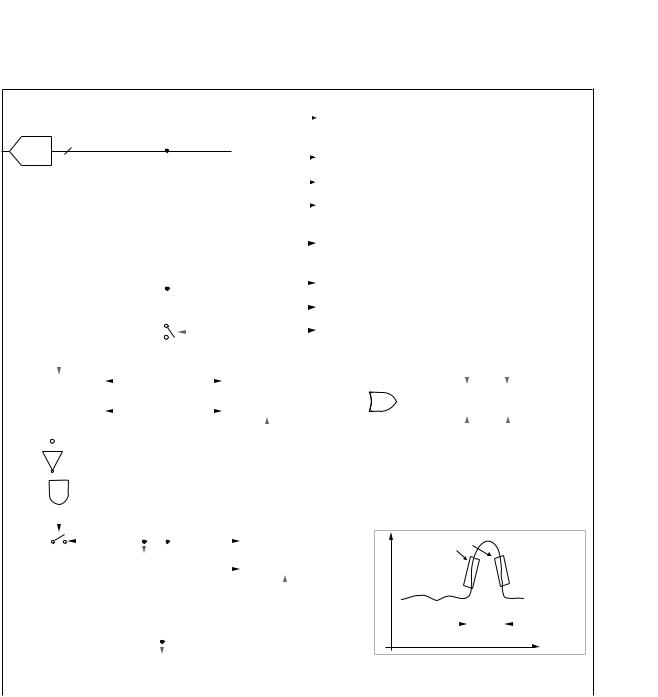
AD7142/AD7142-1 |
Preliminary Technical Data |
|
|
|
|
|
|
|
|
|
|
|
|
|
|
|
|
|
|
|
|
|
|
|
|
|
|
|
|
|
|
|
|
|
|
|
|
|
|
|
|
|
|
|
|
STAGE_MAX_WORD0 |
|
|
|
|
|
|
|
|
|
|
|
|
|
|
|
|
|
|
|
|
||||
|
|
|
|
|
|
|
|
|
|
|
|
|
|
|
|
|
|
|
|
|
|
|
|
|
|
|
|
|
|
|
|
|
|
|
|
|
|
|
|
|
|
STAGE_MAX_WORD1 |
|
|
BANK 3 REGISTERS |
|
|
|
|
|
|
|
|
|
||||||||||||
|
|
|
|
|
|
|
|
|
|
|
|
|
|
|
|
|
|
|
|
|
|
|
|
|
|
|
|
|
|
|
|
|
|
|
|
|
|
|
|
|
|
|
|
|
|
|
|
|
|
|
|
|
||||||||||||||
|
|
|
|
|
|
|
|
|
|
|
|
|
|
|
|
|
|
|
|
|
|
|
|
|
|
|
|
|
|
|
|
|
|
|
|
|
|
|
|
|
|
STAGE_MAX_WORD2 |
|
|
|
|
|
|
|
|
|
|
|
|||||||||||||
|
|
|
|
|
|
|
|
|
|
|
|
|
|
|
|
|
|
|
|
|
|
|
|
|
|
|
|
|
|
|
|
|
|
|
|
|
|
|
|
|
|
|
|
|
|
|
|
|
|
|
|
|
|
|
|
|
|
|
|
|
|
|||||
|
|
|
Σ- |
16 |
|
|
|
|
|
|
|
|
|
|
|
|
|
|
|
|
|
|
|
|
|
|
|
|
|
|
|
|
|
|
|
|
|
|
STAGE_MAX_WORD3 |
|
|
|
|
|
|
|
|
|
|
|
|
|
|
|
|
|
|
|
|
|||||||
|
|
|
|
|
|
|
|
|
|
|
|
|
|
|
|
|
|
|
|
|
|
|
|
|
|
|
|
|
|
|
|
|
|
|
|
|
|
|
|
|
|
|
|
|
|
|
|
|
|
|
|
|
|
|
|
|
|
|
|
|
|
|||||
|
|
16-BIT |
|
|
|
|
|
|
|
|
|
|
|
|
|
|
|
|
|
|
|
|
|
|
|
|
MAX LEVEL |
|
|
|
|
|
|
|
|
STAGE_MAX_AVG |
|
|
|
|
|
|
|
|
|
|
|
|
|
|
|
|
|
|
|
|
||||||||||
|
|
|
CDC |
|
|
|
|
|
|
|
|
|
|
|
|
|
|
|
|
|
|
|
|
|
|
|
|
|
|
|
|
|
|
|
|
|
|
|
|
|
|
|
|
|
|
|
|
|
|
|
|
|
|
|
|
|||||||||||
|
|
|
|
|
|
|
|
|
|
|
|
|
|
|
|
|
|
|
|
|
|
|
|
|
|
|
DETECTION |
|
|
|
|
|
|
|
|
BANK 3 REGISTERS |
|
|
|
|
|
|
|
|
|
|
|
|
|
|
|
|
|
|
|
|
||||||||||
|
|
|
|
|
|
|
|
|
|
|
|
|
|
|
|
|
|
|
|
|
|
|
|
|
|
|
|
|
|
|
|
|
|
|
|
|
|
|
|
|
|
|
|
|
|
|
|
|
|
|
|
|
|
|
|
|
|
|||||||||
|
|
|
|
|
|
|
|
|
|
|
|
|
|
|
|
|
|
|
|
|
|
|
|
|
|
|
|
|
|
|
LOGIC |
|
|
|
|
|
|
|
|
|
|
|
|
|
|
|
|
|
|
|
|
|
|
|
|
|
|
|
|
|
|
|
|
|
||
|
|
|
|
|
|
|
|
|
|
|
|
|
|
|
|
|
|
|
|
|
|
|
|
|
|
|
|
|
|
|
|
|
|
|
|
|
|
|
|
|
|
STAGE_MAX_TEMP |
|
|
|
|
|
|
|
|
|
|
|
|
|
|
|
|
|
|
|
|
||||
|
|
|
|
|
|
|
|
|
|
|
|
|
|
|
|
|
|
|
|
|
|
|
|
|
|
|
|
|
|
|
|
|
|
|
|
|
|
|
|
|
|
BANK 3 REGISTERS |
|
|
|
|
|
|
|
|
|
|
|
|
|
|
|
|
|
|
|
|
||||
|
|
|
|
|
|
|
|
|
|
|
|
|
|
|
|
|
|
|
|
|
|
|
|
|
|
|
|
|
|
|
|
|
|
|
|
|
|
|
|
|
|
|
|
|
|
|
|
|
|
|
|
|
|
|
|
|
|
|
|
|
|
|
|
|
|
|
|
|
|
|
|
|
|
|
|
|
|
|
|
|
|
|
|
|
|
|
|
|
|
|
|
|
|
|
|
|
|
|
|
|
|
|
|
|
|
STAGE_HIGH_THRESHOLD |
|
|
|
|
|
|
|
|
|
|
|
|
|
|
|
|
|
|
|||||||||
|
|
|
|
|
|
|
|
|
|
|
|
|
|
|
|
|
|
|
|
|
|
|
|
|
|
|
|
|
|
|
|
|
|
|
|
|
|
|
|
|
|
BANK 3 REGISTERS |
|
|
|
|
|
|
|
|
|
|
|
|
|
|
|
|
|
|
|
|
||||
|
|
|
|
|
|
|
|
|
|
|
|
|
|
|
|
|
|
|
|
|
|
|
|
|
|
|
|
|
|
|
|
|
|
|
|
|
|
|
|
|
|
|
|
|
|
|
|
|
|
|
|
|
|
|
|
|
|
|
|
|
|
|||||
|
|
|
|
|
|
|
|
|
|
|
|
|
|
|
|
|
|
|
|
|
|
|
|
|
|
|
|
|
|
|
|
|
|
|
|
|
|
|
|
|
|
|
|
|
|
|
|
|
|
|
|
|
|
|
|
|
|
|
|
|
|
|||||
|
|
|
|
|
|
|
|
|
|
|
|
|
|
|
|
|
|
|
|
|
|
|
|
|
|
|
|
|
|
|
|
|
|
|
|
|
|
|
|
|
STAGE_MIN_WORD0 |
|
|
|
|
|
|
|
|
|
|
|
|
|
|
|
|
|
|
|
|
|||||
|
|
|
|
|
|
|
|
|
|
|
|
|
|
|
|
|
|
|
|
|
|
|
|
|
|
|
|
|
|
|
|
|
|
|
|
|
|
|
|
|
STAGE_MIN_WORD1 |
|
|
BANK 3 REGISTERS |
|
|
|
|
|
|
|
|
|
|||||||||||||
|
|
|
|
|
|
|
|
|
|
|
|
|
|
|
|
|
|
|
|
|
|
|
|
|
|
|
|
|
|
|
|
|
|
|
|
|
|
|
|
|
|
|
|
|
|
|
|
|
|
|
|
|||||||||||||||
|
|
|
|
|
|
|
|
|
|
|
|
|
|
|
|
|
|
|
|
|
|
|
|
|
|
|
|
|
|
|
|
|
|
|
|
|
|
|
|
|
STAGE_MIN_WORD2 |
|
|
|
|
|
|
|
|
|
|
|
||||||||||||||
|
|
|
|
|
|
|
|
|
|
|
|
|
|
|
|
|
|
|
|
|
|
|
|
|
|
|
|
|
|
|
|
|
|
|
|
|
|
|
|
|
|
|
|
|
|
|
|
|
|
|
|
|
|
|
|
|
|
|
|
|
||||||
|
|
|
|
|
|
|
|
|
|
|
|
|
|
|
|
|
|
|
|
|
|
|
|
|
|
|
|
|
|
|
|
|
|
|
|
|
|
|
|
|
STAGE_MIN_WORD3 |
|
|
|
|
|
|
|
|
|
|
|
|
|
|
|
|
|
|
|
|
|||||
|
|
|
|
|
|
|
|
|
|
|
|
|
|
|
|
|
|
|
|
|
|
|
|
|
|
|
|
|
|
MIN LEVEL |
|
|
|
|
|
|
|
|
|
|
|
|
|
|
|
|
|
|
|
|
|
|
|
|
|
|
|
|
|
|
||||||
|
|
|
|
|
|
|
|
|
|
|
|
|
|
|
|
|
|
|
|
|
|
|
|
|
|
|
|
|
|
|
|
|
|
|
|
|
|
STAGE_MIN_AVG |
|
|
|
|
|
|
|
|
|
|
|
|
|
|
|
|
|
|
|
|
|
|||||||
|
|
|
|
|
|
|
|
|
|
|
|
|
|
|
|
|
|
|
|
|
|
|
|
|
|
|
|
|
|
DETECTION |
|
|
|
|
|
|
|
|
BANK 3 REGISTER3 |
|
|
|
|
|
|
|
|
|
|
|
|
|
|
|
|
|
|
|
|
|||||||
|
|
|
|
|
|
|
|
|
|
|
|
|
|
|
|
|
|
|
|
|
|
|
|
|
|
|
|
|
|
|
|
|
|
|
|
|
|
|
|
|
|
|
|
|
|
|
|
|
|
|
|
|
|
|
||||||||||||
|
|
|
|
|
|
|
|
|
|
|
|
|
|
|
|
|
|
|
|
|
|
|
|
|
|
|
|
|
|
|
LOGIC |
|
|
|
|
|
|
|
|
|
|
|
|
|
|
|
|
|
|
|
|
|
|
|
|
|
|
|
|
|
|
|
|
|
||
|
|
|
|
|
|
|
|
|
|
|
|
|
|
|
|
|
|
|
|
|
|
|
|
|
|
|
|
|
|
|
|
|
|
|
|
|
|
|
|
|
|
|
|
|
|
|
|
|
|
|
|
|
|
|
|
|
|
|
|
|
||||||
|
|
|
|
|
|
|
|
|
|
|
|
|
|
|
|
|
|
|
|
|
CONTROL |
|
|
|
|
|
|
|
|
|
|
|
|
STAGE_MIN_TEMP |
|
|
|
|
|
|
|
|
|
|
|
|
|
|
|
|
|
|
|
|
||||||||||||
|
|
|
|
|
|
|
|
|
|
|
|
|
|
|
|
|
|
|
|
|
LOGIC |
|
|
|
|
|
|
|
|
|
|
|
|
|
|
|
|
BANK 3 REGISTERS |
|
|
|
|
|
|
|
|
|
|
|
|
|
|
|
|
|
|
|
|
||||||||
|
|
|
|
|
|
|
|
|
|
|
|
|
|
|
|
|
|
|
|
|
|
|
|
|
|
|
|
|
|
|
|
|
|
|
|
|
|
|
|
|
|
|
|
|
|
|
|
|
|
|
|
|
|
|
|
|
|
|
|
|
|
|
|
|
|
|
|
|
|
|
|
|
|
|
|
|
|
|
|
|
|
|
SW |
|
|
|
|
|
|
|
|
|
|
|
|
|
|
|
|
|
|
|
|
|
STAGE_LOW_THRESHOLD |
|
|
|
|
|
|
|
|
|
|
|
|
|
|
|
|
||||||||||||
|
|
|
|
|
|
|
|
|
|
|
|
|
|
|
|
|
|
|
|
|
|
|
|
|
|
|
|
|
|
|
|
|
|
|
|
|
|
|
|
BANK 3 REGISTERS |
|
|
|
|
|
|
|
|
|
|
|
|
|
|
|
|
|
|
|
|
||||||
|
|
|
|
|
|
|
|
|
|
|
|
|
|
|
|
|
|
|
|
|
|
|
|
|
|
|
|
|
|
|
|
|
|
|
|
|
|
|
|
|
|
|
|
|
|
|
|
|
|
|
|
|
|
|
|
|
|
|
|
|||||||
|
|
|
|
|
|
|
|
|
|
|
|
|
|
|
|
|
|
|
|
|
|
|
|
|
|
|
|
|
|
|
|
|
|
|
|
|
|
|
|
|
|
|
|
|
|
|
|
|
|
|
|
|
|
|
|
|
|
|
|
|
|
|||||
|
SLOW_FILTER_UPDATE_LVL |
|
|
|
|
|
|
|
|
|
|
|
|
|
|
|
|
|
|
|
|
|
|
|
|
|
|
|
|
|
|
|
|
|
FP_PROXIMITY_CNT |
|
|
LP_PROXIMITY_CNT |
|
|||||||||||||||||||||||||||
|
|
|
REGISTER 0x003 |
|
|
|
|
|
|
|
|
|
|
|
|
|
|
|
|
|
|
|
|
|
|
|
|
|
|
|
|
|
|
|
|
|
|
|
|
|||||||||||||||||||||||||||
|
|
|
|
|
|
|
|
|
|
|
|
|
|
|
|
|
|
|
|
|
|
|
|
|
|
|
|
|
|
|
|
|
|
|
|
|
REGISTER 0x004 |
|
|
|
|
REGISTER 0X004 |
|
|||||||||||||||||||||||
|
|
|
COMPARATOR 3 |
|
|
|
STAGE_FF_WORD0 |
|
|
|
|
|
|
COMPARATOR 1 |
|
PROXIMITY 1 |
|
|
|
|
|
|
|
|
|
|
|
|
|
|
|
|
|
|
|
|
|
|||||||||||||||||||||||||||||
|
|
|
|
|
|
|
|
|
|
|
|
|
|
|
|
|
|
|
|
|
|
|
|
|
|
|
|
|
|
|
|
|
||||||||||||||||||||||||||||||||||
|
|
|
WORD 0 – WORD 3 |
|
|
|
|
|
STAGE_FF_WORD1 |
|
|
|
|
|
|
WORD 0 – WORD 3 |
|
|
|
PROXIMITY |
|
PROXIMITY TIMING |
|
|
|
|
||||||||||||||||||||||||||||||||||||||||
|
|
|
|
|
|
|
|
STAGE_FF_WORD2 |
|
|
|
|
|
|
|
|
|
|
|
|
|
|
|
|
|
|
|
|
|
|||||||||||||||||||||||||||||||||||||
|
|
|
|
|
|
|
|
|
|
|
|
|
|
|
|
|
|
|
|
|
|
|
|
|
|
|
|
|
|
|
|
|
|
|
|
|
|
|
|
|
|
|
|
CONTROL LOGIC |
|
|
|
|
||||||||||||||||||
|
|
|
|
|
|
|
|
|
|
|
|
|
|
|
STAGE_FF_WORD3 |
|
|
|
|
|
|
|
|
|
|
|
|
|
|
|
|
|
|
|
|
|
|
|
|
|
|
|
|
|
|
|
|
|
|
|
|
|
|
|
|
|
|
|
||||||||
|
|
|
|
|
|
|
EN |
|
|
STAGE_FF_WORD4 |
|
|
|
|
|
|
|
|
|
|
|
|
|
|
|
|
|
|
|
|
|
|
|
|
|
|
|
|
|
|
|
|
|
|
|
|
|
|
|
|
|
|
|
|||||||||||||
|
|
PROXIMITY |
|
FILTER |
|
|
STAGE_FF_WORD5 |
|
|
PROXIMITY_DETECTION_RATE |
|
|
|
|
|
|
|
FP_PROXIMITY_RECAL |
|
|
LP_PROXIMITY_RECAL |
|
||||||||||||||||||||||||||||||||||||||||||||
|
|
|
|
|
|
|
|
|
STAGE_FF_WORD6 |
|
|
|
|
|
|
REGISTER 0x003 |
|
|
|
|
|
|
|
|
|
|
|
|
||||||||||||||||||||||||||||||||||||||
|
|
|
|
|
|
|
|
|
|
|
|
|
|
|
|
|
|
|
|
|
|
|
|
|
|
|
|
|
|
|
REGISTER 0x004 |
|
|
|
|
|
REGISTER 0X004 |
|
||||||||||||||||||||||||||||
|
|
|
|
|
|
|
|
|
|
|
|
|
|
|
|
|
|
|
|
|
|
|
|
|
|
|
|
|
|
|
|
|
|
|
|
|
||||||||||||||||||||||||||||||
|
|
|
|
|
|
|
SLOW |
|
|
STAGE_FF_WORD7 |
|
|
|
|
|
|
|
|
|
|
|
|
|
|
|
|
|
|
|
|
|
|
|
|
|
|
|
|
|
|
|
|
|
|
|
|
|
|
|
|
|
|
|
|||||||||||||
|
|
|
|
|
|
|
|
|
|
|
|
|
|
BANK 3 REGISTERS |
|
|
|
|
PROXIMITY 2 |
|
|
|
|
|
|
|
|
|
|
|
|
|
|
|
|
|
|
|
|
|
|
|
|
|||||||||||||||||||||||
|
|
|
|
|
|
|
|
|
|
|
|
|
|
|
|
|
|
|
|
|
|
|
|
|
|
|
|
|
|
|
|
|
|
|
|
|
|
|
|
|
|
|
|
|
|
|
|
|
|
|
|
|
|
|
|
|
|
|
||||||||
|
|
|
|
|
|
|
|
|
|
|
|
|
|
|
|
|
|
|
|
|
|
|
|
|
|
|
|
|
|
|
|
|
|
|
|
|
|
|
|
|
|
|
|
|
|
|
|
|
|
|
|
|
|
|
|
|
|
|
|
|
|
|
|
|||
|
|
|
|
|
|
|
|
|
|
|
|
|
|
|
|
|
Σ7 |
WORD(N) |
|
|
|
|
|
|
|
|
|
|
|
|
|
|
|
|
|
|
|
|
|
|
|
|
|
|
|
|
|
|
|
|
|
|
|
|
|
|
|
|||||||||
|
|
|
|
|
|
|
|
|
|
|
|
|
|
|
|
|
|
|
|
|
|
|
|
|
|
|
|
|
|
|
|
|
|
|
|
|
|
|
|
|
|
|
|
|
|
|
|
|
|
|
|
|
|
|
|
|
|
|
||||||||
|
|
|
|
|
|
|
|
|
|
|
|
|
|
|
|
|
N = 0 |
|
|
|
|
|
|
|
|
|
|
|
|
|
|
|
|
|
|
|
|
|
|
|
|
|
|
|
|
|
|
|
|
|
|
|
|
|
|
|
|
|
|
|
|
|||||
|
|
|
|
|
|
|
|
|
|
|
|
|
|
|
|
|
|
8 |
|
|
|
|
|
|
|
|
|
|
|
|
|
|
|
|
|
|
|
|
|
|
|
|
|
|
|
|
|
|
|
|
|
|
|
|
|
|
|
|
|
|
|
|
|
|
||
|
|
|
SW1 |
|
|
|
|
|
|
|
|
|
|
|
|
|
|
|
|
|
|
|
|
|
|
|
|
|
|
|
|
|
|
|
|
|
|
|
|
|
|
|
|
|
|
|
|
|
|
|
|
|
|
|
|
|
|
|
|
|
|
|
|
|
||
|
|
|
|
|
|
|
|
|
|
|
|
|
|
|
|
|
|
|
|
|
|
|
|
|
COMPARATOR 2 |
|
|
|
|
|
|
|
|
|
|
STAGE_FF_WORDX |
|
|
|
|
|
|
|
|
|
|||||||||||||||||||||
|
|
|
|
|
|
|
|
|
|
|
|
|
|
|
|
|
|
|
|
|
|
|
|
|
|
|
|
|
|
|
|
|
|
|
|
|
|
|
|
|
|
|
|
|
|
|
|
|
|
|||||||||||||||||
|
|
|
|
|
|
|
|
|
|
|
|
|
|
|
|
|
|
|
|
|
|
|
|
|
|
|
|
|
|
|
AVERAGE – AMBIENT |
|
|
|
|
|
|
|
|
|
|
|
|
|
|
|
|
|
||||||||||||||||||
|
|
|
|
|
|
|
|
|
|
|
|
|
|
STAGE_FF_AVG |
|
|
|
|
|
|
|
|
|
|
|
|
|
|
|
|
|
|
|
|
|
|
|
|
|
|
|
|
|
|
|
|
|
|
|
|
|
|
|
|
|
|
||||||||||
|
|
STAGE_SF_WORD0 |
|
|
BANK 3 REGISTERS |
|
|
|
|
|
|
|
|
|
|
|
|
|
|
|
|
|
|
|
|
CODE |
|
|
|
|
|
|
|
|
|
|
|
|
|
|
|
|
|
|
|
|
|
|||||||||||||||||||
|
|
STAGE_SF_WORD2 |
|
|
|
|
|
|
|
|
|
|
|
|
|
|
|
|
|
|
|
|
|
|
|
|
|
|
|
|
|
|
|
|
|
|
|
|
|
|
|
|
|
|
|
|
|
|
|
|
|
|
|
|
|
|
|
|
||||||||
|
|
STAGE_SF_WORD1 |
|
|
|
|
|
|
|
|
|
|
|
|
|
|
|
|
|
|
|
|
|
|
|
|
|
|
|
|
|
|
|
|
|
|
|
|
|
|
|
|
|
|
|
|
|
|
|
|
|
|
|
|
|
|
|
|
|
|
||||||
|
|
|
|
|
|
|
|
|
|
|
|
|
|
|
|
|
|
|
|
|
|
|
|
|
|
|
|
|
|
|
|
|
|
|
|
|
|
|
|
|
|
|
|
|
|
|
|
|
|
|
|
|
|
|
|
|
|
|
|
|
|
|
|
|
|
|
|
|
STAGE_SF_WORD3 |
|
|
|
|
|
|
|
|
|
|
|
|
|
|
|
|
|
|
|
|
|
|
PROXIMITY_RECAL_LVL |
|
|
|
OUTPUT |
|
|
|
|
|
|
|
|
|
|
|
|
|
|
|
|
AMBIENT VALUE |
|
|||||||||||||||||||
|
|
|
|
|
|
|
|
|
|
|
|
|
|
|
|
|
|
|
|
|
|
REGISTER 0x003 |
|
|
|
|
|
|
|
|
|
|
|
|
|
|
|
|
SENSOR |
|
|
|
|
|
||||||||||||||||||||||
|
|
STAGE_SF_WORD5 |
|
|
|
|
|
|
|
|
|
|
|
|
|
|
|
|
|
|
|
|
|
|
|
|
|
|
|
|
|
|
|
|
|
|
|
|
|
|
|
|
|
|
|
|
|
|
|
|||||||||||||||||
|
|
STAGE_SF_WORD4 |
|
|
|
|
|
|
|
|
|
|
|
|
|
|
|
|
|
|
|
|
|
|
|
|
|
|
|
|
|
|
|
|
|
|
|
|
|
STAGE_SF_WORDX |
|
|
|
|
|
|
|
|
|
|||||||||||||||||
|
|
|
|
|
|
|
|
|
|
|
|
|
|
|
|
|
|
|
|
|
|
|
|
|
|
|
|
|
|
|
|
|
|
|
|
|
|
|
|
|
|
|
|
|
|
|
|
|||||||||||||||||||
|
|
|
|
|
|
|
|
|
|
|
|
|
|
|
|
|
|
|
|
|
|
|
|
|
|
|
|
|
|
|
|
|
|
|
|
|
|
|
|
|
|
|
|
CDC |
|
|
|
|
|
|
|
|
|
CONTACT |
|
|
|
|
|
|
|
|
||||
|
|
|
|
|
|
|
|
|
|
|
|
|
|
|
|
|
|
|
|
|
|
|
|
|
|
|
|
|
|
|
|
|
|
|
|
|
|
|
|
|
|
|
|
|
|
|
|
|
|
|
|
|
|
|
|
|
|
|
|
|
||||||
|
|
STAGE_SF_WORD6 |
|
|
|
|
|
|
|
|
|
|
|
|
|
|
|
|
|
|
|
|
|
|
|
|
|
|
|
|
|
|
|
|
|
|
|
|
|
|
|
|
|
|
|
|
|
|
|
|
|
|
|
|
||||||||||||
|
|
|
|
|
|
|
|
|
|
|
|
|
|
|
|
|
|
|
|
|
|
|
|
|
|
|
|
|
|
|
|
|
|
|
|
|
|
|
|
|
|
|
|
|
|
|
|
|
|
|
|
|
|
|
|
|
|
|||||||||
|
|
STAGE_SF_WORD7 |
|
|
|
|
|
|
|
|
|
|
|
|
|
|
|
|
|
|
|
|
|
|
|
|
|
|
|
|
|
|
|
|
|
|
|
|
|
|
|
|
|
|
|
|
|
|
|
|
|
|
|
|
|
|
TIME |
|
||||||||
|
|
|
|
|
|
|
|
|
|
|
|
|
|
|
|
|
|
|
|
|
|
|
|
|
|
|
|
|
|
|
|
|
|
|
|
|
|
|
|
|
|
|
|
|
|
|
|
|
|
|
|
|
|
|
|
|
|
|
|
|
|
|
|
|
|
|
|
|
BANK 3 REGISTERS |
|
|
|
|
|
|
|
|
|
|
|
|
|
|
|
|
|
|
|
|
|
|
|
|
|
|
|
|
|
|
|
|
|
|
|
|
|
|
|
|
|
|
|
|
|
|
||||||||||||||||||
|
|
|
|
|
|
|
|
|
|
|
|
|
|
|
|
|
|
|
|
|
|
|
|
|
|
|
|
|
|
|
|
|
|
|
|
|
|
|
|
|
|
|
|
|
|
|
|
|
|
|
|
|
|
|
|
|||||||||||
|
|
|
|
|
|
|
|
|
|
|
|
|
|
STAGE_SF_AMBIENT |
|
|
|
|
|
|
|
|
|
|
|
|
|
|
|
|
|
|
|
|
|
|
|
|
|
|
|
|
|
|
|
|
|
|
|
|
|
|
|
|
|
|
||||||||||
|
|
|
|
|
|
|
|
|
|
|
|
|
|
BANK 3 REGISTERS |
|
|
|
|
|
|
|
|
|
|
|
|
|
|
|
|
|
|
|
|
|
|
|
|
|
|
|
|
|
|
|
|
|
|
|
|
|
|
|
|
|
|
||||||||||
NOTES |
|
|
|
|
|
|
|
|
|
|
|
|
|
|
|
|
|
|
|
|
|
|
|
|
|
|
|
|
|
|
|
|
|
|
|
|
|
|
|
|
|
|
|
|
|
|
|
|
|
|
|
|
|
|
|
|
|
|
|
|
|
|||||
1. SLOW FILTER EN IS SET AND SW1 IS CLOSED WHEN /WORD 0–WORD 3/ EXCEEDS THE VALUE PROGRAMMED IN THE SLOW_FILTER_UPDATE REGISTER PROVIDING |
|
|||||||||||||||||||||||||||||||||||||||||||||||||||||||||||||||||
|
|
PROXIMITY IS NOT SET. |
|
|
|
|
|
|
|
|
|
|
|
|
|
|
|
|
|
|
|
|
|
|
|
|
|
|
|
|
|
|
|
|
|
|
|
|
|
|
|
|
|
|
|
|
|
|
|
|
|
|
|
|
|
|
||||||||||
2. PROXIMITY 1 IS SET WHEN /WORD 0–WORD 3/ EXCEEDS THE VALUE PROGRAMMED IN THE PROXIMITY_DETECTION_RATE REGISTER. |
|
|
|
|
|
|
|
|
|
|||||||||||||||||||||||||||||||||||||||||||||||||||||||||
3. PROXIMITY 2 IS SET WHEN /AVERAGE–AMBIENT/ EXCEEDS THE VALUE PROGRAMMED IN THE PROXIMITY_RECAL_LVL REGISTER. |
|
|
|
|
|
|
|
|
|
|
|
|
|
|
||||||||||||||||||||||||||||||||||||||||||||||||||||
4. DESCRIPTION OF COMPARATOR FUNCTIONS: |
|
|
|
|
|
|
|
|
|
|
|
|
|
|
|
|
|
|
|
|
|
|
|
|
|
|
|
|
|
|
|
|
|
|
|
|
|
|
|
|
|
|||||||||||||||||||||||||
|
|
COMPARATOR 1: USED TO DETECT WHEN A USER IS APPROACHING OR LEAVING A SENSOR. |
|
|
|
|
|
|
|
|
|
|
|
|
|
|
|
|
|
|
|
|
|
|
|
|
|
|
||||||||||||||||||||||||||||||||||||||
|
|
COMPARATOR 2: USED TO DETECT WHEN A USER IS HOVERING OVER A SENSOR, OR APPROACHING A SENSOR VERY SLOWLY. |
|
|
|
|
|
|
|
|
|
|
|
|
|
021- |
||||||||||||||||||||||||||||||||||||||||||||||||||
|
|
|
|
|
|
|
ALSO USED TO DETECT IF THE SENSOR AMBIENT LEVEL HAS CHANGED AS A RESULT OF THE USER INTERACTION. |
|
|
|
|
|
|
|
|
|||||||||||||||||||||||||||||||||||||||||||||||||||
|
|
|
|
|
|
|
FOR EXAMPLE, HUMIDITY OR DIRT LEFT BEHIND ON SENSOR. |
|
|
|
|
|
|
|
|
|
|
|
|
|
|
|
|
|
|
|
|
|
|
|
|
|
|
|
|
|
05702 |
|||||||||||||||||||||||||||||
|
|
COMPARATOR 3: USED TO ENABLE THE SLOW FILTER UPDATE RATE. THE SLOW FILTER IS UPDATED WHEN SLOW FILTER EN IS SET AND PROXIMITY IS NOT SET. |
||||||||||||||||||||||||||||||||||||||||||||||||||||||||||||||||
Figure 22. AD7142 Proximity Detection and Environmental Calibration
Rev. PrD | Page 18 of 64
Preliminary Technical Data
ENVIRONMENTAL CALIBRATION
The AD7142 provides on-chip capacitance sensor calibration to automatically adjust for environmental conditions that have an effect on the capacitance sensor ambient levels. Capacitance sensor output levels are sensitive to temperature, humidity, and in some cases, dirt. The AD7142 achieves optimal and reliable sensor performance by continuously monitoring the CDC ambient levels and correcting for any changes by adjusting the initial STAGE_OFFSET_HIGH and STAGE_OFFSET_LOW register values. The CDC ambient level is defined as the capacitance sensor output level during periods when the user is not approaching or in contact with the sensor.
The compensation logic runs automatically on every conversion after configuration when the AD7142 is not being touched. This allows the AD7142 to account for rapidly changing environmental conditions.
The ambient compensation control registers give the host access to general setup and controls for the compensation algorithm. The RAM stores the compensation data for each conversion stage, as well as setup information specific to each stage.
Figure 23 shows an example of an ideal capacitance sensor behavior where the CDC ambient level remains constant regardless of the environmental conditions. In this example, the initial settings programmed in the STAGE_OFFSET_HIGH and STAGE_OFFSET_LOW registers are sufficient to detect a sensor contact resulting with the AD7142 asserting the INT output when the offset levels are exceeded.
|
|
|
|
|
SENSOR 1 INT |
|
|
|||||
|
|
|
|
|
|
|
||||||
|
|
|
|
|
ASSERTED |
|
STAGE_OFFSET_HIGH |
|||||
|
|
|
|
|
|
|||||||
|
|
|
|
|
|
|
|
|
|
|
|
|
CODES |
|
|
|
|
|
|
|
|
|
|
(INITIAL REGISTER VALUE) |
|
|
|
|
|
|
|
|
|
|
|
|
||
|
|
|
|
|||||||||
OUTPUTCDC |
|
|
|
|
|
|
|
|
|
|
CDC AMBIENT VALUE |
|
|
|
|
|
|
|
|
|
|
|
|
|
|
|
|
|
|
|
|
|
|
|
|
|
|
STAGE_OFFSET_LOW |
|
|
|
|
|
|
|
|
|
|
|
|
|
|
|
|
SENSOR 2 INT |
|
|
|
|
|
|
(INITIAL REGISTER VALUE) |
||
|
|
|
|
|
|
|
|
|
|
|||
|
|
|
ASSERTED |
|
|
|
|
|
t |
022 |
||
|
|
|
|
|
|
|
|
|
|
|
||
|
|
CHANGING ENVIRONMENTALCONDITIONS |
05702- |
|||||||||
|
|
|
||||||||||
Figure 23. Ideal Sensor Behavior with a Constant Ambient Level
Capacitance Sensor Behavior Without Calibration
Figure 24 shows the typical behavior of a capacitance sensor with no applied calibration. This figure shows ambient levels drifting over time as environmental conditions change. The ambient level drift has resulted in the detection of a missed user contact on Sensor 2. This is a result of the initial low offset level remaining constant while the ambient levels drifted upward beyond the detection range. The Capacitance Sensor Behavior with Calibration section describes how the AD7142 adaptive
AD7142/AD7142-1
calibration algorithm prevents errors such as this from occurring.
|
|
|
|
|
SENSOR 1 INT |
|
|
|||||
|
|
|
|
|
ASSERTED |
|
STAGE_OFFSET_HIGH |
|||||
|
|
|
|
|
|
|||||||
|
|
|
|
|
|
|
|
|
|
|
|
|
CODES |
|
|
|
|
|
|
|
|
|
|
(INITIAL REGISTER VALUE) |
|
|
|
|
|
|
|
|
|
|
|
CDC AMBIENT |
||
|
|
|
||||||||||
CDC OUTPUT |
|
|
|
|
|
|
|
|
|
|
VALUE DRIFTING |
|
|
|
|
|
|
|
|
|
|
|
STAGE_OFFSET_LOW |
||
|
|
|
|
|
|
|
|
|
|
|
|
|
|
|
|
SENSOR 2 INT |
|
|
|
|
|
|
(INITIAL REGISTER VALUE) |
||
|
|
|
|
|
|
|
|
|
||||
|
|
NOT ASSERTED |
|
|
|
|
|
t |
-023 |
|||
|
|
|
|
|
|
|
|
|
|
|
||
|
|
|
|
|
|
|
|
|
|
|
05702 |
|
|
|
CHANGING ENVIRONMENTALCONDITIONS |
|
|||||||||
Figure 24. Typical Sensor Behavior without Calibration Applied
Capacitance Sensor Behavior with Calibration
The AD7142 on-chip adaptive calibration algorithm prevents sensor detection errors such the one shown in Figure 24. This is achieved by monitoring the CDC ambient levels and internally adjusting the initial offset level register values according to the amount of ambient drift measured on each sensor. This closed loop routine ensures the reliability and repeatability operation of every sensor connected to the AD7142 under dynamic environmental conditions. Figure 25 shows a simplified example of how the AD7142 applies the adaptive calibration process resulting in no interrupt errors under changing CDC ambient levels due to environmental conditions.
SENSOR 1 INT
|
ASSERTED |
3 |
|
2 |
|
|
|
|
|
1 |
|
OUTPUT CODES |
5 |
6 |
CDC |
|
|
4 |
|
|
|
|
|
|
SENSOR 2 INT |
|
|
ASSERTED |
|
|
|
t |
CHANGING ENVIRONMENTALCONDITIONS
STAGE_OFFSET_HIGH (POST CALIBRATED REGISTER VALUE)
CDC AMBIENT VALUE DRIFTING
STAGE_OFFSET_LOW (POST CALIBRATED REGISTER VALUE)
NOTES
1. INITIAL STAGE_OFFSET_HIGH REGISTER VALUE
2. POST CALIBRATED REGISTER STAGE_OFFSET_HIGH VALUE
3. POST CALIBRATED REGISTER STAGE_OFFSET_HIGH VALUE 024-05702
4. INITIAL STAGE_OFFSET_LOW REGISTER VALUE
5. POST CALIBRATED REGISTER STAGE_OFFSET_LOW VALUE 6. POST CALIBRATED REGISTER STAGE_OFFSET_LOW VALUE
Figure 25. Typical Sensor Behavior with
Calibration Applied on the Data Path
Rev. PrD | Page 19 of 64
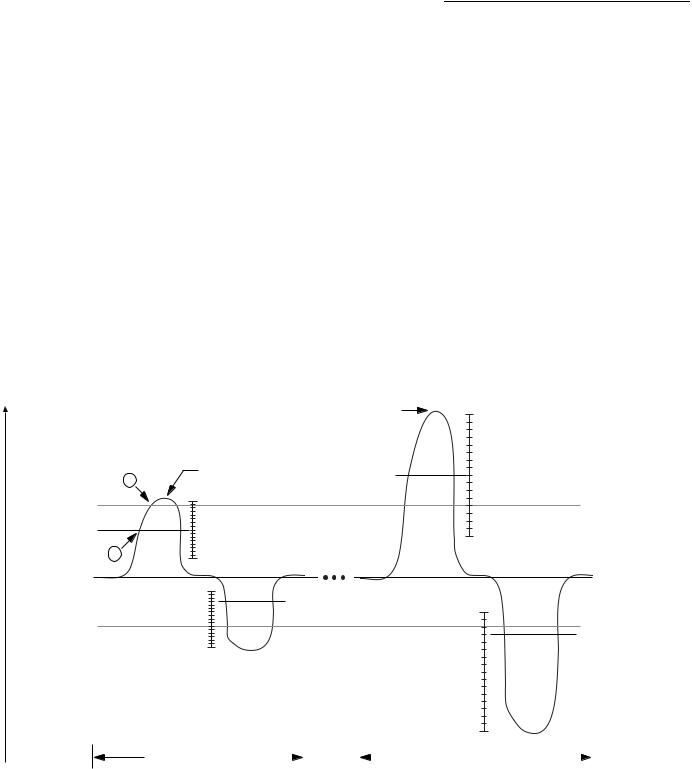
AD7142/AD7142-1 |
Preliminary Technical Data |
|
|
ADAPTIVE THRESHOLD AND SENSITIVITY
The AD7142 provides an on-chip self-learning adaptive threshold and sensitivity algorithm. This algorithm continuously monitors the output levels of each sensor and automatically rescales the threshold levels proportionally to the sensor area covered by the user. As a result, the AD7142 maintains optimal threshold and sensitivity levels for all types of users regardless of their finger sizes.
The threshold level is always referenced from the ambient level and is defined as the CDC converter output level that must be exceeded for a valid sensor contact. The sensitivity level is defined as how sensitive the sensor is before a valid contact is registered.
Figure 26 provides an example of how the adaptive threshold and sensitivity algorithm works. In a case where the adaptive threshold and sensitivity algorithm are disabled, the positive and negative sensor threshold levels are set by the
STAGE_OFFSET_HIGH and STAGE_OFFSET_LOW initial values. Reference A in Figure 26 shows that this results in an under sensitive threshold level for a small finger user, demonstrating the disadvantages of a fixed threshold level. By enabling the adaptive threshold and sensitivity algorithm, the positive and negative threshold levels are determined by the POS_THRESHOLD_SENSI TIVITY and NEG_THRESHOLD_SENSITIVITY register values and the most recent average maximum sensor output value. These registers can be used to select 16 different positive and negative sensitivity levels ranging between 25% and 95.32% of the most recent average maximum output level referenced from the ambient value. Reference B shows that the positive adaptive threshold level is set at almost mid sensitivity with a 62.51% threshold level by setting POS_THRESHOLD_SENSITIVITY = 1000. Figure 26 also provides a similar example for the negative threshold level with NEG_THRESHOLD_SENSITIVITY = 0001.
CDC OUTPUT CODES
|
|
AVERAGE MAX VALUE |
95.32% |
|
|
|
|
|
A |
AVERAGE MAX VALUE |
62.51% = POS ADAPTIVE THRESHOLD LEVEL |
|
|
||
|
|
|
|
|
|
95.32% |
STAGE_OFFSET_HIGH |
|
|
|
|
|
|
|
(INITIAL VALUE) |
|
|
62.51% = POS ADAPTIVE THRESHOLD LEVEL |
25% |
|
|
|
|
B |
|
25% |
|
|
|
|
AMBIENT LEVEL
25% NEG ADAPTIVE THRESHOLD LEVEL = 39.08%
25% |
|
|
STAGE_OFFSET_LOW |
NEG ADAPTIVE THRESHOLD LEVEL = 39.08% |
(INITIAL VALUE) |
95.32%
95.32%
SENSOR CONTACTED |
|
|
|
SENSOR CONTACTED |
-025 |
||||
|
|
|
05702 |
||||||
BY SMALL FINGER |
|
|
|
|
|
BY LARGE FINGER |
|
|
|
Figure 26. Threshold Sensitivity Example with POS_THRESHOLD_SENSITIVITY = 1000 and NEG_THRESHOLD_SENSITIVITY = 0011
Rev. PrD | Page 20 of 64
 Loading...