


Fairchild Semiconductor MM74HC4538SJ, MM74HC4538MX, MM74HC4538SJX, MM74HC4538N, MM74HC4538M Datasheet
February 1984
Revised August 2000
MM74HC4538
Dual Retriggerable Monostable Multivibrator
General Description
The MM74HC4538 high speed monostable multivibrator (one shots) is implemented in advanced silicon-gate CMOS technology. They feature speeds comparable to low power Schottky TTL circuitry while retaining the low power and high noise immunity characteristic of CMOS circuits.
Each multivibrator features both a negative, A, and a positive, B, transition triggered input, either of which can be used as an inhibit input. Also included is a clear input that when taken low resets the one shot. The MM74HC4538 is retriggerable. That is, it may be triggered repeatedly while their outputs are generating a pulse and the pulse will be extended.
Pulse width stability over a wide range of temperature and supply is achieved using linear CMOS techniques. The output pulse equation is simply: PW = 0.7(R)(C) where PW is in seconds, R is in ohms, and C is in farads. This device is pin compatible with the CD4528, and the CD4538 one shots. All inputs are protected from damage due to static discharge by diodes to VCC and ground.
Features
■Schmitt trigger on A and B inputs
■Wide power supply range: 2–6V
■Typical trigger propagation delay: 32 ns
■Fanout of 10 LS-TTL loads
■Low input current: 1 µ A max
Ordering Code:
Order Number |
Package Number |
Package Description |
|
|
|
MM74HC4538M |
M16A |
16-Lead Small Outline Integrated Circuit (SOIC), JEDEC MS-012, 0.150 Narrow |
|
|
|
MM74HC4538SJ |
M16D |
16-Lead Small Outline Package (SOP), EIAJ TYPE II, 5.3mm Wide |
|
|
|
MM74HC4538N |
N16E |
16-Lead Plastic Dual-In-Line Package (PDIP), JEDEC MS-001, 0.300 Wide |
|
|
|
Devices also available in Tape and Reel. Specify by appending the suffix letter “X” to the ordering code.
Connection Diagram |
Truth Table |
|
|
|
|
|
||
|
|
|
|
|
|
|||
|
|
|
Inputs |
|
Outputs |
|||
|
|
|
|
|
|
|
|
|
|
|
Clear |
A |
B |
Q |
|
|
|
|
|
|
Q |
|
||||
|
|
L |
X |
X |
L |
|
H |
|
|
|
X |
H |
X |
L |
|
H |
|
|
|
X |
X |
L |
L |
|
H |
|
|
|
H |
L |
↓ |
|
|
||
|
|
H |
↑ |
H |
|
|
||
|
|
|
|
|
|
|
|
|
|
H = |
HIGH Level |
|
|
|
|
|
|
|
L = LOW Level |
|
|
|
|
|
|
|
|
↑ = Transition from LOW-to-HIGH |
|
|
|
|
|
||
|
↓ = Transition from HIGH-to-LOW |
|
|
|
|
|
||
|
= One HIGH Level Pulse |
|
|
|
|
|
||
|
= One LOW Level Pulse |
|
|
|
|
|
||
|
X = Irrelevant |
|
|
|
|
|
|
|
Multivibrator Monostable Retriggerable Dual MM74HC4538
© 2000 Fairchild Semiconductor Corporation |
DS005217 |
www.fairchildsemi.com |

MM74HC4538
Block Diagrams
Note: Pin 1 and Pin 15 must be hard-wired to GND.
Logic Diagram
www.fairchildsemi.com |
2 |
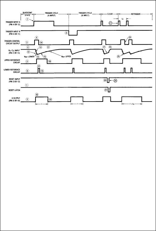
Timing Diagram
Circuit Operation
The MM74HC4538 operates as follows (refer to logic diagram). In the quiescent state, the external timing capacitor, CX, is charged to VCC. When a trigger occurs, the Q output goes HIGH and CX discharges quickly to the lower refer-
ence voltage (VREF Lower = 1/3 VCC). CX then charges, through RX, back up to the upper reference voltage (VREF
Upper = 2/3 VCC), at which point the one-shot has timed out and the Q output goes LOW.
The following, more detailed description of the circuit operation refers to both the logic diagram and the timing diagram.
QUIESCENT STATE
In the quiescent state, before an input trigger appears, the output latch is HIGH and the reset latch is HIGH (#1 in logic diagram).
Thus the Q output (pin 6 or 10) of the monostable multivibrator is LOW (#2, timing diagram).
The output of the trigger-control circuit is LOW (#3), and transistors M1, M2, and M3 are turned off. The external timing capacitor, CX, is charged to VCC (#4), and the upper reference circuit has a LOW output (#5). Transistor M4 is turned ON and transmission gate T1 is turned OFF. Thus the lower reference circuit has VCC at the noninverting input and a resulting LOW output (#6).
In addition, the output of the trigger-control reset circuit is LOW.
TRIGGER OPERATION
The MM74HC4538 is triggered by either a rising-edge signal at input A (#7) or a falling-edge signal at input B (#8), with the unused trigger input and the Reset input held at the voltage levels shown in the Truth Table. Either trigger signal will cause the output of the trigger-control circuit to go HIGH (#9).
The trigger-control circuit going HIGH simultaneously initiates three events. First, the output latch goes LOW, thus taking the Q output of the HC4538 to a HIGH State (#10). Second, transistor M3 is turned on, which allows the external timing capacitor, CX, to rapidly discharge toward ground (#11). (Note that the voltage across CXappears at the input of the upper reference circuit comparator.) Third, transistor M4 is turned off and transmission gate T1 is turned ON, thus allowing the voltage across CX to also appear at the input of the lower reference circuit comparator.
When CX discharges to the reference voltage of the lower reference circuit (#12), the outputs of both reference circuits will be HIGH (#13). The trigger-control reset circuit goes HIGH, resetting the trigger-control circuit flip-flop to a LOW State (#14). This turns transistor M3 OFF again, allowing CX to begin to charge back up toward VCC, with a time constant t = RXCX (#15). In addition, transistor M4 is turned ON and transmission gate T1 is turned OFF. Thus a high voltage level is applied to the input of the lower reference circuit comparator, causing its output to go LOW (#16). The monostable multivibrator may be retriggered at any time after the trigger-control circuit goes LOW.
When CX charges up to the reference voltage of the upper reference circuit (#17), the output of the upper reference circuit goes LOW (#18). This causes the output latch to
MM74HC4538
3 |
www.fairchildsemi.com |
 Loading...