


|
|
|
|
|
|
|
|
|
|
|
|
|
|
|
|
|
|
|
|
|
|
|
|
|
|
|
|
|
|
MPSA92 |
MMBTA92 |
PZTA92 |
|||||||||
|
|
|
|
|
|
|
|
|
|
|
|
C |
C |
|
|
|
|
|
|
|
|
|
|
|
|
|
|
|
|
|
|
|
|
|
|
|
|
|
|
E |
E |
|
|
|
|
|
|
|
|
|
|
|
|
C |
|
|
|
|
|
|
|
|
|
|
|
|
|
|
|
C |
B |
|
|
|
|
|
|
TO-92 |
SOT-23 B |
B |
|||
|
E |
SOT-223 |
|||||||||||
|
|
Mark: 2D |
|
||||||||||
|
|
|
|
|
|
|
|
|
|
|
|
|
|
PNP High Voltage Amplifier
This device is designed for high voltage driver applications.
Sourced from Process 76.
Absolute Maximum Ratings* |
TA = 25°C unless otherwise noted |
|
|
|
Symbol |
Parameter |
|
Value |
Units |
|
|
|
|
|
VCEO |
Collector-Emitter Voltage |
|
300 |
V |
|
|
|
|
|
VCBO |
Collector-Base Voltage |
|
300 |
V |
|
|
|
|
|
VEBO |
Emitter-Base Voltage |
|
5.0 |
V |
|
|
|
|
|
IC |
Collector Current - Continuous |
|
500 |
mA |
TJ, Tstg |
Operating and Storage Junction Temperature Range |
-55 to +150 |
° C |
|
|
|
|
|
|
*These ratings are limiting values above which the serviceability of any semiconductor device may be impaired.
NOTES:
1)These ratings are based on a maximum junction temperature of 150 degrees C.
2)These are steady state limits. The factory should be consulted on applications involving pulsed or low duty cycle operations.
Thermal Characteristics |
TA = 25°C unless otherwise noted |
|
|
|
||
Symbol |
Characteristic |
|
|
Max |
|
Units |
|
|
|
|
|
|
|
|
|
|
MPSA92 |
*MMBTA92 |
**PZTA92 |
|
PD |
Total Device Dissipation |
|
625 |
350 |
1,000 |
mW |
|
Derate above 25° C |
|
5.0 |
2.8 |
8.0 |
mW/° C |
Rθ JC |
Thermal Resistance, Junction to Case |
83.3 |
|
|
° C/W |
|
|
|
|
|
|
|
|
Rθ JA |
Thermal Resistance, Junction to Ambient |
200 |
357 |
125 |
° C/W |
|
|
|
|
|
|
|
|
*Device mounted on FR-4 PCB 1.6" X 1.6" X 0.06."
**Device mounted on FR-4 PCB 36 mm X 18 mm X 1.5 mm; mounting pad for the collector lead min. 6 cm2.
PZTA92 / MMBTA92 / MPSA92
2000 Fairchild Semiconductor International |
MPSA92/MMBTA92/PZTA92 Rev A |

PNP High Voltage Amplifier
(continued)
Electrical Characteristics |
TA = 25°C unless otherwise noted |
|
|
|
||
Symbol |
Parameter |
|
Test Conditions |
Min |
Max |
Units |
|
|
|
|
|
|
|
OFF CHARACTERISTICS |
|
|
|
|
|
|
V(BR)CEO |
Collector-Emitter Breakdown Voltage* |
IC = 1.0 mA, IB = 0 |
300 |
|
V |
|
V(BR)CBO |
Collector-Base Breakdown Voltage |
|
IC = 100 A, IE = 0 |
300 |
|
V |
V(BR)EBO |
Emitter-Base Breakdown Voltage |
|
IE = 100 A, IC = 0 |
5.0 |
|
V |
ICBO |
Collector-Cutoff Current |
|
VCB = 200 V, IE = 0 |
|
0.25 |
A |
IEBO |
Emitter-Cutoff Current |
|
VEB = 3.0 V, IC = 0 |
|
0.1 |
A |
ON CHARACTERISTICS* |
|
|
|
|
|
|
hFE |
DC Current Gain |
|
IC = 1.0 mA, VCE = 10 V |
25 |
|
|
|
|
|
IC = 10 mA, VCE = 10 V |
40 |
|
|
|
|
|
IC = 30 mA, VCE = 10 V |
25 |
|
|
VCE(sat) |
Collector-Emitter Saturation Voltage |
IC = 20 mA, IB = 2.0 mA |
|
0.5 |
V |
|
VBE(sat) |
Base-Emitter Saturation Voltage |
|
IC = 20 mA, IB = 2.0 mA |
|
0.9 |
V |
SMALL SIGNAL CHARACTERISTICS |
|
|
|
|
|
|
|
|
|
|
|
|
|
fT |
Current Gain - Bandwidth Product |
|
IC = 10 mA, VCE = 20 V, |
50 |
|
MHz |
|
|
|
f = 100 MHz |
|
|
|
Ccb |
Collector-Base Capacitance |
|
VCB = 20 V, IE = 0, f = 1.0 MHz |
|
6.0 |
pF |
*Pulse Test: Pulse Width ≤ 300 s, Duty Cycle ≤ 2.0%
Spice Model
PNP (Is=218.9f Xti=3 Eg=1.11 Vaf=100 Bf=99 Ne=1.307 Ise=218.9f Ikf=.2016 Xtb=1.5 Br=24.67 Nc=2 Isc=0 Ikr=0 Rc=7 Cjc=19.88p Mjc=.4876 Vjc=.75 Fc=.5 Cje=81.49p Mje=.3493 Vje=.75 Tr=516.9p Tf=1.395n Itf=1.5
Vtf=22 Xtf=270 Rb=10)
Typical Characteristics
DC Current Gain vs Collector Current
GAIN |
140 |
|
|
|
120 |
|
125 ºC |
|
|
|
|
|
||
|
|
|
|
|
CURRENT |
100 |
|
|
|
80 |
|
25 °C |
|
|
60 |
|
|
|
|
- DC |
|
- 40 ºC |
|
|
|
|
|
||
40 |
|
|
|
|
|
|
|
|
|
FE |
20 |
VCE = 5V |
|
|
h |
|
|
||
|
0 |
1 |
10 |
100 |
|
0.1 |
|||
|
|
I C - COLLECTOR CURRENT (mA) |
|
|
EMITTER-COLLECTOR (V)VOLTAGE
- CESAT V
Collector-Emitter Saturation
Voltage vs Collector Current
β |
= 10 |
|
|
0.6 |
|
|
|
0.4 |
|
|
|
|
|
|
125 ºC |
0.2 |
|
25 °C |
|
|
|
|
|
|
|
|
- 40 ºC |
0.1 |
1 |
10 |
100 |
I C - COLLECTOR CURRENT (mA)
PZTA92 / MMBTA92 / MPSA92

Typical Characteristics (continued)
|
|
Base-Emitter Saturation |
|
(V) |
|
Voltage vs Collector Current |
|
1 |
|
|
|
VOLTAGE |
|
|
|
0.9 |
|
|
|
|
|
|
|
EMITTER- |
0.8 |
- 40 ºC |
|
0.7 |
25 °C |
|
|
|
|
||
|
0.6 |
125 ºC |
|
BASE- |
|
|
|
0.4 |
|
|
|
|
0.5 |
|
|
BESAT 0.3 |
β |
= 10 |
|
|
|
||
V |
1 |
10 |
100 |
|
|||
I C - COLLECTOR CURRENT (mA)
Collector-Cutoff Current vs Ambient Temperature
(nA) |
100 |
|
|
|
|
|
|
VCB = 150V |
|
|
|
|
|
CURRENT |
|
|
|
|
|
|
10 |
|
|
|
|
|
|
|
|
|
|
|
|
|
- COLLECTOR |
1 |
|
|
|
|
|
0.1 |
|
|
|
|
|
|
|
|
|
|
|
|
|
CBO |
|
|
|
|
|
|
I |
25 |
50 |
75 |
100 |
125 |
150 |
|
TA - AMBIENT TEMPERATURE (ºC)
Gain Bandwidth Product
(MHz) |
|
|
vs Collector Current |
|
|
||
100 |
|
|
|
|
|
||
|
VCE |
= 50V |
|
|
|
||
PRODUCT |
|
|
|
|
|||
80 |
|
|
|
|
|
||
60 |
VCE |
= 15V |
|
|
|
||
BANDWIDTH |
|
|
|
||||
40 |
|
|
|
|
|
||
20 |
|
|
|
|
|
||
GAIN |
0 |
|
|
|
|
|
|
- |
1 |
10 |
20 |
50 |
100 |
||
|
|||||||
T |
|
||||||
f |
|
|
I C - COLLECTOR CURRENT (mA) |
|
|
||
|
|
|
|
|
|||
PNP High Voltage Amplifier
(continued)
|
|
|
Base-Emitter ON Voltage vs |
|
|
(V) |
0.8 |
|
Collector Current |
|
|
VOLTAGE |
|
- 40 ºC |
|
|
|
|
1 |
|
|
|
|
ON |
|
|
|
25 °C |
|
EMITTER- |
|
|
|
|
|
0.6 |
|
|
|
|
|
|
|
|
|
|
|
|
|
|
|
125 ºC |
|
BASE- |
0.4 |
|
|
VCE= 5V |
|
|
|
|
|
||
BE(ON) |
|
|
|
|
|
|
0.2 |
1 |
|
10 |
100 |
V |
|
|
|||
|
|
I C - COLLECTOR CURRENT (mA) |
|
||
|
|
|
|
||
|
|
|
Junction Capacitance |
|
|
|
|
|
vs Reverse Bias Voltage |
|
|
(pF) |
10 |
|
|
|
|
|
|
f = 1.0 MHz |
C ib |
|
|
CAPACITANCE |
|
|
|
|
|
1 |
|
|
|
|
|
|
|
|
|
|
|
JUNCTION |
|
|
|
C ob |
|
0.1 |
|
|
|
|
|
|
|
1 |
10 |
100 |
|
|
0.1 |
||||
|
|
|
V R - REVERSE VOLTAGE (V) |
|
|
Power Dissipation vs
Ambient Temperature
|
1 |
|
|
|
|
|
|
(W) |
|
|
|
|
|
|
|
DISSIPATION |
0.75 |
TO-92 |
|
SOT-223 |
|
|
|
|
|
|
|
|
|||
|
|
|
|
|
|
||
0.5 |
SOT-23 |
|
|
|
|
|
|
|
|
|
|
|
|
||
POWER |
|
|
|
|
|
|
|
0.25 |
|
|
|
|
|
|
|
- |
|
|
|
|
|
|
|
D |
|
|
|
|
|
|
|
P |
|
|
|
|
|
|
|
|
0 |
25 |
50 |
75 |
100 |
125 |
150 |
|
0 |
TEMPERATURE (oC)
PZTA92 / MMBTA92 / MPSA92

TO-92 Tape and Reel Data and Package Dimensions
TO-92 Packaging
Configuration: Figure 1.0
FSCINT Label sample |
|
|
TAPE and REEL OPTION |
|
||||
|
|
|
See Fig 2.0 for various |
|
||||
|
FAIRCHILD SEMICONDUCTOR CORPORATION |
HTB:B |
|
Reeling Styles |
|
|||
LOT: |
CBVK741B019 |
|
QTY: 10000 |
|
|
|
||
NSID: |
PN2222N |
|
SPEC: |
|
|
|
|
|
D/C1: D9842 |
|
SPEC REV: B2 |
|
|
|
|
|
|
|
|
|
QA REV: |
|
|
|
|
|
|
|
|
|
|
|
|
5 Reels per |
|
|
|
|
|
|
(FSCINT) |
|
Intermediate Box |
Customized |
F63TNR Label sample |
|
|
|
|
||||
|
|
|
|
Label |
||||
|
|
|
|
|
|
|
F63TNR |
|
LOT: CBVK741B019 |
QTY: 2000 |
|
|
|||||
FSID: PN222N |
SPEC: |
|
|
Label |
|
|||
|
|
|
|
|||||
D/C1: D9842 |
QTY1: |
SPEC REV: |
|
|
|
Customized |
|
|
|
(F63TNR)3 |
|
Label |
|
||||
D/C2: |
|
QTY2: |
N/F: F |
|
|
|||
|
CPN: |
|
|
|
|
|
||
|
|
|
|
|
|
|
|
375mm x 267mm x 375mm |
|
|
|
|
|
|
|
|
Intermediate Box |
TO-92 TNR/AMMO PACKING INFROMATION |
AMMO PACK OPTION |
|
||||||
|
|
|
|
|
|
|
||
Packing |
Style |
Quantity |
EOL code |
See Fig 3.0 for 2 Ammo |
|
|||
|
Pack Options |
|
||||||
Reel |
A |
2,000 |
|
D26Z |
|
|
||
|
|
|
|
|||||
|
|
E |
2,000 |
|
D27Z |
|
|
|
Ammo |
M |
2,000 |
|
D74Z |
|
|
|
|
|
|
P |
2,000 |
|
D75Z |
|
|
|
Unit weight |
|
|
= 0.22 gm |
|
|
FSCINT |
||
|
|
|
|
Label |
||||
Reel weight with components |
= 1.04 kg |
|
|
|||||
Ammo weight with components |
= 1.02 kg |
|
|
|
||||
Max quantity per intermediate box |
= 10,000 units |
327mm x 158mm x 135mm |
5 Ammo boxes per |
|
||||
|
|
|
|
|
|
|
||
|
|
|
|
|
|
Immediate Box |
Intermediate Box |
Customized |
|
|
|
|
|
|
|
||
|
|
|
|
|
|
|
F63TNR |
Label |
|
|
|
|
|
Customized |
|
||
|
|
|
|
|
Label |
|
||
|
|
|
|
|
Label |
333mm x 231mm x 183mm |
||
|
|
|
|
|
|
|||
|
|
|
|
|
|
|
|
|
|
|
|
|
|
|
|
|
Intermediate Box |
(TO-92) BULK PACKING INFORMATION |
|
BULK OPTION |
|
|||||
|
|
|
|
|
|
|
|
|
EOL |
|
DESCRIPTION |
LEADCLIP |
QUANTITY |
See Bulk Packing |
|
||
CODE |
|
DIMENSION |
Information table |
|
||||
|
|
|
|
|
||||
J18Z |
TO-18 OPTION STD |
NO LEAD CLIP |
2.0 K / BOX |
|
Anti-static |
|||
|
|
|
|
|
|
|
|
|
J05Z |
TO-5 |
OPTION STD |
NO LEAD CLIP |
1.5 K / BOX |
FSCINT Label |
Bubble Sheets |
||
NO EOL |
TO-92 STANDARD |
|
|
|
||||
NO LEADCLIP |
2.0 K / BOX |
|
|
|||||
CODE |
STRAIGHT |
|
|
|
||||
|
|
|
|
|
||||
|
|
|
|
|
|
|
2000 units per |
114mm x 102mm x 51mm |
|
|
|
|
|
|
|
EO70 box for |
|
|
|
|
|
|
|
|
Immediate Box |
|
|
|
|
|
|
|
|
std option |
|
|
|
|
|
|
|
|
|
|
|
|
|
|
|
|
|
|
5 EO70 boxes per |
|
|
|
|
|
|
|
|
intermediate Box |
|
|
|
|
|
|
530mm x 130mm x 83mm |
Customized |
|
|
|
|
|
|
|
Intermediate box |
||
|
|
|
|
|
|
Label |
|
|
|
|
|
|
|
|
|
|
|
FSCINT Label
10,000 units maximum per intermediate box for std option
September 1999, Rev. B
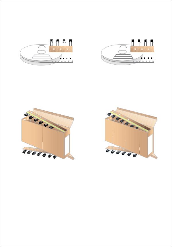
TO-92 Tape and Reel Data and Package Dimensions, continued
TO-92 Reeling Style
Configuration: Figure 2.0
Machine Option “A” (H) |
|
|
|
Machine Option “E” (J) |
|||||||||||||||||||||||
|
|
|
|
|
|
|
|
|
|
|
|
|
|
|
|
|
|
|
|
|
|
|
|
|
|
|
|
|
|
|
|
|
|
|
|
|
|
|
|
|
|
|
|
|
|
|
|
|
|
|
|
|
|
|
|
|
|
|
|
|
|
|
|
|
|
|
|
|
|
|
|
|
|
|
|
|
|
|
|
|
|
|
|
|
|
|
|
|
|
|
|
|
|
|
|
|
|
|
|
|
|
|
|
|
|
|
|
|
|
|
|
|
|
|
|
|
|
|
|
|
|
|
|
|
|
|
|
|
|
|
|
|
|
|
|
|
|
|
|
|
|
|
|
|
|
|
|
|
|
|
|
|
|
|
|
|
|
|
|
|
|
|
|
|
|
|
|
|
|
|
|
|
|
|
|
|
|
|
|
|
|
|
|
|
|
|
|
|
|
|
|
|
|
|
|
|
|
|
|
|
|
|
|
|
|
|
|
|
|
|
|
|
|
|
|
|
|
|
|
|
|
|
|
|
|
|
|
|
|
|
|
|
|
|
|
|
|
|
|
|
|
|
|
|
|
|
|
|
|
|
|
Style “A”, D26Z, D70Z (s/h) |
Style “E”, D27Z, D71Z (s/h) |
TO-92 Radial Ammo Packaging
Configuration: Figure 3.0
FIRST WIRE OFF IS COLLECTOR ADHESIVE TAPE IS ON THE TOP SIDE FLAT OF TRANSISTOR IS ON TOP
FIRST WIRE OFF IS EMITTER ADHESIVE TAPE IS ON THE TOP SIDE FLAT OF TRANSISTOR IS ON BOTTOM
ORDER STYLE |
ORDER STYLE |
D74Z (M) |
D75Z (P) |
FIRST WIRE OFF IS EMITTER (ON PKG. 92) ADHESIVE TAPE IS ON BOTTOM SIDE FLAT OF TRANSISTOR IS ON BOTTOM
FIRST WIRE OFF IS COLLECTOR (ON PKG. 92) ADHESIVE TAPE IS ON BOTTOM SIDE
FLAT OF TRANSISTOR IS ON TOP
September 1999, Rev. B
 Loading...