


MM74HC688MTC
Fairchild Semiconductor MM74HC688MTC, MM74HC688MTCX, MM74HC688WM, MM74HC688SJ, MM74HC688CW Datasheet
...
September 1983
Revised February 1999
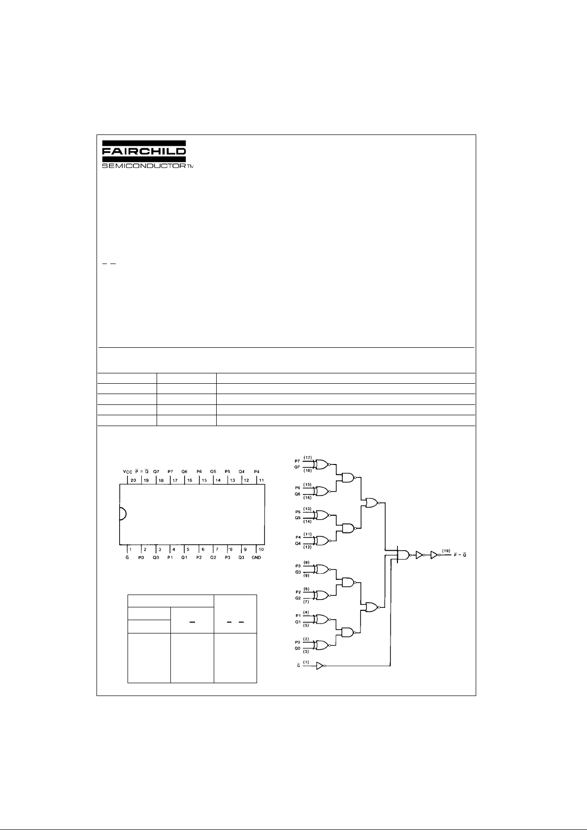
MM74HC688 8-Bit Magnitude Comparator (Equality Detector)
© 1999 Fairchild Semiconductor Corporation DS005018.prf www.fairchildsemi.com
MM74HC688
8-Bit Magnitude Comparator (Equality Detector)
General Description
The MM74HC688 equality detector utilizes advanced sili-
con-gate CMOS technolog y to com pare bit f or bit two 8-bi t
words and indicates wheth er or not they are equal. The
P
=Q output indicates equality when it is LOW. A single
active low enable is provided to facilitate cascading of se v-
eral packages and enable comparison of words greater
than 8 bits.
This device is useful in m emory block decoding applica-
tions, where memory bloc k enable signals must be ge ner-
ated from computer address information.
The comparator’s output can driv e 10 low power Schottky
equivalent loads. This comparator is functionally and pin
compatible to the 74L S688. All inputs are protected fr om
damage due to static discharge by diodes to V
CC
and
ground.
Features
■ Typical propagation delay: 20 ns
■ Wide power supply range: 2–6V
■ Low quiescent current: 80 µA (74 Series)
■ Large output current: 4 mA (74 Series)
■ Same as HC521
Ordering Code:
Devices also availab le in Tape and Reel. Specify by appending th e s uffix let t er “X” to the ordering cod e.
Connection Diagram
Pin Assignments for DIP
Top View
Truth Table
Logic Diagram
Order Number Package Number Package Description
MM74HC688WM M20B 20-Lead Small Outline Integrated Circuit (SOIC), JEDEC MS-013, 0.300” Wide
MM74HC688SJ M20D 20-Lead Small Outline Package (SOP), EIAJ TYPE II, 5.3mm Wide
MM74HC688MTC MTC20 20-Lead Thin Shrink Small Outline Package (TSSOP), JEDEC MO-153, 4.4mm Wide
MM74HC688N N20A 20-Lead Plastic Dual-In-Line Package (PDIP), JEDEC MS-001, 0.300” Wide
Inputs
Data Enable
P,Q
G
P = Q
P = QL L
P > QL H
P < QL H
XHH
www.fairchildsemi.com 2
MM74HC688
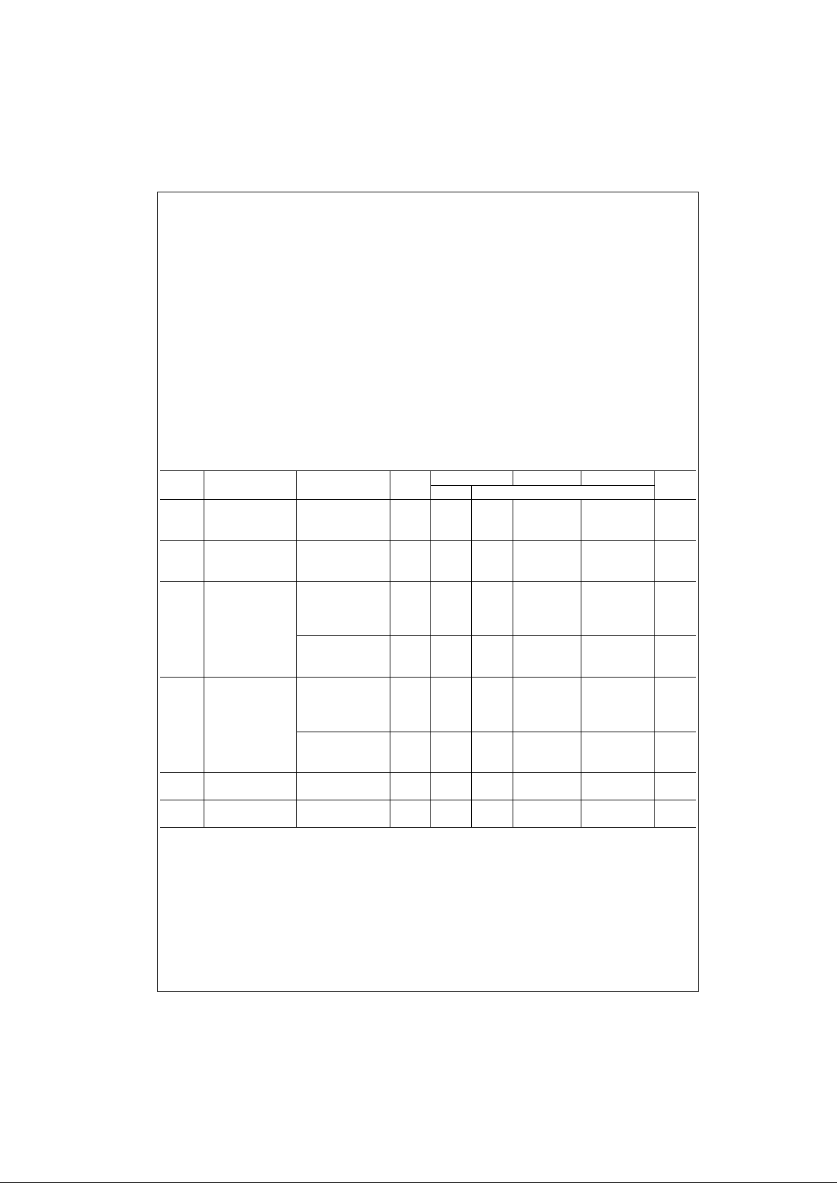
Absolute Maximum Ratings(Note 1)
(Note 2)
Recommended Operating
Conditions
Note 1: Absolute Maximum Ratings are those values beyond which dam-
age to the device may occur.
Note 2: Unless otherwise specified all voltages are referenced to ground.
Note 3: Power Dissipation temper ature dera ting — plas tic “N” packa ge: −
12 mW/°C from 65 °C to 85°C.
DC Electrical Characteristics (Note 4)
Note 4: For a power supply of 5V ±1 0% the worst c ase ou tput volta ges (V
OH
, and V
OL
) occur for HC at 4.5V. Thus the 4. 5V valu es shoul d be use d when
designing with this supply. Worst case V
IH
and V
IL
occur at V
CC
= 5.5V and 4.5V res pectively. (The V
IH
value at 5.5V is 3.85V.) The worst case leakage c ur-
rent (I
IN
, I
CC
, and I
OZ
) occur for CMOS at the higher voltage and so th e 6. 0V values should be used.
Supply Voltage (V
CC
) −0.5 to +7.0V
DC Input Voltage (V
IN
) −1.5 to V
CC
+1.5V
DC Output Voltage (V
OUT
) −0.5 to V
CC
+0.5V
Clamp Diode Current (I
IK
, I
OK
) ±20 mA
DC Output Current, per pin (I
OUT
) ±25 mA
DC V
CC
or GND Current, per pin (I
CC
) ±50 mA
Storage Temperature Range (T
STG
) −65°C to +150°C
Power Dissipation (P
D
)
(Note 3) 600 mW
S.O. Package only 500 mW
Lead Temperature (T
L
)
(Soldering 10 seconds) 260°C
Min Max Units
Supply Voltage (V
CC
)26V
DC Input or Output Voltage 0 V
CC
V
(V
IN
, V
OUT
)
Operating Temperature Range (T
A
) −40 +85 °C
Input Rise or Fall Times
(t
r
, t
f
) V
CC
= 2.0V 1000 ns
V
CC
= 4.5V 500 ns
V
CC
= 6.0V 400 ns
Symbol Parameter Conditions
V
CC
T
A
= 25°CT
A
= −40 to 85°CT
A
= −55 to 125°C
Units
Typ Guaranteed Limits
V
IH
Minimum HIGH Level 2.0V 1.5 1.5 1.5 V
Input Voltage 4.5V 3.15 3.15 3.15 V
6.0V 4.2 4.2 4.2 V
V
IL
Maximum LOW Level 2.0V 0.5 0.5 0.5 V
Input Voltage 4.5V 1.35 1.35 1.35 V
6.0V 1.8 1.8 1.8 V
V
OH
Minimum HIGH Level V
IN
= V
IH
or V
IL
Output Voltage |I
OUT
| ≤ 20 µA 2.0V 2.0 1.9 1.9 1.9 V
4.5V 4.5 4.4 4.4 4.4 V
6.0V 6.0 5.9 5.9 5.9 V
V
IN
= V
IH
or V
IL
|I
OUT
| ≤ 4.0 mA 4.5V 4.2 3.98 3.84 3.7 V
|I
OUT
| ≤ 5.2 mA 6.0V 5.7 5.48 5.34 5.2 V
V
OL
Maximum LOW Level V
IN
= V
IH
or V
IL
Output Voltage |I
OUT
| ≤ 20 µA 2.0V 0 0.1 0.1 0.1 V
4.5V 0 0.1 0.1 0.1 V
6.0V 0 0.1 0.1 0.1 V
V
IN
= V
IH
or V
IL
|I
OUT
| ≤ 4.0 mA 4.5V 0.2 0.26 0.33 0.4 V
|I
OUT
| ≤ 5.2 mA 6.0V 0.2 0.26 0.33 0.4 V
I
IN
Maximum Input V
IN
= V
CC
or GND 6.0V ±0.1 ±1.0 ±1.0 µA
Current
I
CC
Maximum Quiescent V
IN
= V
CC
or GND 6.0V 8.0 80 160 µA
Supply Current I
OUT
= 0 µA
 Loading...