


MM74HC139MTC
Fairchild Semiconductor MM74HC139MTC, MM74HC139MX, MM74HC139N, MM74HC139SJ, MM74HC139M Datasheet
...
September 1983
Revised February 1999
MM74HC139 Dual 2-To-4 Line Decoder
© 1999 Fairchild Semiconductor Corporation DS005311.prf www.fairchildsemi.com
MM74HC139
Dual 2-To-4 Line Decoder
General Description
The MM74HC139 decoder utilizes advanced silicon-gate
CMOS technology, and is well suite d to memory address
decoding or data routing applications. It possesses the
high noise immunity and l ow power consumption usually
associated with CMOS circuitry, yet has speeds compar a-
ble to low power Schottky TTL logic.
The MM74HC139 contain two independent one-of-four
decoders each with a single active low enable input (G1, or
G2). Data on the select inputs (A 1, and B1 or A2, an d B2)
cause one of the four normally high outputs to go LOW.
The decoder’s outputs can drive 10 low power Schottky
TTL equivalent lo ads, and are functionally a s well as pin
equivalent to the 74LS 139. All inputs are protected from
damage due to static discharge by diodes to V
CC
and
ground.
Features
■ Typical propagation delays —
Select to outputs (4 delays): 18 ns
Select to output (5 delays): 28 ns
Enable to output: 20 ns
■ Low power: 40 µW quiescent s upply power
■ Fanout of 10 LS-TTL devices
■ Input current maximum 1 µA, typical 10 pA
Ordering Code:
Devices also availab le in Tape and Reel. Specify by appending th e s uffix let t er “X” to the ordering cod e.
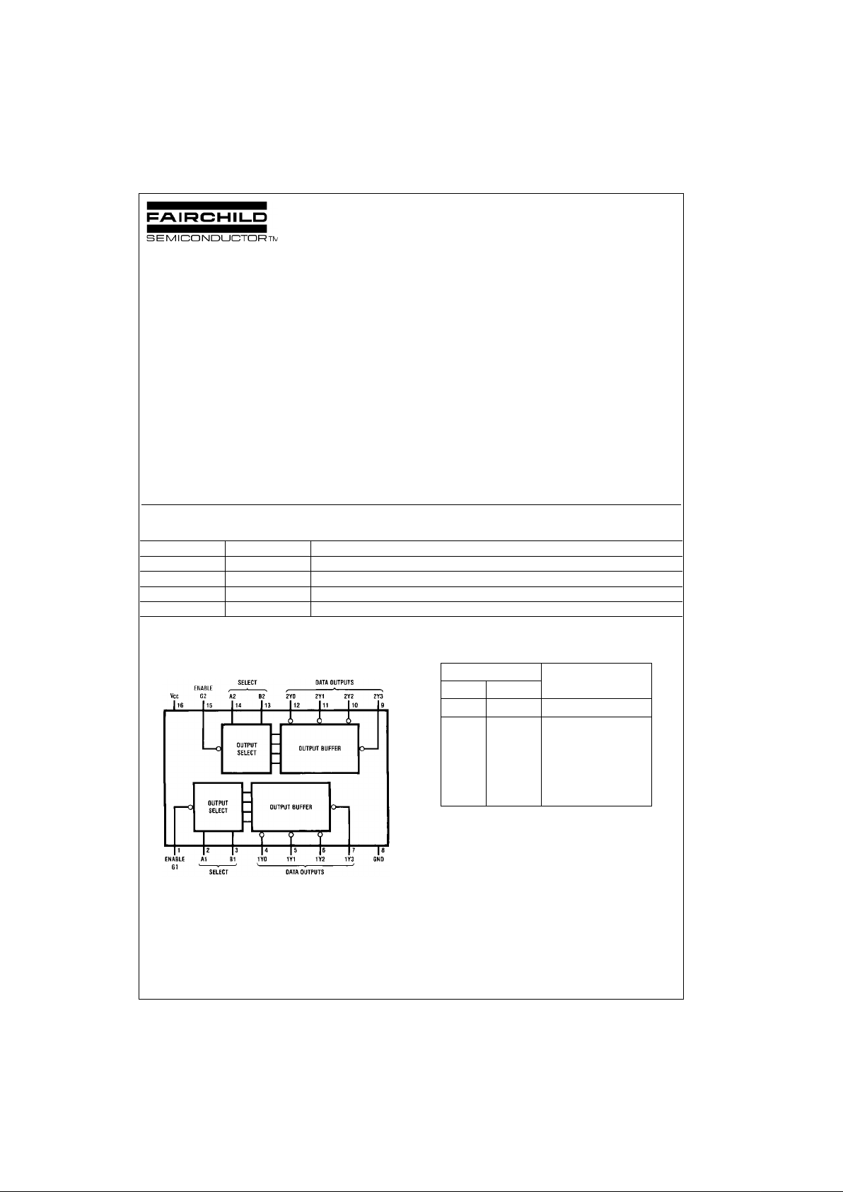
Connection Diagram
Pin Assignments f or DIP, SOIC, SOP and TSSOP
Truth Table
H = HIGH Level
L = LOW Level
X = Don't Care
Order Number Package Number Package Description
MM74HC139M M16A 16-Lead Small Outline Integrated Circuit (SOIC), JEDEC MS-012, 0.150” Narrow
MM74HC139SJ M16D 16-Lead Small Outline Package (SOP), EIAJ TYPE II, 5.3mm Wide
MM74HC139MTC MTC16 16-Lead Thin Shrink Small Outline Package (TSSOP) JEDEC MO-153, 4.4mm Wide
MM74HC139N N16E 16-Lead Plastic Dual-In-Line Package (PDIP), JEDEC MS-001, 0.300” Wide
Inputs Outputs
Enable Select
G B A Y0Y1Y2Y3
H XXHHHH
LLLLHHH
LLHHLHH
LHLHHLH
L HHHHHL

www.fairchildsemi.com 2
MM74HC139
Logic Diagram
(1 of 2)
3 www.fairchildsemi.com
MM74HC139
Absolute Maximum Ratings(Note 1)
(Note 2)
Recommended Operating
Conditions
Note 1: Absolute Maximum Ra tings are those valu es beyond w hich dam-
age to the device may occur.
Note 2: Unless otherwise specified all voltages are referenced to ground.
Note 3: Power Dissipation te mperature d erating — pl astic “N” pa ckage: −
12 mW/°C from 65°C to 85°C.
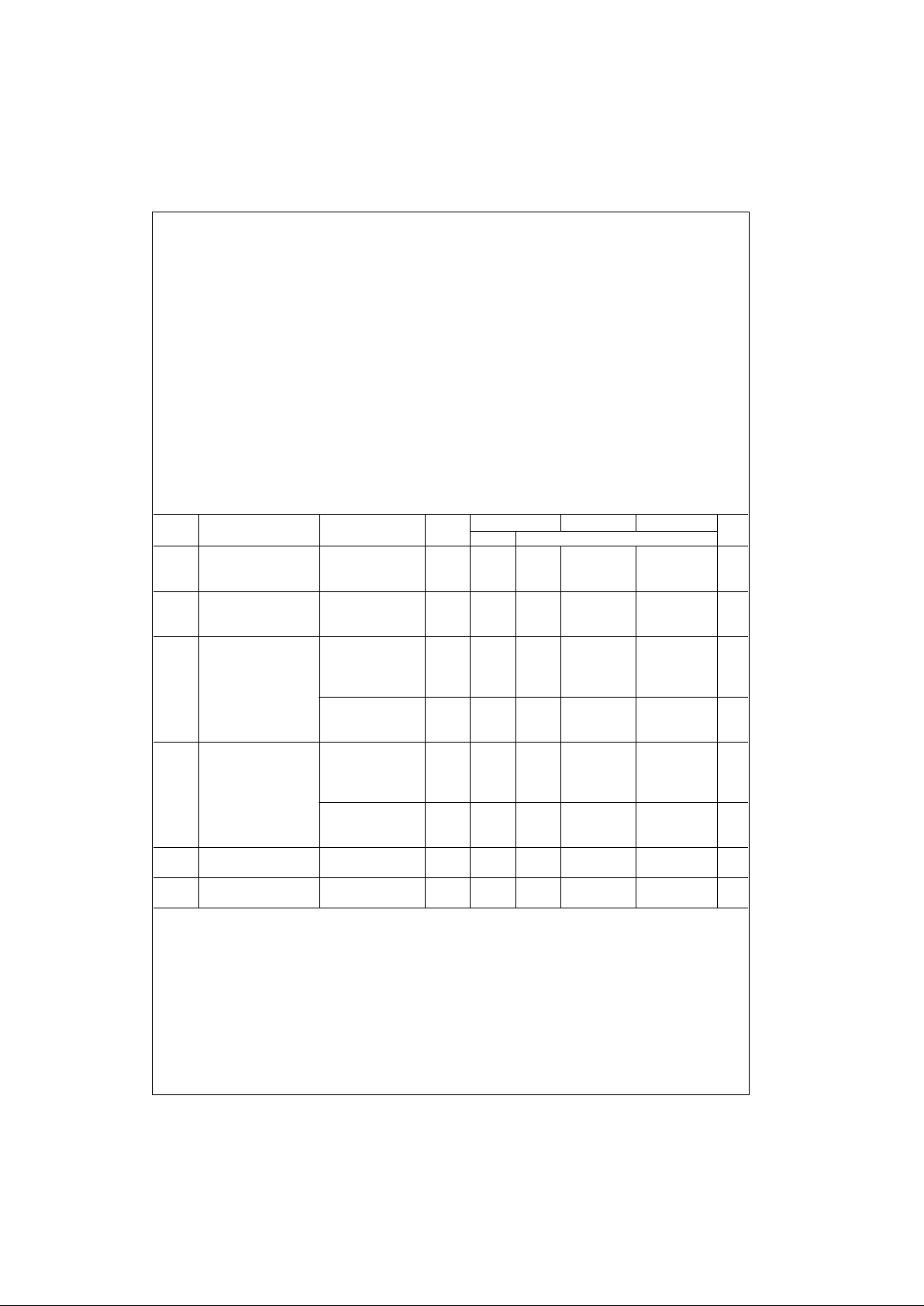
DC Electrical Characteristics (Note 4)
Note 4: For a powe r supply o f 5V ±10% the worst case output voltages (V
OH
, and V
OL
) occur for HC at 4.5V. Thus the 4. 5V valu es shou ld be u sed when
designing with this supply. Worst case V
IH
and V
IL
occur at V
CC
= 5.5V and 4.5V respectively. (The V
IH
value at 5.5V is 3 .8 5V.) The worst c as e leakage cur-
rent (I
IN
, I
CC
, and I
OZ
) occur for CMOS at the higher voltage and so th e 6. 0V values should be used.
Supply Voltage (V
CC
) −0.5 to +7.0V
DC Input Voltage (V
IN
) −1.5 to V
CC
+1.5V
DC Output Voltage (V
OUT
) −0.5 to V
CC
+0.5V
Clamp Diode Current (I
IK
, I
OK
) ±20 mA
DC Output Current, per pin (I
OUT
) ±25 mA
DC V
CC
or GND Current, per pin (I
CC
) ±50 mA
Storage Temperature Range (T
STG
) −65°C to +150°C
Power Dissipation (P
D
)
(Note 3) 600 mW
S.O. Package only 500 mW
Lead Temperature (T
L
)
(Solderi ng 10 seconds) 260°C
Min Max Units
Supply Voltage (V
CC
)26V
DC Input or Output Voltage 0 V
CC
V
(V
IN
, V
OUT
)
Operating Temperature Range (T
A
) −40 +85 °C
Input Rise or Fall Times
(t
r
, t
f
) V
CC
= 2.0V 1000 ns
V
CC
= 4.5V 500 ns
V
CC
= 6.0V 400 ns
Symbol Parameter Conditions
V
CC
T
A
= 25°CT
A
= −40 to 85°CT
A
= −55 to 125°C
Units
Typ Guaranteed Limits
V
IH
Minimum HIGH Level 2.0V 1.5 1.5 1.5 V
Input Voltage 4.5V 3.15 3.15 3.15 V
6.0V 4.2 4.2 4.2 V
V
IL
Maximum LOW Level 2.0V 0.5 0.5 0.5 V
Input Voltage 4.5V 1.35 1.35 1.35 V
6.0V 1.8 1.8 1.8 V
V
OH
Minimum HIGH Level V
IN
= V
IH
or V
IL
Output Voltage |I
OUT
| ≤ 20 µA 2.0V 2.0 1.9 1.9 1.9 V
4.5V 4.5 4.4 4.4 4.4 V
6.0V 6.0 5.9 5.9 5.9 V
V
IN
= V
IH
or V
IL
|I
OUT
| ≤ 4.0 mA 4.5V 4.2 3.98 3.84 3.7 V
|I
OUT
| ≤ 5.2 mA 6.0V 5.7 5.48 5.34 5.2 V
V
OL
Maximum LOW Level V
IN
= V
IH
or V
IL
Output Voltage |I
OUT
| ≤ 20 µA 2.0V 0 0.1 0.1 0.1 V
4.5V 0 0.1 0.1 0.1 V
6.0V 0 0.1 0.1 0.1 V
V
IN
= V
IH
or V
IL
|I
OUT
| ≤ 4.0 mA 4.5V 0.2 0.26 0.33 0.4 V
|I
OUT
| ≤ 5.2 mA 6.0V 0.2 0.26 0.33 0.4 V
I
IN
Maximum Input V
IN
= V
CC
or GND 6.0V ±0.1 ±1.0 ±1.0 µA
Current
I
CC
Maximum Quiescent V
IN
= V
CC
or GND 6.0V 8.0 80 160 µA
Supply Current I
OUT
= 0 µA
 Loading...