


October 1987
Revised January 1999
MM74C925 • MM74C926 • MM74C927 • MM74C928 4-Digit Counters with Multiplexed
7-Segment Output Drivers
General Description
The MM74C925, MM74C926, MM74C927 and MM74C928 CMOS counters consist of a 4-digit counter, an internal output latch, NPN output sourcing drivers for a 7-segment display, and an internal multiplexing circuitry with four multiplexing outputs. The multiplexing circuit has its own free-running oscillator, and requires no external clock. The counters advance on negative edge of clock. A HIGH signal on the Reset input will reset the counter to zero, and reset the carry-out LOW. A LOW signal on the Latch Enable input will latch the number in the counters into the internal output latches. A HIGH signal on Display Select input will select the number in the counter to be displayed; a LOW level signal on the Display Select will select the number in the output latch to be displayed.
The MM74C925 is a 4-decade counter and has Latch Enable, Clock and Reset inputs.
The MM74C926 is like the MM74C925 except that it has a display select and a carry-out used for cascading counters. The carry-out signal goes HIGH at 6000, goes back LOW at 0000.
The MM74C927 is like the MM74C926 except the second most significant digit divides by 6 rather than 10. Thus, if the clock input frequency is 10 Hz, the display would read tenths of seconds and minutes (i.e., 9:59.9).
The MM74C928 is like the MM74C926 except the most significant digit divides by 2 rather than 10 and the carry-out is an overflow indicator which is HIGH at 2000, and it goes
back LOW only when the counter is reset. Thus, this is a 3½-digit counter.
Features
■Wide supply voltage range: 3V to 6V
■Guaranteed noise margin: 1V
■High noise immunity: 0.45 VCC (typ.)
■High segment sourcing current: 40 mA @ VCC − 1.6V, VCC = 5V
■Internal multiplexing circuitry
Design Considerations
Segment resistors are desirable to minimize power dissipation and chip heating. The DS75492 serves as a good digit driver when it is desired to drive bright displays. When using this driver with a 5V supply at room temperature, the display can be driven without segment resistors to full illumination. The user must use caution in this mode however, to prevent overheating of the device by using too high a supply voltage or by operating at high ambient temperatures.
The input protection circuitry consists of a series resistor, and a diode to ground. Thus input signals exceeding VCC will not be clamped. This input signal should not be allowed to exceed 15V.
Ordering Code:
Order Number |
Package Number |
Package Description |
|
|
|
MM74C925N |
N16E |
16-Lead Plastic Dual-In-Line Package (PDIP), JEDEC MS-001, 0.300” Wide |
|
|
|
MM74C926N |
N18A |
18-Lead Plastic Dual-In-Line Package (PDIP), JEDEC MS-001, 0.300” Wide |
|
|
|
MM74C927N |
N18A |
18-Lead Plastic Dual-In-Line Package (PDIP), JEDEC MS-001, 0.300” Wide |
|
|
|
MM74C928N |
N18A |
18-Lead Plastic Dual-In-Line Package (PDIP), JEDEC MS-001, 0.300” Wide |
|
|
|
Drivers Output Segment-7 Multiplexed with Counters Digit-4 MM74C928 • MM74C927 • MM74C926 • MM74C925
© 1999 Fairchild Semiconductor Corporation |
DS005919.prf |
www.fairchildsemi.com |
MM74C925 • MM74C926 • MM74C927 • MM74C928
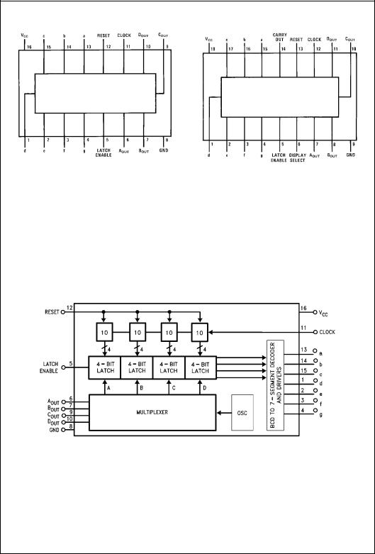
Connection Diagrams
Pin Assignments for DIP
Top View |
Top View |
|
MM74C925 |
||
MM74C926, MM74C927, MM74C928 |
||
|
Functional Description
Reset — Asynchronous, active high
Display Select — High, displays output of counter
Low, displays output of latch Latch Enable — High, flow through condition
|
Low, latch condition |
Clock |
—Negative edge sensitive |
Segment Output — Current sourcing with 40 mA @V OUT = VCC − 1.6V (typ.) Also, sink capability = 2 LTTL loads
Digit Output — Current sourcing with 1 mA @V OUT = 1.75V. Also, sink capability = 2 LTTL loads
Carry-Out — 2 LTTL loads. See carry-out waveforms.
Logic Diagrams
MM74C925
www.fairchildsemi.com |
2 |

Logic Diagrams (Continued)
MM74C926
MM74C927
MM74C928
MM74C928 • MM74C927 • MM74C926 • MM74C925
3 |
www.fairchildsemi.com |
 Loading...