


Fairchild Semiconductor MM74HC32MX, MM74HC32MTC, MM74HC32CW, MM74HC32SJX, MM74HC32N Datasheet
...
September 1983
Revised February 1999
MM74HC32
Quad 2-Input OR Gate
General Description
The MM74HC32 OR gates utilize advanced silicon-gate CMOS technology to achieve operating speeds similar to LS-TTL gates with the low power consumption of standard CMOS integrated circuits. All gates have buffered outputs providing high noise immunity and the ability to drive 10 LS-TTL loads. The 74HC logic family is functionally as well as pin-out compatible with the standard 74LS logic family.
All inputs are protected from damage due to static discharge by internal diode clamps to VCC and ground.
Features
■Typical propagation delay: 10 ns
■Wide power supply range: 2–6V
■Low quiescent current: 20 μA maximum (74HC Series)
■Low input current: 1 μA maximum
■Fanout of 10 LS-TTL loads
Ordering Code:
Order Number |
Package Number |
Package Description |
|
|
|
MM74HC32M |
M14A |
14-Lead Small Outline Integrated Circuit (SOIC), JEDEC MS-120, 0.150” Narrow |
|
|
|
MM74HC32SJ |
M14D |
14-Lead Small Outline Package (SOP), EIAJ TYPE II, 5.3mm Wide |
|
|
|
MM74HC32MTC |
MTC14 |
14-Lead Thin Shrink Small Outline Package (TSSOP), JEDEC MO-153, 4.4mm Wide |
|
|
|
MM74HC32N |
N14A |
14-Lead Plastic Dual-In-Line Package (PDIP), JEDEC MS-001, 0.300” Wide |
|
|
|
Devices also available in Tape and Reel. Specify by appending suffix letter “X” to the ordering code.
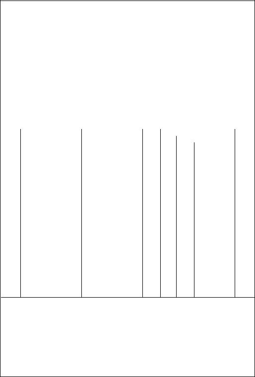
Connection Diagram
Pin Assignments for DIP, SOIC, SOP and TSSOP
Top View
Logic Diagram
Y = A + B
(1 of 4)
Gate OR Input-2 Quad MM74HC32
© 1999 Fairchild Semiconductor Corporation |
DS005132.prf |
www.fairchildsemi.com |
MM74HC32
Absolute Maximum Ratings(Note 1)
(Note 2) |
|
Supply Voltage (VCC) |
−0.5 to + 7.0V |
DC Input Voltage (VIN) |
−1.5 to VCC + 1.5V |
DC Output Voltage (VOUT) |
−0.5 to VCC + 0.5V |
Clamp Diode Current (IIK, IOK) |
±20 mA |
DC Output Current, per pin (IOUT) |
±25 mA |
DC VCC or GND Current, per pin (ICC) |
±50 mA |
Storage Temperature Range (TSTG) |
−65°C to +150°C |
Power Dissipation (PD) |
|
(Note 3) |
600 mW |
S.O. Package only |
500 mW |
Lead Temperature (TL) |
260°C |
(Soldering 10 seconds) |
Recommended Operating
Conditions
|
Min |
Max |
Units |
Supply Voltage (VCC) |
2 |
6 |
V |
DC Input or Output Voltage |
0 |
VCC |
V |
(VIN, VOUT) |
−40 |
+85 |
°C |
Operating Temperature Range (TA) |
|||
Input Rise or Fall Times |
|
|
|
(tr, tf) VCC = 2.0V |
|
1000 |
ns |
VCC = 4.5V |
|
500 |
ns |
VCC = 6.0V |
|
400 |
ns |
Note 1: Absolute Maximum Ratings are those values beyond which damage to the device may occur.
Note 2: Unless otherwise specified all voltages are referenced to ground.
Note 3: Power Dissipation temperature derating — plastic “N” package: − 12 mW/°C from 65°C to 85°C.
DC Electrical Characteristics (Note 4)
Symbol |
Parameter |
Conditions |
VCC |
TA = 25°C |
TA = −40 to 85°C |
Units |
||
Typ |
Guaranteed Limits |
|||||||
|
|
|
|
|
||||
|
|
|
|
|
|
|
|
|
VIH |
Minimum HIGH Level |
|
2.0V |
|
1.5 |
1.5 |
V |
|
|
Input Voltage |
|
4.5V |
|
3.15 |
3.15 |
V |
|
|
|
|
6.0V |
|
4.2 |
4.2 |
V |
|
|
|
|
|
|
|
|
|
|
VIL |
Maximum LOW Level |
|
2.0V |
|
0.5 |
0.5 |
V |
|
|
Input Voltage |
|
4.5V |
|
1.35 |
1.35 |
V |
|
|
|
|
6.0V |
|
1.8 |
1.8 |
V |
|
|
|
|
|
|
|
|
|
|
VOH |
Minimum HIGH Level |
VIN = VIH or VIL |
|
|
|
|
|
|
|
Output Voltage |
|IOUT | ≤ 20 μA |
2.0V |
2.0 |
1.9 |
1.9 |
V |
|
|
|
|
4.5V |
4.5 |
4.4 |
4.4 |
V |
|
|
|
|
6.0V |
6.0 |
5.9 |
5.9 |
V |
|
|
|
|
|
|
|
|
|
|
|
|
VIN = VIH or VIL |
|
|
|
|
|
|
|
|
| IOUT | ≤ 4.0 mA |
4.5V |
4.7 |
3.98 |
3.84 |
V |
|
|
|
| IOUT | ≤ 5.2 mA |
6.0V |
5.2 |
5.48 |
5.34 |
V |
|
VOL |
Maximum LOW Level |
VIN = VIL |
|
|
|
|
|
|
|
Output Voltage |
|IOUT | ≤ 20 μA |
2.0V |
0 |
0.1 |
0.1 |
V |
|
|
|
|
4.5V |
0 |
0.1 |
0.1 |
V |
|
|
|
|
6.0V |
0 |
0.1 |
0.1 |
V |
|
|
|
|
|
|
|
|
|
|
|
|
VIN = VIL |
|
|
|
|
|
|
|
|
| IOUT | ≤ 4.0 mA |
4.5V |
0.2 |
0.26 |
0.33 |
V |
|
|
|
| IOUT | ≤ 5.2 mA |
6.0V |
0.2 |
0.26 |
0.33 |
V |
|
IIN |
Maximum Input |
VIN = VCC or GND |
6.0V |
|
±0.1 |
±1.0 |
μA |
|
|
Current |
|
|
|
|
|
|
|
|
|
|
|
|
|
|
|
|
ICC |
Maximum Quiescent |
VIN = VCC or GND |
6.0V |
|
2.0 |
20 |
μA |
|
|
Supply Current |
IOUT = 0 μA |
|
|
|
|
|
|
Note 4: For a power supply of 5V ±10% the worst case output voltages (VOH, and VOL) occur for HC at 4.5V. Thus the 4.5V values should be used when designing with this supply. Worst case VIH and VIL occur at VCC = 5.5V and 4.5V respectively. (The VIH value at 5.5V is 3.85V.) The worst case leakage current (IIN, ICC, and IOZ) occur for CMOS at the higher voltage and so the 6.0V values should be used.
www.fairchildsemi.com |
2 |
 Loading...