


MM74HC154WMX
Fairchild Semiconductor MM74HC154WMX, MM74HC154N, MM74HC154MTC, MM74HC154WM, MM74HC154MTCX Datasheet
September 1983
Revised February 1999
MM74HC154 4-to-16 Line Decoder
© 1999 Fairchild Semiconductor Corporation DS005122.prf www.fairchildsemi.com
MM74HC154
4-to-16 Line Decoder
General Description
The MM74HC154 decoder utilizes advanced silicon-gate
CMOS technology, and is well suite d to memory address
decoding or data routing applications. It posse sses high
noise immunity, and low power consumption of CMOS with
speeds similar to low power Schottky TTL circuits.
The MM74HC154 have 4 binary select inputs (A, B, C, and
D). If the device is e nabled these inputs de termine which
one of the 16 normally HIGH outputs will go LOW. Two
active LOW enables (G1
and G2) are provided to ease
cascading of decoders with little or no external logic.
Each output can drive 10 low p ower Schottk y TTL eq uiva-
lent loads, and is functionally and pin equivalent to the
74LS154. All inputs are protected from damage due to
static discharge by diodes to V
CC
and ground.
Features
■ Typical propagation delay: 21 ns
■ Power supp ly quiescent current: 80 µA
■ Wide power supply voltage range: 2–6V
■ Low input current: 1 µA maximum
Ordering Code:
Devices also availab le in Tape and Reel. Specify by appending th e s uffix let t er “X” to the ordering cod e.
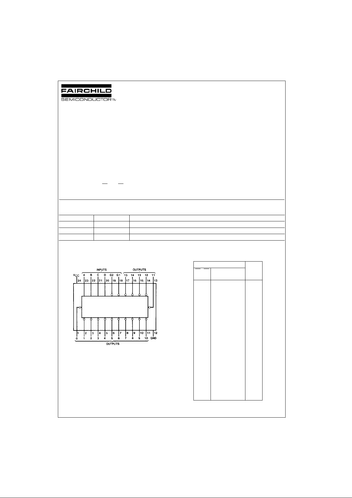
Connection Diagram
Pin Assignments for DIP, SOIC and TSSOP
Top View
Truth Table
Note 1: All others HIGH
Order Number Package Number Package Description
MM74HC154WM M24B 24-Lead Small Outline Integrated Circuit (SOIC), JEDEC MS-013, 0.300” Wide Body
MM74HC154MTC MTC24 24-Lead Thin Shrink Small Outline Package (TSSOP), JEDEC MO-153, 4.4mm Wide
MM74HC154N N24C 24-Lead Plastic Dual-In-Line Package (PDIP), JEDEC MS-100, 0.300” Wide
Inputs Low
G1
G2 DCBAOutput
(Note 1)
LLLLLL 0
LLLLLH 1
LLLLHL 2
LLLLHH 3
LLLHLL 4
LLLHLH 5
LLLHHL 6
LLLHHH 7
LLHLLL 8
LLHLLH 9
LLHLHL 10
LLHLHH 11
LLHHLL 12
LLHHLH 13
LLHHHL 14
LLHHHH 15
LHXXXX —
HLXXXX —
HHXXXX —
www.fairchildsemi.com 2
MM74HC154
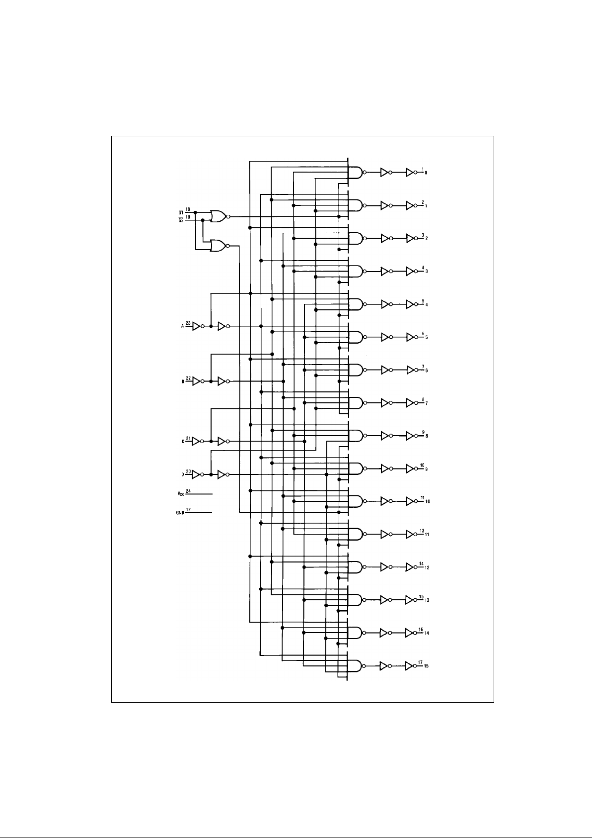
Logic Diagram
3 www.fairchildsemi.com
MM74HC154
Absolute Maximum Ratings(Note 2)
(Note 3)
Recommended Operating
Conditions
Note 2: Absolute Maximum Ra tings are those valu es beyond w hich dam-
age to the device may occur.
Note 3: Unless otherwise specified all voltages are referenced to ground.
Note 4: Power Dissipation te mperature d erating — pl astic “N” pa ckage: −
12 mW/°C from 65°C to 85°C.
DC Electrical Characteristics (Note 5)
Note 5: For a powe r supply o f 5V ±10% the worst case output voltages (V
OH
, and V
OL
) occur for HC at 4.5V. Thus the 4. 5V valu es shou ld be u sed when
designing with this supply. Worst case V
IH
and V
IL
occur at V
CC
= 5.5V and 4.5V respectively. (The V
IH
value at 5.5V is 3 .8 5V.) The worst c as e leakage cur-
rent (I
IN
, I
CC
, and I
OZ
) occur for CMOS at the higher voltage and so th e 6. 0V values should be used.
Supply Voltage (V
CC
) −0.5 to +7.0V
DC Input Voltage (V
IN
) −1.5 to V
CC
+1.5V
DC Output Voltage (V
OUT
) −0.5 to V
CC
+0.5V
Clamp Diode Current (I
IK
, I
OK
) ±20 mA
DC Output Current, per pin (I
OUT
) ±25 mA
DC V
CC
or GND Current, per pin (I
CC
) ±50 mA
Storage Temperature Range (T
STG
) −65°C to +150°C
Power Dissipation (P
D
)
(Note 4) 600 mW
S.O. Package only 500 mW
Lead Temperature (T
L
)
(Solderi ng 10 seconds) 260°C
Min Max Units
Supply Voltage (V
CC
)26V
DC Input or Output Voltage (V
IN
, V
OUT
)0V
CC
V
Operating Temperature Range (T
A
) −40 +85 °C
Input Rise or Fall Times
(t
r
, t
f
) V
CC
= 2.0V 1000 ns
V
CC
= 4.5V 500 ns
V
CC
= 6.0V 400 ns
Symbol Parameter Conditions
V
CC
T
A
= 25°CT
A
= −40 to 85°C
Units
Typ Guaranteed Limits
V
IH
Minimum HIGH 2.0V 1.5 1.5 V
Level Input 4.5V 3.15 3.15 V
Voltage 6.0V 4.2 4.2 V
V
IL
Maximum LOW 2.0V 0.5 0.5 V
Level Input 4.5V 1.35 1.35 V
Voltage 6.0V 1.8 1.8 V
V
OH
Minimum HIGH V
IN
= V
IH
or V
IL
Level Output |I
OUT
| ≤ 20 µA 2.0V 2.0 1.9 1.9 V
Voltage 4.5V 4.5 4.4 4.4 V
6.0V 6.0 5.9 5.9 V
V
IN
= V
IH
or V
IL
|I
OUT
| ≤ 4.0 mA 4.5V 4.2 3.98 3.84 V
|I
OUT
| ≤ 5.2 mA 6.0V 5.7 5.48 5.34 V
V
OL
Maximum LOW V
IN
= V
IH
or V
IL
Level Output |I
OUT
| ≤ 20 µA 2.0V 0 0.1 0.1 V
Voltage 4.5V 0 0.1 0.1 V
6.0V 0 0.1 0.1 V
V
IN
= V
IH
or V
IL
|I
OUT
| ≤ 4.0 mA 4.5V 0.2 0.26 0.33 V
|I
OUT
| ≤ 5.2 mA 6.0V 0.2 0.26 0.33 V
I
IN
Maximum V
IN
= V
CC
or GND 6.0V ±0.1 ±1.0 µA
Input Current
I
CC
Maximum V
IN
= V
CC
or GND 6.0V 8.0 80 µA
Quiescent I
OUT
= 0 µA
Supply Current
 Loading...