


Fairchild Semiconductor MM74HCT244SJ, MM74HCT244SJX, MM74HCT244WM, MM74HCT244WMX, MM74HCT244MTC Datasheet
...
February 1984
Revised July 1999
MM74HCT240 • MM74HCT244
Inverting Octal 3-STATE Buffer • Octal 3-STATE Buffer
General Description
The MM74HCT240 and MM74HCT244 3-STATE buffers utilize advanced silicon-gate CMOS technology and are general purpose high speed inverting and non-inverting buffers. They possess high drive current outputs which enable high speed operation even when driving large bus capacitances. These circuits achieve speeds comparable to low power Schottky devices, while retaining the low power consumption of CMOS. All three devices are TTL input compatible and have a fanout of 15 LS-TTL equivalent inputs.
MM74HCT devices are intended to interface between TTL and NMOS components and standard CMOS devices. These parts are also plug-in replacements for LS-TTL devices and can be used to reduce power consumption in existing designs.
The MM74HCT240 is an inverting buffer and the MM74HCT244 is a non-inverting buffer. Each device has two active low enables (1G and 2G), and each enable independently controls 4 buffers.
All inputs are protected from damage due to static discharge by diodes to VCC and Ground.
Features
■TTL input compatible
■Typical propagation delay: 14 ns
■3-STATE outputs for connection to system buses
■Low quiescent current: 80 μA
■High output drive current: 6 mA (min)
Ordering Code:
Order Number |
Package Number |
Package Description |
|
|
|
MM74HCT240WM |
M20B |
20-Lead Small Outline Integrated Circuit (SOIC), JEDEC MS-013, 0.300” Wide |
|
|
|
MM74HCT240SJ |
M20D |
20-Lead Small Outline Package (SOP), EIAJ TYPE II, 5.3mm Wide |
|
|
|
MM74HCT240MTC |
MTC20 |
20-Lead Thin Shrink Small Outline Package (TSSOP), JEDEC MO-153, 4.4mm Wide |
|
|
|
MM74HCT240N |
N20A |
20-Lead Plastic Dual-In-Line Package (PDIP), JEDEC MS-001, 0.300” Wide |
|
|
|
MM74HCT244WM |
M20B |
20-Lead Small Outline Integrated Circuit (SOIC), JEDEC MS-013, 0.300” Wide |
|
|
|
MM74HCT244SJ |
M20D |
20-Lead Small Outline Package (SOP), EIAJ TYPE II, 5.3mm Wide |
|
|
|
MM74HCT244MTC |
MTC20 |
20-Lead Thin Shrink Small Outline Package (TSSOP), JEDEC MO-153, 4.4mm Wide |
|
|
|
MM74HCT244N |
N20A |
20-Lead Plastic Dual-In-Line Package (PDIP), JEDEC MS-001, 0.300” Wide |
|
|
|
Devices also available in Tape and Reel. Specify by appending the suffix letter “X” to the ordering code.
Connection Diagrams
Pin Assignments for DIP, SOIC, SOP and TSSOP
Top View |
Top View |
MM74HCT240 |
MM74HCT244 |
Buffer STATE-3 Octal • Buffer STATE-3 Octal Inverting MM74HCT244 • MM74HCT240
© 1999 Fairchild Semiconductor Corporation |
DS005365 |
www.fairchildsemi.com |
MM74HCT240 • MM74HCT244
Truth Tables
MM74HCT240
1G |
1A |
1Y |
2G |
2A |
2Y |
|
|
|
|
|
|
L |
L |
H |
L |
L |
H |
L |
H |
L |
L |
H |
L |
H |
L |
Z |
H |
L |
Z |
H |
H |
Z |
H |
H |
Z |
|
|
|
|
|
|
H = HIGH Level
L = LOW Level
Z = High Impedance
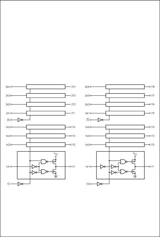
Logic Diagrams
MM74HCT240
MM74HCT244
1G |
1A |
1Y |
2G |
2A |
2Y |
|
|
|
|
|
|
L |
L |
L |
L |
L |
L |
L |
H |
H |
L |
H |
H |
H |
L |
Z |
H |
L |
Z |
H |
H |
Z |
H |
H |
Z |
|
|
|
|
|
|
MM74HCT244
www.fairchildsemi.com |
2 |

Absolute Maximum Ratings(Note 1)
(Note 2) |
|
Supply Voltage (VCC) |
−0.5 to +7.0V |
DC Input Voltage (VIN) |
−1.5 to VCC +1.5V |
DC Output Voltage (VOUT) |
−0.5 to VCC +0.5V |
Clamp Diode Current (IIK, IOK) |
±20 mA |
DC Output Current, per pin (IOUT) |
±35 mA |
DC VCC or GND Current, per pin (ICC) |
±70 mA |
Storage Temperature Range (TSTG) |
−65°C to +150°C |
Power Dissipation (PD) |
|
(Note 3) |
600 mW |
S.O. Package only |
500 mW |
Lead Temperature (TL) |
|
(Soldering 10 seconds) |
260°C |
Recommended Operating
Conditions
|
Min |
Max |
Units |
Supply Voltage (VCC) |
4.5 |
5.5 |
V |
DC Input or Output Voltage |
0 |
VCC |
V |
(VIN, VOUT) |
|
|
|
Operating Temperature Range (TA) |
−40 |
+85 |
°C |
Input Rise or Fall Times |
|
|
|
(tr, tf) |
|
500 |
ns |
Note 1: Absolute Maximum Ratings are those values beyond which damage to the device may occur.
Note 2: Unless otherwise specified all voltages are referenced to ground.
Note 3: Power Dissipation temperature derating — plastic “N” package: − 12 mW/°C from 65°C to 85°C.
DC Electrical Characteristics
VCC = 5V ±10% (unless otherwise specified) |
|
|
|
|
|
|
||||
Symbol |
Parameter |
|
|
Conditions |
TA = 25°C |
TA = −40 to 85°C |
TA = −55° to 125°C |
Units |
||
|
|
|
|
|
Typ |
|
Guaranteed Limits |
|
|
|
|
|
|
|
|
|
|
|
|
|
|
VIH |
Minimum HIGH Level |
|
|
|
|
2.0 |
2.0 |
|
2.0 |
V |
|
Input Voltage |
|
|
|
|
|
|
|
|
|
|
|
|
|
|
|
|
|
|
|
|
VIL |
Maximum LOW Level |
|
|
|
|
0.8 |
0.8 |
|
0.8 |
V |
|
Input Voltage |
|
|
|
|
|
|
|
|
|
|
|
|
|
|
|
|
|
|
|
|
VOH |
Minimum HIGH Level |
|
VIN-EE = VIH or VIL |
|
|
|
|
|
|
|
|
Output Voltage |
|
|IOUT| = 20 μA |
VCC |
VCC−0.1 |
VCC−0.1 |
|
VCC−0.1 |
V |
|
|
|
|
|IOUT| = 6.0 mA, VCC = 4.5V |
4.2 |
3.98 |
3.84 |
|
3.7 |
V |
|
|
|
|
|IOUT| = 7.2 mA, VCC = 5.5V |
5.2 |
4.98 |
4.84 |
|
4.7 |
V |
|
VOL |
Maximum LOW Level |
|
VIN = VIH or VIL |
|
|
|
|
|
|
|
|
Voltage |
|
|IOUT| = 20 μA |
0 |
0.1 |
0.1 |
|
0.1 |
V |
|
|
|
|
|IOUT| = 6.0 mA, VCC = 4.5V |
0.2 |
0.26 |
0.33 |
|
0.4 |
V |
|
|
|
|
|IOUT| = 7.2 mA, VCC = 5.5V |
0.2 |
0.26 |
0.33 |
|
0.4 |
V |
|
IIN |
Maximum Input |
|
VIN = VCC or GND, |
|
±0.05 |
±0.5 |
|
±1.0 |
μA |
|
|
Current |
|
VIH or VIL |
|
|
|
|
|
|
|
IOZ |
Maximum 3-STATE |
|
VOUT = VCC or GND |
|
±0.25 |
±2.5 |
|
±10 |
μA |
|
|
Output Leakage |
|
|
|
|
|
|
|
|
|
|
|
G |
= VIH |
|
|
|
|
|
|
|
|
Current |
G = VIL |
|
|
|
|
|
|
||
ICC |
Maximum Quiescent |
|
VIN = VCC or GND |
|
4.0 |
40 |
|
160 |
μA |
|
|
Supply Current |
|
IOUT = 0 μA |
|
|
|
|
|
|
|
|
|
|
VIN = 2.4V or 0.5V (Note 4) |
0.6 |
1.0 |
1.3 |
|
1.5 |
mA |
|
Note 4: Measured per input. All other inputs at VCC or GND.
MM74HCT244 • MM74HCT240
3 |
www.fairchildsemi.com |
 Loading...