


MM74HC4052SJ
Fairchild Semiconductor MM74HC4052SJ, MM74HC4052SJX, MM74HC4052WM, MM74HC4052WMX, MM74HC4052CW Datasheet
...
August 1984
Revised May 1999
MM74HC4051 • MM74HC4052 • MM74HC4053 8-Channel Analog Multiplexer •
© 1999 Fairchild Semiconductor Corporation DS005353.prf www.fairchildsemi.com
MM74HC4051 • MM74HC4052 • MM74HC4053
8-Channel Analog Multiplexer •
Dual 4-Channel Analog Multiplexer •
Triple 2-Channel Analog Multiplexer
General Description
The MM74HC4051, MM74HC4052 and MM74HC4053
multiplexers are digitally controlled analog switches implemented in advanced silicon-gate CMOS technology. These
switches have low “on” resista nce and low “off” leakages.
They are bidirectional switches, thus any an al og inp ut m ay
be used as an output and vice-versa. Also these switches
contain linearization circuitry which lowers the on resistance and increases switch linearity. These devices allow
control of up to ±6V (peak) ana log signals wi th digital control signals of 0 to 6V. Three supply pins are provided for
V
CC
, ground, and VEE. This enables the connection of 0–
5V logic signals when V
CC
= 5V and an analog input range
of ±5V when V
EE
= 5V. All three devices also have an
inhibit control which when HIGH will disable all switches to
their off state. All analog inputs and outputs and digital
inputs are protected from electrostatic dama ge by diodes
to V
CC
and ground.
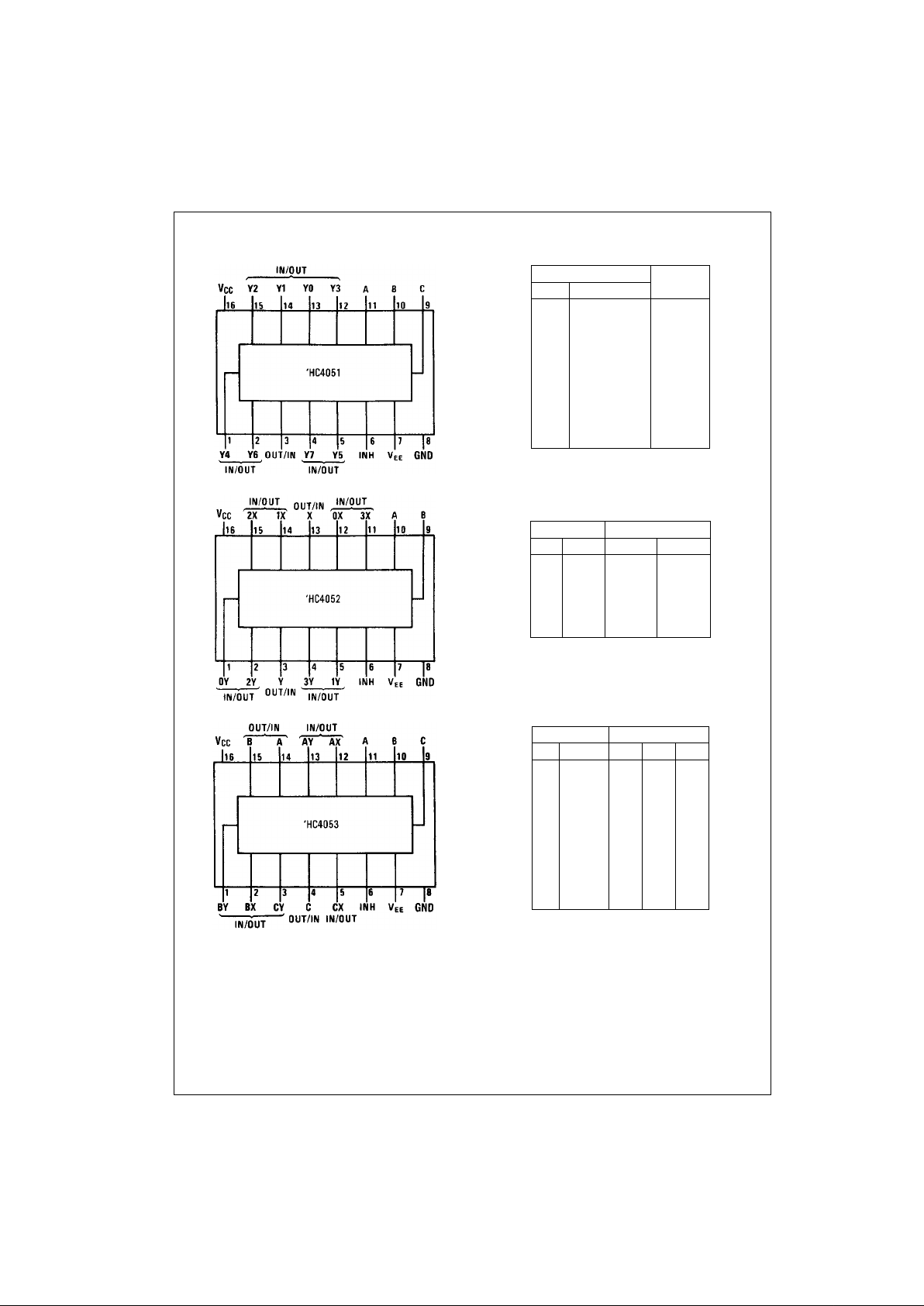
MM74HC4051: This de vice connects to gether the outp uts
of 8 switches, thus achieving an 8 channel Multiplexer. The
binary code placed on the A, B , and C select lines dete rmines which one o f the eight switches is “on”, and connects one of the eight inputs to the common output.
MM74HC4052: This d evice connects toge ther the output s
of 4 switches in two sets, thus achieving a pair of 4-channel
multiplexers. The binary code placed on the A, and B
select lines determine which switch in each 4 channel section is “on”, connecting one of the fo ur inputs in each section to its common output. This enables the implementation
of a 4-channel differential multiplexer.
MM74HC4053: This device contains 6 switches whose outputs are connected t ogether in pairs, thus implementing a
triple 2 channel multi plexer, or the equivalent of 3 singl epole-double throw con figurations. Each of the A, B, or C
select lines independently controls one pair of switches,
selecting one of the two switches to be “on”.
Features
■ Wide analog input voltage range: ±6V
■ Low “on” resistance:
50 typ. (V
CC–VEE
= 4.5V)
30 typ. (V
CC–VEE
= 9V)
■ Logic level translat ion to enable 5V logic w ith ±5V ana-
log signals
■ Low quiescent current: 80 µA maximum (74HC)
■ Matched Switch characteristic
Ordering Code:
Devices also availab le in Tape and Reel. Specify by appending th e s uffix let t er “X” to the ordering cod e.
Order Number Package Number Package Description
MM74HC4051M M16A 16-Lead Small Outline Integrated Circuit (SOIC), JEDEC MS-012, 0.150” Narrow
MM74HC4051WM M16B 16-Lead Small Outline Integrated Circuit (SOIC), JEDEC MS-013, 0.300” Wide
MM74HC4051SJ M16D 16-Lead Small Outline Package (SOP), EIAJ TYPE II, 5.3mm Wide
MM74HC4051MTC MTC16 16-Lead Thin Shrink Small Outline Package (TSSOP), JEDEC MO-153, 4.4mm Wide
MM74HC4051N N16E 16-Lead Plastic Dual-In-Line Package (PDIP), JEDEC MS-0010.300” Wide
MM74HC4052M M16A 16-Lead Small Outline Integrated Circuit (SOIC), JEDEC MS-012, 0.150” Narrow
MM74HC4052WM M16B 16-Lead Small Outline Integrated Circuit (SOIC), JEDEC MS-013, 0.300” Wide
MM74HC4052SJ M16D 16-Lead Small Outline Package (SOP), EIAJ TYPE II, 5.3mm Wide
MM74HC4052MTC MTC16 16-Lead Thin Shrink Small Outline Package (TSSOP), JEDEC MO-153, 4.4mm Wide
MM74HC4052N N16E 16-Lead Plastic Dual-In-Line Package (PDIP), JEDEC MS-0010.300” Wide
MM74HC4053M M16A 16-Lead Small Outline Integrated Circuit (SOIC), JEDEC MS-012, 0.150” Narrow
MM74HC4053WM M16B 16-Lead Small Outline Integrated Circuit (SOIC), JEDEC MS-013, 0.300” Wide
MM74HC4053SJ M16D 16-Lead Small Outline Package (SOP), EIAJ TYPE II, 5.3mm Wide
MM74HC4053MTC MTC16 16-Lead Thin Shrink Small Outline Package (TSSOP), JEDEC MO-153, 4.4mm Wide
MM74HC4053N N16E 16-Lead Plastic Dual-In-Line Package (PDIP), JEDEC MS-0010.300” Wide
www.fairchildsemi.com 2
MM74HC4051 • MM74HC4052 • MM74HC4053
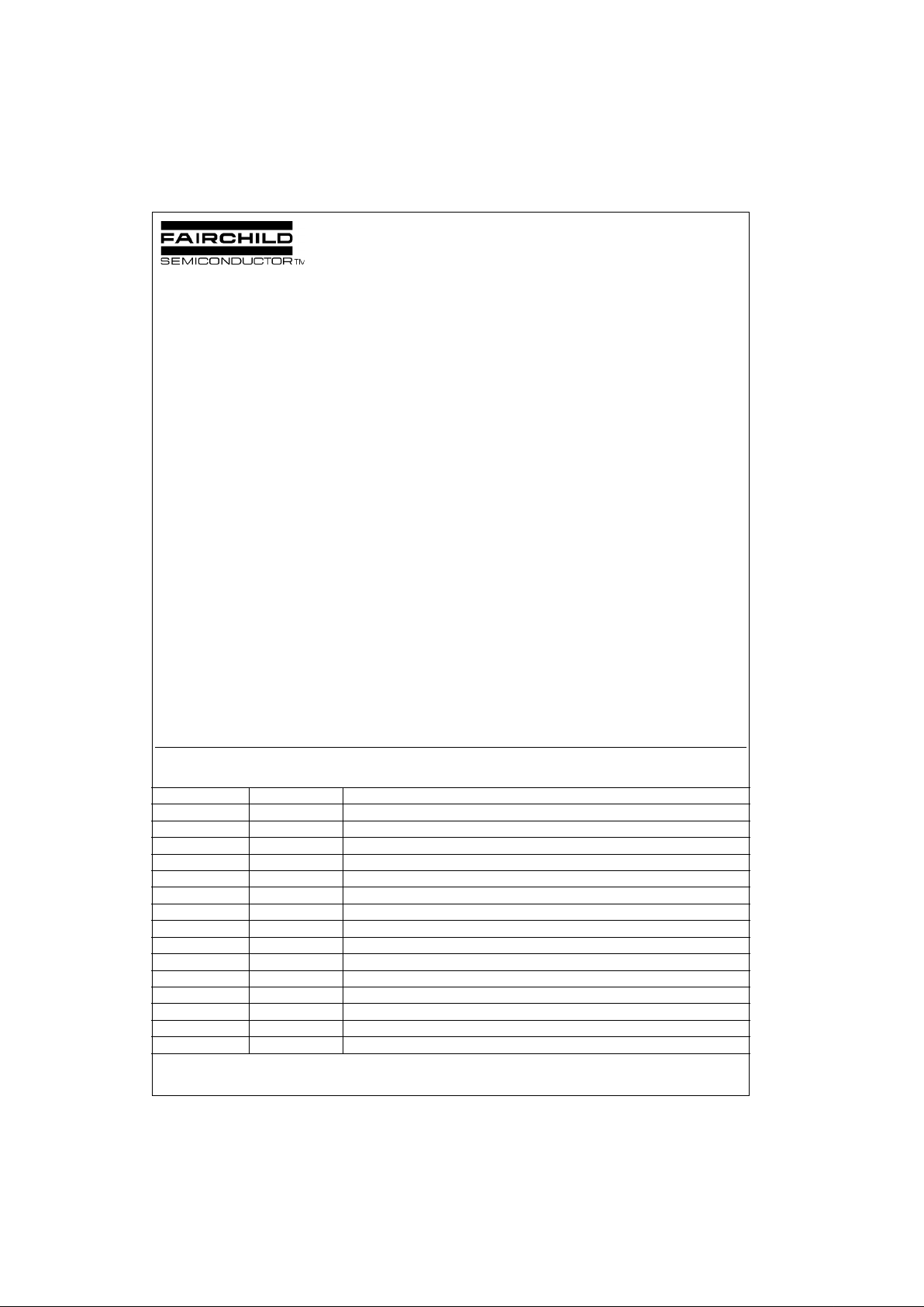
Connection Diagrams
Pin Assignments for DIP, SOIC, SOP and TSSOP
Top View
Top View
Top View
Tr uth Tables
MM744051
MM744052
MM744053
Input “ON”
InhCBAChannel
H XXX None
L LLL Y0
LLLH Y1
LLHL Y2
LLHH Y3
LHLL Y4
LHLH Y5
LHHL Y6
L HHH Y7
Inputs “ON” Channels
Inh B A X Y
H X X None None
LLL 0X 0Y
LLH 1X 1Y
LHL 2X 2Y
LHH 3X 3Y
Input “ON” Channels
InhCBA C b a
H X X X Non e None None
L L L L CX BX AX
LLLHCX BX AY
L L H L CX BY AX
LLHHCX BY AY
L H L L CY BX AX
LHLHCY BX AY
L H H L CY BY AX
L HHH CY BY AY
3 www.fairchildsemi.com
MM74HC4051 • MM74HC4052 • MM74HC4053
Logic Diagrams
MM74HC4051
MM74HC4052
MM74HC4053
www.fairchildsemi.com 4
MM74HC4051 • MM74HC4052 • MM74HC4053
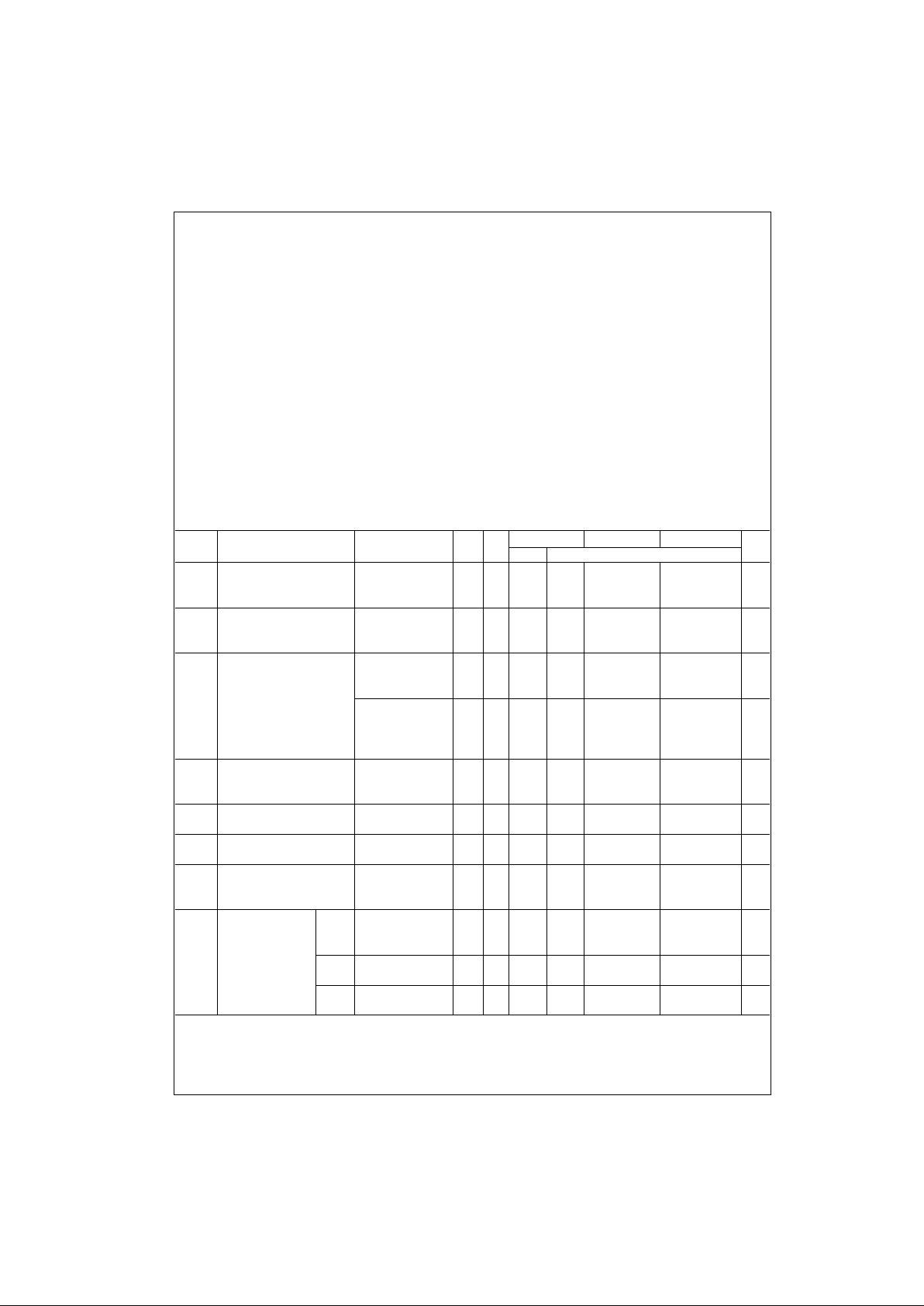
Absolute Maximum Ratings(Note 1)
(Note 2)
Recommended Operating
Conditions
Note 1: Absolute Maximum Ratings are those values beyond which dam-
age to the device may occur.
Note 2: Unless otherwise specified all voltages are referenced to ground.
Note 3: Power Dissipation temper ature dera ting — plas tic “N” packa ge: −
12 mW/°C from 65 °C to 85°C.
DC Electrical Characteristics (Note 4)
Supply Voltage (V
CC
) −0.5 to +7.5V
Supply Voltage (V
EE
) +0.5 to −7.5V
Control Input Voltage (V
IN
) −1.5 to V
CC
+1.5V
Switch I/O Voltage (V
IO
)V
EE
−0.5 to V
CC
+0.5V
Clamp Diode Current (I
IK
, IOK) ±20 mA
Output Current, per pin (I
OUT
) ±25 mA
V
CC
or GND Current, per pin (ICC) ±50 mA
Storage Temperature Range (T
STG
) −65°C to +150°C
Power Dissipation (P
D
)
(Note 3) 600 mW
S.O. Package only 500 mW
Lead Temperature (T
L
)
(Soldering 10 seconds) 260°C
Min Max Units
Supply Voltage (V
CC
)26V
Supply Voltage (V
EE
)0−6V
DC Input or Output Voltage
(V
IN
, V
OUT
)0V
CC
V
Operating Temperature Range (T
A
) −40 +85 °C
Input Rise or Fall Times
(t
r
, tf) VCC = 2.0V 1000 ns
V
CC
= 4.5V 500 ns
V
CC
= 6.0V 400 ns
Symbol Parameter Conditions
VEEV
CC
TA = 25°CTA = −40 to 85°CTA = −55 to 125°C
Units
Typ Guaranteed Limits
V
IH
Minimum HIGH Level 2.0V 1.5 1.5 1.5 V
Input Voltage 4.5V 3.15 3.15 3.15 V
6.0V 4.2 4.2 4.2 V
V
IL
Maximum LOW Level 2.0V 0.5 0.5 0.5 V
Input Voltage 4.5V 1.35 1.35 1.35 V
6.0V 1.8 1.8 1.8 V
R
ON
Maximum “ON” Resistance V
INH
= VIL, IS = 2.0 mA GND 4.5V 40 160 200 240 Ω
(Note 5) V
IS
= VCC to V
EE
−4.5V 4.5V 30 120 150 170 Ω
(Figure 1) −6.0V 6.0V 20 100 125 140 Ω
V
INH
= VIL, IS = 2.0 mA GND 2.0V 100 230 280 320 Ω
V
IS
= VCC or V
EE
GND 4.5V 40 110 140 170 Ω
(Figure 1) −4.5V 4.5V 20 90 120 140 Ω
−6.0V 6.0V 15 80 100 115 Ω
R
ON
Maximum “ON” Resistance V
CTL
= V
IL
GND 4.5V 10 20 25 25 Ω
Matching V
IS
= VCC to GND −4.5V 4.5V 5 10 15 15 Ω
−6.0V 6.0V 5 10 12 15 Ω
I
IN
Maximum Control V
IN
= VCCor GND ±0.1 ±1.0 ±1.0 µA
Input Current V
CC
= 2−6V
I
CC
Maximum Quiescent V
IN
= VCC or GND GND 6.0V 8 80 160 µA
Supply Current I
OUT
= 0 µA −6.0V 6.0V 16 160 320 µA
I
IZ
Maximum Switch “OFF” V
OS
= VCCor V
EE
GND 6.0V ±60 ±600 ±600 nA
Leakage Current V
IS
= VEEor V
CC
−6.0V 6.0V ±100 ±1000 ±1000 nA
(Switch Input) V
INH
= VIH (Figure 2)
I
IZ
Maximum Switch V
IS
= VCC to V
EE
GND 6.0V ±0.2 ±2.0 ±2.0 µA
“ON” Leakage HC4051 V
INH
= V
IL
−6.0V 6.0V ±0.4 ±4.0 ±4.0 µA
Current (Figure 3)
V
IS
= VCC to V
EE
GND 6.0V ±0.1 ±1.0 ±1.0 µA
HC4052 V
INH
= V
IL
(Figure 3) −6.0V 6.0V ±0.2 ±2.0 ±2.0 µA
V
IS
= VCC to V
EE
GND 6.0V ±0.1 ±1.0 ±1.0 µA
HC4053 V
INH
= VIL (Figure 3) −6.0V 6.0V ±0.1 ±1.0 ±1.0 µA
 Loading...