


MM74HCT273SJ
Fairchild Semiconductor MM74HCT273SJ, MM74HCT273SJX, MM74HCT273WM, MM74HCT273WMX, MM74HCT273MTC Datasheet
...
February 1984
Revised February 1999
MM74HCT273 Octal D-Type Flip-Flop with Clear
© 1999 Fairchild Semiconductor Corporation DS005760.prf www.fairchildsemi.com
MM74HCT273
Octal D-Type Flip-Flop with Clear
General Description
The MM74HCT273 utilizes advanced silicon-gate CMOS
technology. It has an input threshold and output drive sim ilar to LS-TTL with the low standby power of CMOS.
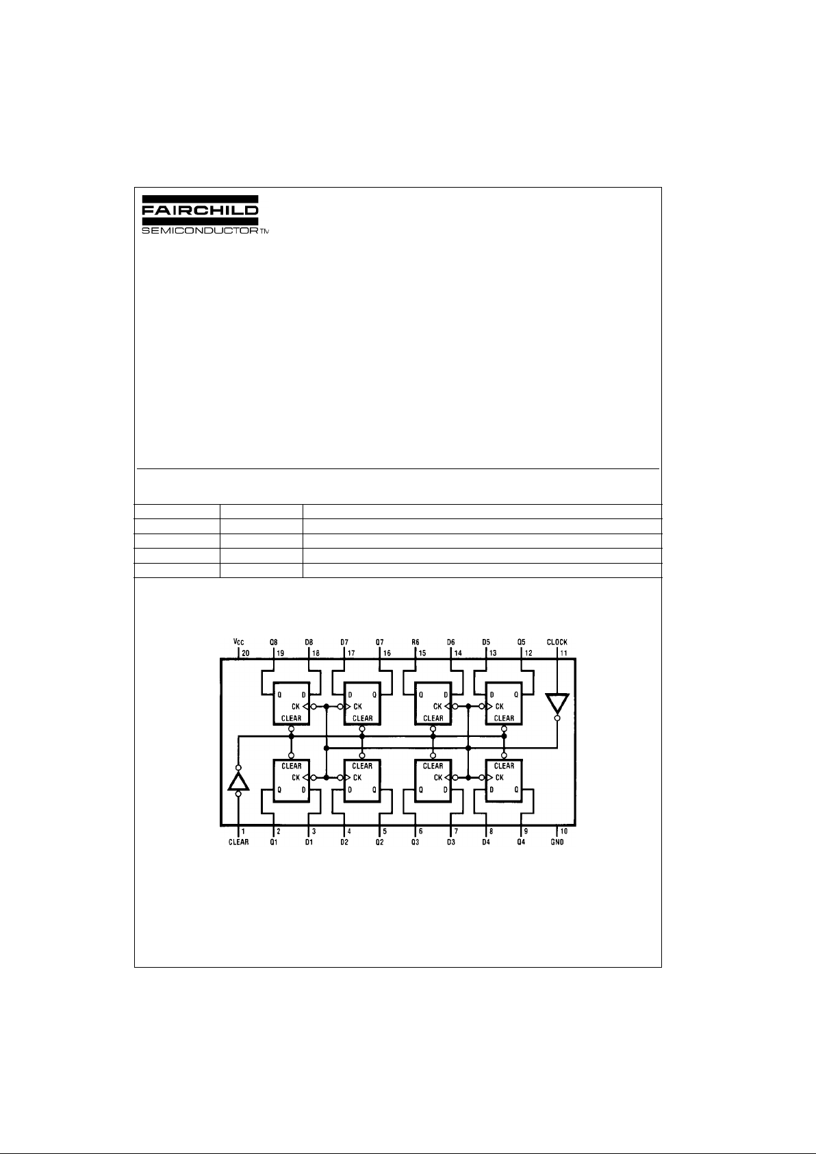
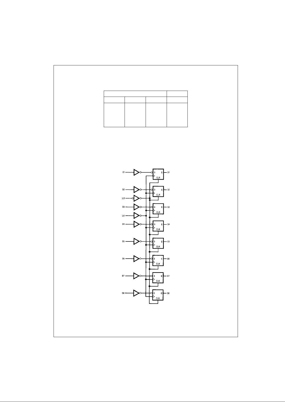
These positive edge-triggered flip-flops have a common
clock and clear-independe nt Q outp uts. Data o n a D inp ut,
having the specified set-up an d hold time, is t ransferred to
the corresponding Q o utp ut on t he posi t ive-going transition
of the clock pulse. The asynchronous cle ar forces all outputs LOW when it is LOW.
All inputs to this device are protected from damage due to
electrostatic discharge by diodes to V
CC
and ground.
MM74HCT devices are intended to interface TTL and
NMOS components to CMOS components. These parts
can be used as plug-in replacements to reduce system
power consumption in existing designs.
Features
■ Typical propagation delay: 20 ns
■ Low quiescent current: 80 µA maximum (74HCT series)
■ Fanout of 10 LS-TTL loads
Ordering Code:
Devices also available in Tape and Reel. Specify by appending the suffix letter “X” to the ordering code.
Connection Diagram
Pin Assignments for DIP, SOIC, SOP and TSSOP
Top View
Order Number Package Number Package Description
MM74HCT273WM M20B 20-Lead Small Outline Integrated Circuit (SOIC), JEDEC MS-013, 0.300” Wide
MM74HCT273SJ M20D 20-Lead Small Outline Package (SOP), EIAJ TYPE II, 5.3mm Wide
MM74HCT273MTC MTC20 20-Lead Thin Shrink Small Ou tline Package (TSSOP), JEDEC MO-153, 4.4mm Wide
MM74HCT273N N20A 20-Lead Plastic Dual-In-Line Packag e (PDIP), JEDEC MS-001, 0.300” Wide
www.fairchildsemi.com 2
MM74HCT273
Truth Table
(Each Flip-Flop)
H = HIGH Level (steady-state)
L = LOW Level (steady-state)
X = Don’t Care
↑ = Transition from LOW-to-HIGH level
Q0 = The level of Q before the indicated stead y -s ta t e input
conditions were established.
Logic Diagram
Inputs Outputs
Clear Clock D Q
LXXL
H ↑ HH
H ↑ LL
HLXQ0
3 www.fairchildsemi.com
MM74HCT273
Absolute Maximum Ratings(Note 1)
(Note 2)
Recommended Operating
Conditions
Note 1: Absolute Maximum Rati ngs are tho se values b eyond which d am-
age to the device may occur.
Note 2: Unless otherwise specified all voltages are referenced to ground.
Note 3: Power dissipation temperature de rating—p lastic “N ” package : −12
mW/°C from 65°C to 85°C.
DC Electrical Characteristics
VCC = 5V ± 10% unless otherwise specified
Note 4: Measured pe r pin, all other inputs held at VCC or GND.
Supply Voltage (VCC) −0.5V to + 7.0V
DC Input Voltage (V
IN
) −1.5V to VCC + 1.5V
DC Output Voltage (V
OUT
) −0.5V to VCC + 0.5V
Clamp Diode Current (I
IK
, IOK) ±20 mA
DC Output Current, per Pin (I
OUT
) ±25 mA
DC V
CC
or GND Current, per Pin (ICC) ±50 mA
Storage Temperature Range (T
STG
) −65°C to + 150°C
Power Dissipati on (P
D
)
(Note 3) 600 mW
S.O. Package only 500 mW
Lead Temperature (T
L
)
(Soldering, 10 seconds) 260°C
Min Max Units
Supply Voltage (V
CC
)4.55.5V
DC Input or Output Voltage
(V
IN
, V
OUT
)0V
CC
V
Operating Temperature Range (T
A
) −40 +85 °C
Input Rise or Fall Times
(t
r
, tf) 500 ns
Symbol Parameter Conditions
TA = 25°CTA = −40°C to 85°CTA = −55°C to 125°C
Units
Typ Guaranteed Limits
V
IH
Minimum HIGH Level 2.0 2.0 2.0 V
Input Voltage
V
IL
Maximum LOW Level 0.8 0.8 0.8 V
Input Voltage
V
OH
Minimum HIGH Level VIN = VIH or V
IL
Output Voltage |I
OUT
| = 20 µAV
CCVCC
−0.1 VCC−0.1 VCC−0.1 V
|I
OUT
| = 4.0 mA, VCC = 4.5V 4.2 3.98 3.84 3.7 V
|I
OUT
| = 4.8 mA, VCC = 5.5V 5.2 4.98 4.84 4.7 V
V
OL
Minimum LOW Leve l VIN = VIH or V
IL
Voltage |I
OUT
| = 20 µA 0 0.1 0.1 0.1 V
|I
OUT
| = 4.0 mA, VCC = 4.5V 0.2 0.26 0.33 0.4 V
|I
OUT
| = 4.8 mA, VCC = 5.5V 0.2 0.26 0.33 0.4 V
I
IN
Maximum Input VIN = VCC or GND, ±0.1 ±1.0 ±1.0 µA
Current VIH or V
IL
I
CC
Maximum Quiescent VIN = VCC or GND 8 80 160 µA
Supply Current I
OUT
= 0 µA
VIN = 2.4V or 0.5V (Note 4) 0.6 0.8 0.9 mA
 Loading...